Electric field driven magnetic domain wall motion in ferromagnetic-ferroelectric heterostructures
Abstract
We investigate magnetic domain wall (MDW) dynamics induced by applied electric fields in ferromagnetic-ferroelectric thin-film heterostructures. In contrast to conventional driving mechanisms where MDW motion is induced directly by magnetic fields or electric currents, MDW motion arises here as a result of strong pinning of MDWs onto ferroelectric domain walls (FDWs) via local strain coupling. By performing extensive micromagnetic simulations, we find several dynamical regimes, including instabilities such as spin wave emission and complex transformations of the MDW structure. In all cases, the time-averaged MDW velocity equals that of the FDW, indicating the absence of Walker breakdown.
pacs:
75.78.Fg, 75.30.Gw, 75.78.CdMagnetic domain wall (MDW) dynamics in nanoscale ferromagnetic wires and strips, as well as in thin films, is a subject of major technological importance for the operation of potential future magnetic memory PAR-08 and logic devices ALL-05 ; JAW-09 . While current efforts to construct such devices mostly focus on spin-polarized electric currents BER-96 ; SLO-96 or applied magnetic fields SHI-11 as the driving force, a promising low-power alternative has been demonstrated in recent experiments LAH-12 where electric fields move the MDWs in ferromagnetic-ferroelectric heterostructures. In such configurations, the MDWs in the ferromagnetic layer are strongly pinned onto ferroelectric domain walls (FDWs) in the ferroelectric sublayer via elastic interactions. Consequently, when an applied electric field displaces the FDWs, the MDWs are dragged along.
From a fundamental physics point of view, the question of the nature of this driving protocol is very important. Indeed, the electric field driving mechanism of MDWs differs substantially from the more conventional driving modes where either a magnetic field or spin-polarized electric current are used to move MDWs. While the effect of an applied electric field on magnetic field SCH-12 ; CHI-12 ; BAU-13 and spin-polarized current LEI-13 driven MDW motion has been considered, the nature of fully electric field driven MDW dynamics in ferromagnetic-ferroelectric heterostructures remains elusive.
In this Letter, we present a detailed numerical study of electric field driven MDW dynamics, including the short time scale details which have so far not been accessible experimentally. We consider two different 90∘ MDWs, one being magnetostatically charged and the other uncharged. Our results highlight the different nature of the electric field driving mechanism as compared to well-known magnetic field and electric current driven MDW motion: For all applied FDW velocities, the MDW moves along with a time-averaged velocity equal to the FDW velocity. Thus, the sharp decrease of the average velocity associated with Walker breakdown SHI-11 ; SCH-74 ; NAK-03 ; BEA-05 ; HAY-07 in magnetic field and electric current driven MDW dynamics is absent. For small FDW velocities, the MDW coupled to it is found to follow the moving FDW nearly quasistatically, without significant changes in the internal MDW structure. Above a threshold velocity, this close-to-quasistatic behavior breaks down, with various instabilities occurring depending on the MDW type (charged or uncharged) and the material parameters. For uncharged MDWs these instabilities comprise oscillatory MDW motions or complicated transformations of the MDW structure, while the emission of regular spin waves is observed for charged MDWs.
In ferromagnetic-ferroelectric thin-film heterostructures, the anisotropy of the ferromagnetic layer is laterally modulated via local strain transfer from ferroelectric domains and inverse magnetostriction. If polarization rotation between ferroelectric domains is less than 180∘ (i.e. if the domain pattern consists of FDWs that are both ferroelectric ferroelastic), minimization of the anisotropy energy can lead to full imprinting of ferroelectric domains into the ferromagnetic layer LAH-11-1 ; LAH-11-2 ; CHO-12 ; LAH-12-2 . Importantly, abrupt rotation of the ferroelectric polarization at FDWs and the concurrent instant change of magnetic anisotropy in the adjacent ferromagnet strongly pins the MDWs onto their ferroelectric counterparts. The reverse effect, i.e. modulation of the ferroelectric properties due to magnetization reversal in the ferromagnetic film, does not occur due to a pronounced asymmetry in the strain coupling mechanism. The maximum strain that can be transferred from a ferroelectric domain is given by the elongation of the structural unit cell. For archetypical tetragonal BaTiO3 at room temperature, this is 1.1%. Strain transfer from a ferromagnetic material to a ferroelectric layer via magnetostriction, on the other hand, is typically several orders of magnitude smaller HAN-00 . As a result, ferromagnetic effects on the dynamics of the ferroelectric sub-system can be safely neglected, and electric field induced MDW propagation is accurately modeled using a moving magnetic anisotropy boundary (AB) in the ferromagnetic layer.
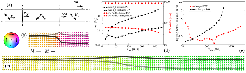
In our micromagnetic simulations, an AB separating two regions of uniform uniaxial anisotropies is moved with constant velocity (Fig. 1(a)), corresponding to the propagation velocity of the underlying FDW. The angle between the magnetic anisotropy axes is 90∘, which in practice can be obtained by strain coupling to in-plane domains of BaTiO3 LAH-11-1 ; LAH-11-2 . In an experiment, would be controlled by the magnitude of an applied electric field LIT-55 ; JO-09 ; SON-13 . Coarse-grained Monte Carlo simulations indicate that ferroelectric DW speeds of up to several km/s are possible SHI-07 . Our simulations are performed with the GPU-based micromagnetic simulator MuMax VAN-11 . To study the time evolution of the magnetization , we solve the Landau-Lifshitz (LL) equation,
where is the effective magnetic field (with contributions from the exchange, anisotropy and demagnetizing fields), and is the gyromagnetic ratio. The reference sample in this study is a 15 nm thick Co60Fe40 layer on top of a BaTiO3 substrate, corresponding to the experimental system in LAH-11-1 , with saturation magnetization =1.7 A/m, uniaxial magnetic anisotropy strength =1.7 J/m3, exchange constant =2.1 J/m, and damping constant =0.015. All material parameters are varied around these values to investigate their effect on the observed MDW dynamics. By considering periodic boundary conditions in both - and -direction, we mimic MDW propagation in an infinite film. The simulation window is restricted to two 6.4 wide domains with orthogonal anisotropy axes over a length of 200 nm, see Fig. 1(a). The resulting 90∘ MDWs can be of two different types, magnetostatically charged or uncharged, depending on the magnetization directions in the domains FRA-12 . The widths of these two MDW types differ substantially as illustrated by their micromagnetic structures in Figs. 1(b) and (c). We consider both cases separately and show that their dynamic behavior is very different.
For small imposed , both the charged and uncharged MDW follow the motion of the AB. While the magnetization of the uncharged DW is completely in-plane at rest, an out-of-plane magnetization component develops and the DW width reduces with increasing (Fig. 1(d)). These deformations are similar to those observed during magnetic field and current driven MDW motion in magnetic nanowires and strips, where the appearance of an out-of-plane magnetization component and a narrowing of the MDW are precursors of Walker breakdown SHI-11 ; SCH-74 ; NAK-03 ; BEA-05 ; HAY-07 . In addition, the uncharged MDW lags slightly behind the AB by a distance that increases with (Fig. 1(e)). For higher AB speeds, a breakdown of quasistatic MDW motion occurs at a threshold velocity . In comparison, the internal structure of the charged MDW is much more robust against dynamic deformations, as illustrated by the negligible out-of-plane magnetization and nearly constant MDW width in Fig. 1(d).
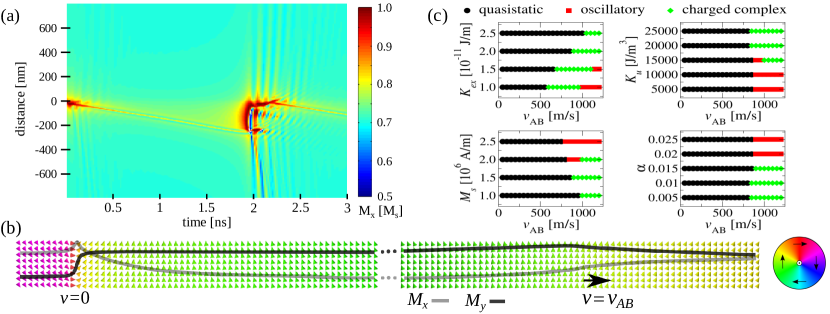
The dynamics of the uncharged MDW above the threshold velocity depends on the material parameters. Two possible scenarios are observed in our simulations. In the first, termed here as “oscillatory”, the MDW first lags increasingly behind the AB until a maximum distance is reached (about 200 nm for the reference parameters). At that point, the MDW is abruptly pulled back to the AB (a process that also involves the emission of spin waves), after which the MDW starts to lag behind the AB again (Fig. 2(a)). This cycle of events is repeated continuously. The second scenario, labeled as “charged complex”, is significantly different. In this case, the initially uncharged MDW transforms by creating two oppositely charged MDWs. After this, one of the charged MDWs follows the AB, while a MDW complex comprising the original uncharged MDW and the other charged MDW is left behind. The MDW complex subsequently slows down and eventually stops moving since it is no longer pinned onto a moving FDW (the AB in our simulations). This behavior is somewhat analogous to recent observations of a break-up of the compact domain wall structure in wide submicrometer wires ZIN-11 . An example of the resulting configuration is shown in Fig. 2(b). This process obeys the principle of charge conservation, i.e. the net charge of the newly created charged MDWs is zero. Although the deformations of an uncharged MDW below are reminiscent of Walker breakdown, the physical consequences above are different compared to magnetic field or current driven magnetic systems. In the latter cases, an abrupt decrease in the time-averaged MDW speed is often observed beyond breakdown due to magnetization precession within the MDW. The average speed of an initially uncharged MDW that is strongly coupled to a FDW equals the FDW velocity, and it moves either in an “oscillatory” fashion or as a charged MDW after the transformation.
The dependence of the threshold velocity and the type of dynamic behavior on the micromagnetic parameters are illustrated by the phase diagrams of Fig. 2(c). The maximum distance between a moving uncharged MDW and the AB in the small imposed regime (Fig. 1(e)), i.e. the “stiffness” of the pinning potential that is created by the AB, determines the dynamics above : Material parameters that give rise to a large lagging behind distance in the low velocity regime lead to “oscillatory” behavior above , while small MDW-AB distances below imply a “charged complex” scenario for (Fig 2(c)). The threshold velocity strongly depends on the exchange constant, with weaker exchange interactions resulting in smaller . Thus, in order to experimentally observe non-trivial high velocity dynamic effects in ferromagnetic-ferroelectric heterostructures, it would be favorable to use magnetic materials that combine a small exchange constant and large magnetostriction, with the latter needed in order to have a sufficiently strong pinning of the MDWs onto their ferroelectric counterparts.
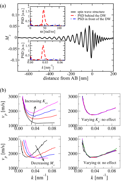
The dynamic behavior of charged MDWs is different from that of uncharged MDWs at high AB velocities. The much larger width of the charged MDW implies that it can move fast without encountering major instabilities. This is due to the much lower rate of spin rotation needed to move the wide charged MDW, as compared to the narrow uncharged MDW. The charged MDW starts to emit spin waves when exceeds the minimum spin wave phase velocity. A typical wave profile of a charged MDW at = 1800 m/s is shown in Fig. 3(a). The spin waves that are emitted have a phase velocity which equals , but their well-defined wave number , and thus their frequency, is different in front and behind the moving MDW (insets of Fig. 3(a)). This behavior is similar to recent numerical observations of fast MDW dynamics in magnetic nanotubes YAN-11 .
The emitted spin waves in front and behind the MDW are characterized by dispersion graphs ( versus ), which we obtained by considering different AB velocities. The dependence on material parameters (same values as in Fig. 2(c)) is summarized in Fig. 3(b). The threshold velocity for spin wave emission corresponds to the minimum spin wave phase velocity . At this velocity, the spin waves moving in front and behind the MDW have the same wave number and frequency. From Fig. 3(b) it is clear that the exchange constant has a large influence on . The saturation magnetization does barely influence , but it influences the corresponding wave number. The dispersion properties of the spin waves emitted in front of the MDW are much more affected than those behind the MDW when and are varied. The strength of the uniaxial magnetic anisotropy and the magnetic damping constant have no effect on the emission spectra. The independence of is caused by the cancellation of two opposing effects, one related to the emission of spin waves (a stronger AB pumps more energy into the spin waves) and another due to the stiffness of the medium in which the spin waves propagate (larger anisotropy implies a stiffer medium). The negligible influence of on the dispersion properties of spin waves is well known and often utilized in micromagnetic studies.
To summarize, we have studied electric field induced MDW motion in ferromagnetic-ferroelectric heterostructures. The driving force, which can be modeled as an anisotropy boundary moving in the ferromagnetic layer, provides a mechanism for MDW dynamics exhibiting properties that are fundamentally different from magnetic field and electric current driven MDW motion. Depending on the MDW type and material parameters, spin wave emission and MDW transformations are found for high driving velocities. Due to the robustness of this driving mechanism, manifested by the absence of the Walker breakdown, electric field driven MDW motion could open up exciting opportunities in the design of low power spintronics applications such as magnetic memory and logic devices.
Acknowledgments. We thank Mikko Alava for a critical reading of the manuscript. This work has been supported by the Flanders Research Foundation (B.V.d.W.), the Academy of Finland through a Postdoctoral Researcher’s Project (L.L., project no. 139132), an Academy Research Fellowship (L.L., project no. 268302), an Academy project (S.v.D., project no. 260361) and via the Centres of Excellence Program (L.L., project no. 251748), as well as by the Theory Programme of Helsinki Insitute of Physics (L.L.), by the Finnish Doctoral Program in Computational Sciences (K.J.A.F.) and by the European Research Council (S.v.D., ERC-2012-StG 307502-E-CONTROL)
References
- (1) S. S. P. Parkin, M. Hayashi, and L. Thomas, Science 320, 190 (2008).
- (2) D. A. Allwood, G. Xiong, C. C. Faulkner, D. Atkinson, D. Petit, and R. P. Cowburn, Science 309, 1688 (2005).
- (3) J. Jaworowicz, N. Vernier, J. Ferré, A. Maziewski, D. Stanescu, D. Ravelosona, A. S. Jacqueline, C. Chappert, B. Rodmacq, and B Diény, Nanotechnology 20, 215401 (2009).
- (4) L. Berger, Phys. Rev. B. 54, 9353 (1996).
- (5) J. C. Slonczewski, J. Magn. Magn. Mater. 159, L1 (1996).
- (6) J. Shibata, G. Tatara, and H. Kohno, J. Phys. D: Appl. Phys. 44, 384004 (2011).
- (7) T. H. E. Lahtinen, K. J. A. Franke, and S. van Dijken, Sci. Rep. 2, 258 (2012).
- (8) A. J. Schellekens, A. van den Brink, J. H. Franken, H. J. M. Swagten, and B. Koopmans, Nat. Commun. 3, 847 (2012).
- (9) D. Chiba, M. Kawaguchi, S. Fukami, N. Ishiwata, K. Shimamura, K. Kobayashi, and T. Ono, Nat. Commun. 3, 888 (2012).
- (10) U. Bauer, S. Emori, and G. S. D. Beach, Nat. Nanotech. 8, 411 (2013).
- (11) N. Lei, T. Devolder, G. Agnus, P. Aubert, L. Daniel, J-V Kim, W. Zhao, T. Trypiniotis, R. P. Cowburn, C. Chappert, D. Ravelosona, and P. Lecoeur, Nat. Commun. 4, 1378 (2013).
- (12) N. L. Schryer and L. R. Walker, J. Appl. Phys. 45, 5406 (1974).
- (13) Y. Nakatani, A. Thiaville, and J. Miltat, Nat. Mater. 2, 521 (2003).
- (14) G. S. D. Beach, C. Nistor, C. Knutson, M. Tsoi, and J. L. Erskine, Nat. Mater. 4, 741 (2005).
- (15) M. Hayashi, L. Thomas, C. Rettner, R. Moriya, and S. S. P. Parkin, Nat. Phys. 3, 21 (2007).
- (16) T. H. E. Lahtinen, J. O. Tuomi, and S. van Dijken, Adv. Mater. 23, 3187 (2011).
- (17) T. H. E. Lahtinen, J. O. Tuomi, and S. van Dijken, IEEE Trans. Magn. 47, 3768 (2011).
- (18) R. V. Chopdekar, V. K. Malik, A. Fraile Rodríguez, L. Le Guyader, Y. Takamura, A. Scholl, D. Stender, C. W. Schneider, C. Bernhard, F. Nolting, and L. J. Heyderman, Phys. Rev. B 86, 014408 (2012).
- (19) T. H. E. Lahtinen, Y. Shirahata, L. Yao, K. J. A. Franke, G. Venkataiah, T. Taniyama, and S. van Dijken, Appl. Phys. Lett. 101, 262405 (2012).
- (20) R. C. O’Handley, Modern Magnetic Materials: Principles and Applications (John Wiley & Sons, Inc., New York, 2000).
- (21) E. A. Little, Phys. Rev. 98, 978 (1955).
- (22) J. Y. Jo, S. M. Yang, T. H. Kim, H. N. Lee, J.-G. Yoon, S. Park, Y. Jo, M. H. Jung, and T. W. Noh, Phys. Rev. Lett. 102 045701 (2009).
- (23) J. Y. Son and S. M. Yoon, Ceram. Int. 39, 4031 (2013).
- (24) Y.-H. Shin, I. Grinberg, I-W. Chen, and A. M. Rappe, Nature 449, 881 (2007).
- (25) A. Vansteenkiste and B. Van de Wiele, J. Magn. Magn. Mater. 323, 2585 (2011).
- (26) K. J. A. Franke, T. H. E. Lahtinen, and S. van Dijken, Phys. Rev. B 85, 094423 (2012).
- (27) The lagging behind distance in the quasistatic regime is determined by quadratic interpolation of the discretization points defining the center of the domain wall.
- (28) C. Zinoni, A. Vanhaverbeke, P. Eib, G. Salis, and R. Allenspach, Phys. Rev. Lett. 107, 207204 (2011).
- (29) M. Yan, C. Andreas, A. Kákay, F. Garcia-Sánchez, and R. Hertel, Appl. Phys. Lett. 99, 122505 (2011).