Electronic transport in BN-substituted bilayer graphene nano-junctions
Abstract
We investigated a suspended bilayer graphene where the bottom (top) layer is doped by boron (nitrogen) substitutional atoms by using Density Functional Theory (DFT) calculations. We found that at high dopant concentration (one B-N pair every 32 C atoms) the electronic structure of the bilayer does not depend on the B-N distance but on the relative occupation of the bilayer graphene sub-lattices by B and N. We found that a large built in electric field is established between layers, giving rise to an energy gap. We further investigated the transport properties and found that intra-layer electron current is weakly influenced by the presence of these dopants while the inter-layer current is significantly enhanced for biases allowing the energy alignment of N and B states. This effect leads to current rectification in asymmetric junctions.
Bilayer graphene (BLG) is a two-dimensional material constituted by two stacked graphene layers. BLG has recently attracted much interest because it show exceptionally high charge mobility like in single layer graphene. Charge transport in BLG is tied the in-plane direction of each of the two layers. As a consequence, BLG has been proposed to be more suitable than single layer graphene to realize carbon-based, field effect logic devices Fiori2009 ; Bane2009 ; li11 . However, due to the small density of states of BLG at the Fermi level, in order to apply a gate voltage across BLG, very large electric fields are needed. This has deleterious impact on the performance and stability of gated BLG. For instance, graphene and BLG deposited on oxide dielectric such as SiO2 show a large hysteresis in the I-V curve, due to the charging/discharging of point defects in the oxide. Moreover, charged impurities in the gate oxide and at the graphene-gate interface,have been shown to reduce dramatically the mobility of graphene-based devices lafkioti10 ; liao10 .
On the other hand, the low density of states can be exploited to induce a large built it electric field in BLG. In fact, even the addition or removal of a small amount of charge from each layer causes an abrupt change of the Fermi level. In this paper we simulate a suspended bilayer graphene nano-junctions where boron and nitrogen atoms substitute carbon atoms from the top and bottom layers, respectively. The equal number of B and N atoms assures that the system is neutral. By first principles calculations we have found that a large built in electric field is then established, which is the consequence of two effects: the first is the Fermi-level mismatch between the B-rich and N-rich layer, the second is a partial charge transfer between the two layers. As a consequence, a small energy gap appears enabling this system to be employed for nano-electronics applications. In view of this, we also investigated the ballistic transport in a nano-junction containing B and N substitutional atoms.
We performed DFT calculations with the local-basis SIESTA code SIESTA1999 ; 30Artacho ; 29Soler ; 28Ordejon . We used norm-conserving pseudopotentials 32Troullier and the DZP basis set. The exchange correlation potential is described by the PBE functional 26Perdew and the weak van der Waals forces between the graphene layers are described by a classical term, parametrized by Grimme Grimme2004 ; Grimme2006 . With this method, we obtained an interlayer distance of 3.32 Å for pristine BLG, in good agreement with the experimental value of 3.36 Å . In every subsequent calculation, we fixed the in-plane lattice constant to the calculated value is 2.474 Å, which is close to the experimental value of 2.46 Å . We employed the slab-dipole correction SIESTA1999 .
We simulated the doping of each layer by constructing a 44 supercell i.e. 32 carbon atoms per layer with a single B-N substitutional pair. The electronic properties of the system depends on the the relative position of the two dopants in the graphene sub-lattices. In fact, graphene is a bipartite lattice and the for BLG the two sub lattices are no more equivalent. The first sub-lattice (S1) is constituted by carbon atoms sitting on top of carbon atoms from the other layer. The second sub-lattice (S2) is constituted by carbon atoms positioned above the geometrical center of the hexagons from the other layers.
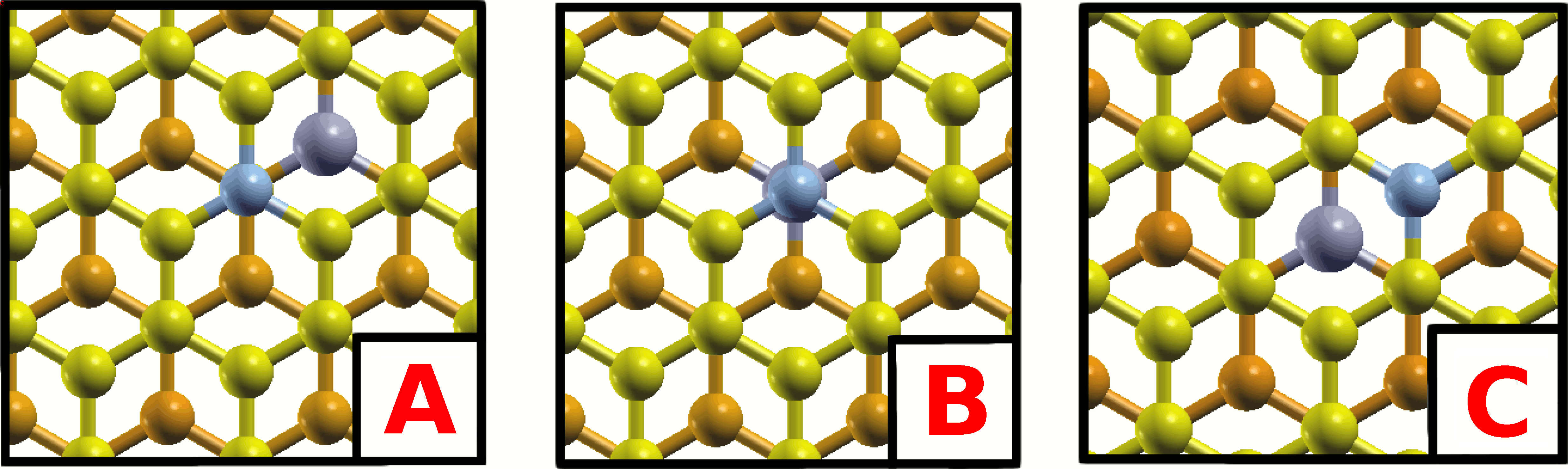
Thus, in BN-substituted BLG, with only one BN pair, only three configurations are permitted. The first is when B and N belong to different sub-lattices (A in Fig. 1); the second is characterized by B and N belonging to the first sub-lattice and are one on top of each other (B in Fig. 1). In the third configuration B and N occupy both the S2 sub-lattice (C in Fig. 1). In the 44 supercell, additional arrangements are possible which differ from A, B and C for the relative B-N distance. We verified that for a given BN-substitution of the two sublattices, the distance between the impurities has a minor influence the electronic properties of the system. This is reasonable because the added/removed electron in each graphene layer is almost completely delocalized in its own sub-lattice.
In the rest, we concentrate on the most energetically stable system, i.e. the configuration C. This configuration is 0.06 eV lower in energy than B and 0.07 eV than A. Configuration C is insulating, while A and A are metallic.
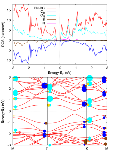
In Fig. 2 we report the density of states (DOS) and the band structure of this configuration. The system is an insulator, with an indirect Kohn-Sham band gap of 0.35 eV, between the high symmetry points K and M. Moreover, the characteristic “V-shaped” DOS of graphene centered around the Dirac point, is still visible in the plot, except that the two linear branches are separated away by an energy = 1.9 eV. The DOS of the system is similar to that of pristine BLG but with an external applied electric field of 0.37 V/Å along the direction perpendicular to the sheets.
To rationalize the energy separation between the Dirac, we performed additional calculations of the two isolated doped layers and of a pristine graphene layers, and of BLG in presence of perpendicular electric field. We have found that is given by the sum of two contributions: where the first term is the built in electric field generated by the Fermi-level mismatch, in absence of charge transfer (i.e. when the two layers are separated by a large distance) and the second term is due to charge transfer between the two layers. Thus, the first term represents a purely classical capacitor, whereas the second term is of purely quantum origin, and depends on the overlap of the wavefunctions belonging to the two different layers. A full account of the derivation of and is presented in the additional material.
From the band structure one can also note that the highest occupied band belongs to the B-doped layer while the lowest unoccupied belongs to the N-doped layer. The difference of the electronic structure between the two graphene layers with donor or acceptor dopants, motivated us to simulate the electronic ballistic transport through BN-doped BLG nano-junctions.
The first principles quantum transport calculations were performed using the TranSIESTA code 38Brandbyge , which employs the non-equilibrium Green’s function (NEGF) formalism in conjunction with DFT. Within the NEGF-DFT formalism, the system has been divided into three regions: the left and right electrodes, and the transition region. The transition part contains the portion of physical electrodes, the so-called right and left junction, where all screening effects take place. In order to apply an external bias, the Fermi level of the electrodes are shifted relative to each other and the electronic occupations of the system are determined by electrochemical potentials of electrodes.
We first consider the electron transport through a finite BN-doped region. The left and right electrodes are made of pristine BLG while the scattering region containing a single pair of BN-doping BLG, as shown in Fig. 3. The scattering region contains 64 atoms, while the electrodes are made of 32 atoms each.
Although we have found that the two dopants represent a weak perturbation to BLG, they can nevertheless play a role in transport, by reducing the number of available channels. The -resolved DOS of the system is shown in Fig. 4 together with those of prisitne BLG. The effect of doping is the appearance of new states: at about 2 eV at () the occupied B orbital, with a small dispersion on . The state about 1.5 eV is the N nitrogen orbital, showing a negligible dispersion along .
Additionally, four other states appear in the projected-DOS gap. Two states which are very close the band edges behave like Tamm-like states Tamm1932 emerging from the graphene bands. The one at negative energy has a large boron character and is localized on the B-doped graphene layer while that at positive energy is the N-doped layer counterpart. The remaining pair of states are Shockley-like states Shockley (1939) are are due to the discontinuity in the potential felt by the electron, in strict analogy with the classical surface states. Both these Tamn and Schockley are 1-D in character and are strongly localized. For this reason, they do not contribute to the electronic transport but they behave as a scattering centers.
We calculated the curve with the NEGF-DFT method, where the charge density is self-consistently updated upon the effect of the applied bias. Once the transmission probability is worked out, the current is obtained integrating in the energy window corresponding to the applied voltage.
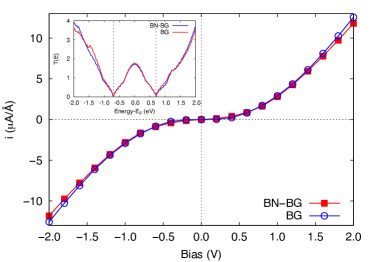
We show in Fig. 5 the curve for the doped BLG compared to the pristine BLG. The comparison shows that the I-V characteristics are very similar and that the current flowing in the BN-doped system is slightly smaller. Indeed the N and B states do not perturb the system in the energy range relevant for transport and the C network is preserved. Furthermore, the inter-layer current flow is much smaller than the intra-layer one. As an example, in the inset of Fig. 5 is reported the transmission probability for these two systems at an applied voltage of eV. They look very similar, especially in the bias energy window, further confirming our expectation.
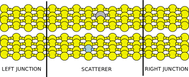
We now consider a “shingle” nano-junction, constituted by two semi infinite H-terminated graphene layers where the dopants are located in the contact region (Fig. 6). The electronic transport across this junction is a very interesting case, showing that when the carbon network is broken, for example when the graphene bilayer is formed by flakes overlapping to some extend, rectification can occur. In the present case, the electron current must flow from one layer to the other, overcoming an energy barrier this system breaks the left-right symmetry and behaves like a n-p nano-junction.
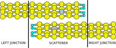
By comparing this nano-junction with the same system without BN-dopants, it is possible to study the effect of the single BN couple on the transport properties. As in the previous case the junction is completely contained in the scattering region, but the electrodes are now constituted by semi-infinite graphene layers.
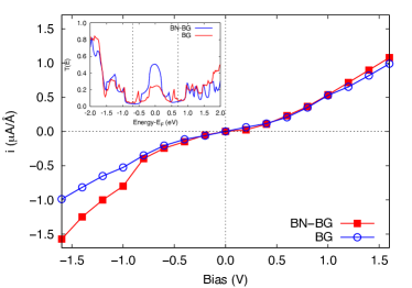
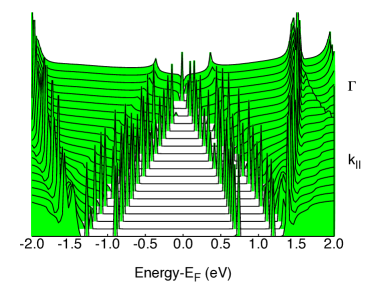
The computed I-V characteristic is reported in Fig. 7. The first finding is the reduction of the absolute value of the current by one order of magnitude. This reduction does not suppress completely the current flow because the partial overlap of the bands of graphene on different layers. We also note that for positive bias (i.e. for electrons which flow from the N-doped to the B-doped layer) the electron current through the doped junction is a bit larger then those obtained without the BN-pair. Therefore, the presence of these impurities play the role to lower the potential barrier between layers.
The most interesting results is the behavior of the junction at large negative biases: in this case the current of the doped system is significantly larger (of about 50%) than the pristine one. By inspecting the transmission functions (at 1.4 V bias, see the inset of Fig. 7), we found that this increase is not due to the entry of N or B related features in the energy window relevant for transport but instead to an increase of the tunnel probability in the middle of this range. A further analysis of the DOS confirms that this effect is due to the alignment of the N and B energy resonances, now shifted by the bias. In fact, for bias lower than 1.0 V, the filled B state and the empty N state start to align, allowing a preferential channel for interlayer current.
In conclusion, we studied the electronic and transport properties of a N and B doped graphene bilayer by first principles and we found that a strong electric field is established between the two layer because the opposite nature of the dopants (acceptor and donor), also creating a small energy gap. Our analysis showed a small effect of the dopants on the transport properties of the graphene bilayer. Differently, when the carbon network is broken like for overlapping graphene flakes, the interlayer current start to play the major role. In this case the presence of the dopants enhances the current but for negative biases only, originating a rectification effect in this n-p nano-junction.
References
- (1) M. Lafkioti, B. Krauss, T. Lohmann, U. Zschieschang, H. Klauk, K. v. Klitzing and J. H. Smet, Nano Lett. 10, 1149 (2010).
- (2) S.-L. Li, H. Miyazaki, H. Hiura, C. Liu K. Tsukagoshi, ACS Nano 5 (2011).
- (3) Z.-M. Liao, B.-H. Han, Y.-B. Zhou and D.-P. Yu, J. Chem. Phys. 133, 044703 (2010).
- (4) G. Fiori and G.Iannaccone, IEEE Electron Device Letters 30, 1096 (2009).
- (5) S. K. Banerjee, L.F. Register, E. Tutuc, D. Reddy, and A.H. MacDonald, IEEE Electron Device Letters 30, 158 (2009).
- (6) J. P. Perdew, K. Burke, and M. Ernzerhof, Phys. Rev. Lett. 77, 3865 (1996).
- (7) P. Ordejón, E. Artacho, and J.M. Soler, Phys. Rev. B 53, 441 (1996).
- (8) J. M. Soler, E. Artacho, J. D. Gale, A. García, J. Junquera, P. Ordejón, and D. V. Sánchez-Portal, J. Phys: Condens. Matter 14, 2745 (2002).
- (9) E. Artacho, E. Anglada, O. Dieguez, J. D. Gale, A. García, J. Junquera, R. M. Martin, P. Ordejón, J. M. Pruneda, D. V. Sánchez-Portal, and J. M. Soler, J. Phys: Condens. Matter 20 4208 (2008).
- (10) E. Artacho, D Sánchez-Portal, P. Ordejón, A. García, and J. M Soler, Phys. Stat. Sol. B 215, 809 (1999).
- (11) N. Troullier and J. L. Martins, Phys. Rev. B 43, 1993 (1991).
- (12) S. Grimme, J. Comput. Chem. 25, 1463 (2004).
- (13) S. Grimme, J. Comput. Chem. 27, 1787 (2006).
- (14) M. Brandbyge, J. L. Mozos, P. Ordejón, J. Taylor, and K. Stokbro, Phys. Rev. B 65, 5401 (2002).
- (15) I. Tamm, Phys. Z. Soviet Union 1, 733 (1932).
- Shockley (1939) W. Shockley, Phys. Rev. 56, 317 (1939).