Extrinsic spin Hall effects measured with lateral spin valve structures
Abstract
The spin Hall effect (SHE), induced by spin-orbit interaction in nonmagnetic materials, is one of the promising phenomena for conversion between charge and spin currents in spintronic devices. The spin Hall (SH) angle is the characteristic parameter of this conversion. We have performed experiments of the conversion from spin into charge currents by the SHE in lateral spin valve structures. We present experimental results on the extrinsic SHEs induced by doping nonmagnetic metals, Cu or Ag, with impurities having a large spin-orbit coupling, Bi or Pb, as well as results on the intrinsic SHE of Au. The SH angle induced by Bi in Cu or Ag is negative and particularly large for Bi in Cu, 10 times larger than the intrinsic SH angle in Au. We also observed a large SH angle for CuPb but the SHE signal disappeared in a few days. Such an aging effect could be related to a fast mobility of Pb in Cu and has not been observed in CuBi alloys.
pacs:
72.25.Ba, 72.25.Mk, 75.70.Cn, 75.75.-cI Introduction
The spin Hall effect (SHE) and its inverse (ISHE) are key ingredients for spintronic devices since they enable conversion of charge currents to and from spin currents without using ferromagnets and external magnetic fields maekawa_review_book . One of the typical examples of utilizing the ISHE is a detection of a spin dependent chemical potential arising from the spin Seebeck effect uchida_nature_2008 ; uchida_nat_mater_2010 ; uchida_nat_mater_2011 ; kirihara_nat_mater_2012 ; chien_prl_2013 ; saitoh_prl_2013 . The spin Seebeck effect converts heat into spin current, and the generated spin current can be electrically detected by the ISHEs of Pt uchida_nature_2008 ; uchida_nat_mater_2010 ; uchida_nat_mater_2011 ; kirihara_nat_mater_2012 and Au chien_prl_2013 ; saitoh_prl_2013 . Magnetization switching with a CoFeB/Ta bilayer film is another example of utilizing the SHE liu_science_2012 . A pure spin current, flow of only spin angular momentum without charge current, is generated by the SHE of Ta, and induces a spin transfer torque in the ferromagnetic layer. To realize the detection of the spin Seebeck effect as well as the magnetization switching, the ISHEs and SHEs of simple metals such as Pt uchida_nature_2008 ; uchida_nat_mater_2010 ; uchida_nat_mater_2011 ; kirihara_nat_mater_2012 ; liu_prl_2012 , Au chien_prl_2013 ; saitoh_prl_2013 , and Ta liu_science_2012 have been mainly used. Among them, Pt has been widely believed to be the best SHE material exhibiting a large spin Hall (SH) angle which represents the conversion yield between charge and spin currents. However it is a costly metal, unsuitable for the practical application. In addition, the SHEs of 4 and 5 transition metals originate from the intrinsic mechanism based on the degeneracy of orbits by spin-orbit (SO) coupling guo_prl_2008 ; tanaka_prb_2008 ; morota_prb_2011 . This fact indicates that it is difficult to modulate the SH angle artificially once the transition metal is fixed.
There is another type of SHE, the extrinsic SHE induced by scattering on impurities with strong SO interaction. There are two mechanisms in the extrinsic SHE, i.e., the skew scattering skew and the side jump side_jump . Unlike the case of the intrinsic SHE, the SH angle can be enhanced by changing the combination of host and impurity metals. According to recent theoretical calculations based on the skew scattering gradhand_prl_2010 ; gradhand_prb_2010 ; fert_prl_2011 , some combinations of noble metals and impurities can give rise to very large SH angles, for example in Cu or Ag doped with Bi. We have experimentally demonstrated the extrinsic SHEs induced by Ir niimi_prl_2011 and Bi niimi_prl_2012 impurities in Cu. As for Ir-doped Cu, the magnetization switching has already been realized using the SHE of CuIr alloys ohno_apl_2013 . Since Cu is a typical inexpensive metal, Cu-based alloys are desirable for future application of spintronic devices. In this paper, we studied the SHEs of CuBi, Au, AgBi, and CuPb using the spin absorption method in the lateral spin valve (LSV) structure. We have already reported that CuBi alloys show a very large SHE and the SH angle amounts to . Here we present an exhaustive report including the thickness, magnetic field angle, and temperature dependences of the SH angle for CuBi alloys, and also other combinations of host and impurity metals which are predicted to have large SH angles.
In the following session, we explain our method to measure the SHE. We also give detailed explanations on how to obtain the spin diffusion length and the SH angle from the experimental data, since they are the most important physical quantities in the field of spintronics. In Sec. III, we present an entirely different method to evaluate the spin diffusion length in detail. After mentioning how to prepare our samples in Sec. IV, we give our experimental results in Sec. V and then summarize the results in Sec. VI.
II Spin absorption method
In the recent field of spintronics, there are several methods to measure the SH angle; spin pumping in a microwave cavity saitoh_apl_2006 , spin pumping with coplanar waveguides hoffmann_prl_2010 ; hoffmann_prb_2010 , spin transfer torque induced ferromagnetic resonance liu_prl_2011 ; kondou_apex_2012 , SH magnetoresistance nakayama_prl_2013 , transport measurements with a Hall cross structure valenzuela_nature_2006 ; seki_nat_mater_2008 ; hoffmann_prl_2009 ; bogu_prl_2010 ; takanashi_mrs_2012 , and spin absorption in a LSV structure morota_prb_2011 ; niimi_prl_2011 ; niimi_prl_2012 . In this section, we focus on the spin absorption method as shown in Fig. 1. One of the advantages of this method is that not only the SH angle but also the spin diffusion length, which is a crucial quantity to determine the SH angle, can be determined on the same device. In addition, the spin absorption method is valid for large SO (or short spin diffusion length) materials which in general have large SH angles. To obtain the SH angle and the spin diffusion length, we use two different models: (i) the one-dimensional (1D) spin diffusion model developed by Takahashi and Maekawa takahashi_prb_2003 ; takahashi_review_2008 , and (ii) the three-dimensional (3D) spin diffusion model based on an extension of the Valet-Fert formalism valet_prb_1993 ; niimi_prl_2012 . The 3D model was originally introduced in Ref. niimi_prl_2012, to solve a controversial issue about the shunting factor used in the 1D model morota_prb_2011 ; niimi_prl_2011 ; liu_arxiv_2011 . As detailed later on, in the 3D model, the shunting factor is automatically taken into account when the SH angle is evaluated. In the following subsections, we explain the two models in detail.
II.1 1D model
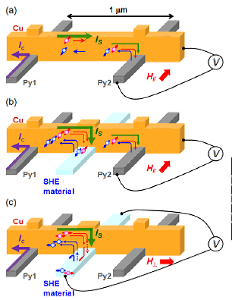
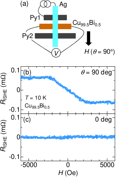
A LSV consists of two ferromagnetic wires and a nonmagnetic wire which bridges the two ferromagnets as shown in Fig. 1(a). In the present paper, we use permalloy (Py; Ni81Fe19) as a ferromagnet and Cu as a nonmagnetic material (except for Fig. 7). When an electric charge current is injected from one of the ferromagnets [Py1 in Fig. 1(a)] into the nonmagnetic material, nonequilibrium spin accumulation is generated at the interface and is relaxed within a certain length, so-called spin diffusion length. Within the spin diffusion length, a pure spin current, which is defined as , can flow only on the right side of the nonmagnetic wire. Here and are spin-up and spin-down currents, respectively. The nonequilibrium spin accumulation can be detected as a nonlocal voltage using the other ferromagnetic wire [Py2 in Fig. 1(a)]. The detected voltage depends on the magnetization of the two ferromagnetic wires, i.e., parallel or antiparallel state. The difference in between the parallel and antiparallel states, i.e., is proportional to the spin accumulation at the position of the Py2 detector. The magnetic field in this case is applied along the easy direction of the ferromagnetic wires (). As detailed in Ref. wakamura_apex_2011, , we can determine the spin diffusion lengths of Py () and Cu () as well as the spin polarization of Py () by plotting as a function of the distance () between Py1 and Py2. In the present study, nm bass_jmmm_1997 ; dubois_prb_1999 ; niimi_prl_2013 , m wakamura_apex_2011 , and niimi_prl_2011 ; niimi_prl_2012 at K.
When a SHE material is inserted just in the middle of Py1 and Py2, the pure spin current generated from Py1 is partly absorbed into the SHE middle wire because of its strong SO interaction, as shown in Fig. 1(b). As a result, the spin accumulation detected at Py2 is reduced. This reduction, i.e., the spin absorption rate , can be expressed as follows niimi_prl_2011 ; niimi_prl_2012 :
| (1) |
where and are the spin accumulation signals ( divided by the injection current ) with and without the SHE middle wire, respectively. and are defined as , and , where , , and are the spin resistances of Py, Cu, and the middle wire, respectively note_spin_resistance . Since only the spin diffusion length of the SHE middle wire is left as an unknown parameter in Eq. (1), it can be obtained by measuring experimentally.
In order to measure the SHE with this device, we need to apply the magnetic field along the hard direction of the Py wires (), as shown in Fig. 1(c). This is related to the fact that the charge current due to the ISHE is proportional to the cross product of and the direction of spin. In this type of SH device, is absorbed into the SHE material perpendicularly [see Fig. 1(c)]. Thus, to obtain a Hall voltage due to the ISHE (), the direction of spin has to be aligned along the hard direction of the Py wires. Based on the 1D spin diffusion model, the SH resistivity , which is directly related to the SH angle, can be written as follows takahashi_review_2008 ; niimi_prl_2011 ; niimi_prl_2012 :
| (2) |
where is the amplitude of the ISHE resistance and is defined as
and are the effective spin current injected vertically into the SHE middle wire and the thickness of the middle wire, respectively. The perpendicularly absorbed pure spin current decreases in the SHE material, exponentially when , linearly down to zero at the bottom of the SHE wire when .
The coefficient in Eq. (2) is so-called the shunting factor. This factor expresses the shunting by the Cu contact above the SHE material and its value, , can be found by additional measurements that have been described in Ref. niimi_prl_2011, . However, as detailed in Ref. liu_arxiv_2011, , there was a debate on how to evaluate the shunting factor . The evaluation of is very crucial to determine the SH angle correctly. As we will see in the next subsection, the shunting is automatically taken into account in the 3D finite element analysis.
II.2 3D model
The detailed explanation of our 3D model extending the 1D Valet-Fert model of spin transport has been presented in the Supplemental Material of our previous work niimi_prl_2012 . Here we focus on how to obtain the spin diffusion length and the SH angle with the 3D model.
Numerical calculations based on the 3D version of the Valet-Fert model have been performed using SpinFlow 3D. It implements a finite element method to solve a discrete formulation of the bulk transport equations, supplemented with the interface and boundary conditions. In SpinFlow 3D, the interface resistance and the spin mixing conductance brataas_prl_2000 between Cu and Py are important parameters. In the present case, we take their values from appropriate references; fm2 from Ref. bass_ass_2009, and m-2 from Refs. taniguchi_apex_2008, and ghosh_prl_2012, . The interface resistance between Cu and a very weakly doped Cu should be very small and we have taken the smallest value found in the literature, 0.1 fm2 [see Ref. bass_review_2007, ].
We first determine the spin polarization and the interfacial resistance asymmetry coefficient values in the Valet-Fert model valet_prb_1993 by fitting the nonlocal spin valve (NLSV) signal without any middle wire as a function of with SpinFlow 3D, as we have done with the 1D model. In our case, at 10 K. is slightly different from from the 1D model. When there is a middle wire in between the two ferromagnetic wires, the spin current is partially absorbed into it, leading to the reduction of the spin accumulation signal at the detector. By choosing an appropriate value in SpinFlow 3D, we can reproduce . In a similar way, we can determine the SH angle . We rotate the magnetization direction of the Py wire in SpinFlow 3D and put an appropriate value for the middle wire. As a result, we can reproduce a vs curve in the simulation. Here we note that the shunting by the Cu contact is automatically taken into account in this 3D finite element calculation.
III Weak antilocalization
As discussed in Sec. II, the spin absorption method is one of the ways to evaluate the spin diffusion length and the SH angle on the same device. Especially, the evaluation of the spin diffusion length is a key issue to estimate the SH angle correctly. However, there was a heavy debate about the evaluation of the spin diffusion length and the SH angle using this method liu_arxiv_2011 ; niimi_prl_2013 . In addition, the spin diffusion length of Pt determined with the spin absorption method morota_prb_2011 is always several times larger than that obtained with nonmagnet/ferromagnet bilayer films liu_prl_2011 ; liu_arxiv_2011 . To judge whether the spin diffusion length obtained with the spin absorption method is too large or not, one needs another approach.
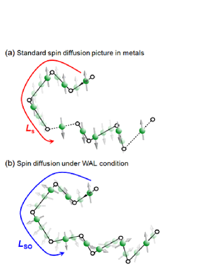
Weak antilocalization (WAL) is one of the simple ways to obtain the spin diffusion length, as already reported in previous papers bass_review_2007 ; niimi_prl_2013 ; bass_review_2013 . Weak localization occurs in metallic systems and has been used to study decoherence of electrons montambaux_book ; pierre_prb_2003 ; niimi_prl_2009 ; niimi_prb_2010 . The principle of this technique relies on constructive interference of closed electron trajectories which are traveled in opposite direction (time reversed paths). This leads to an enhancement of the resistance. The magnetic field perpendicular to the plane destroys these constructive interferences, leading to a negative magnetoresistance whose amplitude and width are directly related to the phase coherence length. If there is a non-negligible SO interaction, a positive magnetoresistance can be obtained, which is referred to as WAL hikami_ptp_1980 .
The dimension of the system is determined with respect to the phase coherence length and the elastic mean free path . Since we deal with nanometer-scale metallic systems, is in general smaller than all the sample dimensions. On the other hand, the inelastic scattering length can be relatively long for a clean metallic system. When is larger than the width and the thickness of the sample but smaller than the length , we call the system “quasi-1D”.
The WAL peak of quasi-1D wire can be fitted by the Hikami-Larkin-Nagaoka formula montambaux_book ; hikami_ptp_1980 :
| (3) |
where , and are the WAL correction factor, the resistance of the wire at high enough field, and the SO length, respectively. and are the reduced Plank constant and the magnetic length, respectively. In Eq. (3), we have only two unknown parameters; and . According to the Fermi liquid theory niimi_prl_2009 ; niimi_prb_2010 ; aak_1982 , depends on temperature (), while is almost constant at low temperatures pierre_prb_2003 .
The relation between the SO length and the spin diffusion length has been theoretically discussed in Ref. zutic_review_2004, and experimentally verified recently by some of the present authors niimi_prl_2013 . The schematics of the two length scales are depicted in Fig. 2. In metallic systems where the Elliott-Yafet mechanism is dominant ey , the following relation can be lead;
| (4) |
Since is basically equivalent to or , we use hereafter only or as the spin diffusion length of nonmagnetic metal.
IV Sample fabrication and experimental setup
Our SH device is based on a LSV structure where a SHE material is inserted in between two Py wires and bridged by a Cu wire, as shown in Fig. 1. Samples were patterned using electron beam lithography onto a thermally oxidized silicon substrate coated with polymethyl-methacrylate (PMMA) resist for depositions of Py, Cu, Ag, Au, and CuPb alloys, or coated with ZEP 520A resist for depositions of CuBi and AgBi.
A pair of Py wires was first deposited using an electron beam evaporator under a base pressure of 10-9 Torr. The width and thickness of the Py wires are 100 and 30 nm, respectively. The CuBi, AgBi and CuPb middle wires were next deposited by magnetron sputtering with Bi-doped Cu and Ag targets and Pb-doped Cu targets, respectively. The Bi concentrations used in this work were 0%, 0.3%, and 0.5% for CuBi, and 0%, 1%, and 3% for AgBi. As for CuPb, we used only 0.5% of Pb in Cu. We also prepared Au middle wires since the spin diffusion length of Au is expected to be as long as that of CuBi. The Au wires were deposited by a Joule heating evaporator using a 99.997% purity source. The width and thickness of CuBi, AgBi and CuPb are 250 and 20 nm (except for Fig. 5) while those of Au are 200 and 20 nm.
The post-baking temperature for the PMMA resist was kept below 90 ∘C after the deposition of CuBi, AgBi or CuPb alloys. Bismuth and lead have low melting temperatures (270 ∘C and 330 ∘C), which oblige us to use a much lower post-baking temperature. We have confirmed that the post-baking temperature of 90 ∘C does not change the resistivities of CuBi, AgBi, and CuPb wires. Before deposition of a Cu bridge, we performed a careful Ar ion beam etching for 30 seconds in order to clean the surfaces of Py and the SHE middle wires. After the Ar ion etching, the device was moved to another chamber without breaking a vacuum and subsequently the Cu bridge was deposited by a Joule heating evaporator using a 99.9999% purity source. For comparison, we also prepared similar SH devices but bridged by a Ag wire from a 99.999% purity source. Both the width and thickness of Cu (or Ag in Fig. 7) are 100 nm.
For the WAL samples, we prepared 1 mm long and 100 nm wide Au wires, and 120 nm wide Cu99.7Bi0.3 and Cu99.5Bi0.5 wires. The thickness is 20 nm, which is the same as in the SHE device.
The measurements have been carried out using an ac lock-in amplifier (modulation frequency Hz) and a 4He flow cryostat. In order to obtain a very small WAL signal compared to the background resistance, we used a bridge circuit as detailed in Ref. niimi_prb_2010, . To check the reproducibility and to evaluate the error bar (see Table 1), we have measured at least a few different samples from the same batch.
V Experimental results and discussions
V.1 SHEs of CuBi and Au
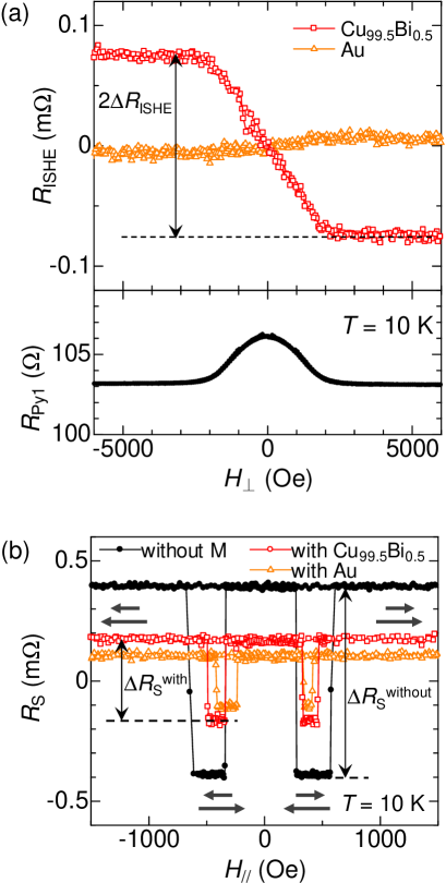
We first compare two ISHE resistances, i.e., of Cu99.5Bi0.5 and Au measured at K in Fig. 3(a). As already explained in Sec. II A, in our device structure, linearly increases with increasing the magnetic field and it is saturated above 2000 Oe which is the saturation field of the magnetization. This saturation field can be confirmed from the anisotropic magnetoresistance (AMR) curve of Py1 in the lower panel of Fig. 3(a). Although the sign of of Cu99.5Bi0.5 is opposite to that of Au, its amplitude is more than 10 times larger compared to that of Au.
To evaluate the spin absorption rate and the spin diffusion length of the middle wire, we performed NLSV measurements with and without the middle wire. Figure 3(b) shows NLSV signals with the Cu99.5Bi0.5 and Au middle wires, and also without any middle wire as a reference signal. Apparently, the insertion of the SHE materials in the LSV structure induces the reduction in detected at Py2. By using the 1D and 3D spin transport models, the spin diffusion lengths of Cu99.5Bi0.5 and Au can be obtained and are listed in Table 1. Both and of Cu99.5Bi0.5 are almost the same as and of Au, respectively. As already pointed out in Ref. niimi_prl_2012, and will be detailed later on, when , the 1D model underestimates not only but also compared to the 3D model.
| SHE material | method | or | |||||
|---|---|---|---|---|---|---|---|
| (20 nm) | (cm) | (nm) | (nm) | (nm) | |||
| Au | LSV & WAL | 4.0 | |||||
| Cu99.7Bi0.3 | LSV & WAL | 3.2 | |||||
| Cu99.5Bi0.5 | LSV & WAL | 5.1 | |||||
| Cu99.5Pb0.5 | LSV | 5.4 | - | ||||
| Ag99Bi1 | LSV | 6.8 | - | ||||
| Cu99Ir1 [niimi_prl_2011, ] | LSV | 3.1 | - | ||||
| Pt [niimi_prl_2013, ] | LSV & WAL | 10 | |||||
| Ta [morota_prb_2011, ] | LSV | 330 | - |
Concerning the SH angles, we obtain for Cu99.5Bi0.5, if we divide by the Bi-induced resistivity . This is based on the fact that the ISHE cannot be detected for pure Cu wire and the resistivity of pure Cu wire is not negligibly small compared to the total resistivity . If is divided by , the SH angle of Cu99.5Bi0.5 becomes as already pointed out in Ref. niimi_prl_2012, . On the other hand, of 20 nm thick Au is . This SH angle is consistent with the values reported in some previous works with comparable Au thicknesses hoffmann_prl_2009 ; hoffmann_prl_2010 ; hoffmann_prb_2010 ; bogu_prl_2010 ; takanashi_mrs_2012 .
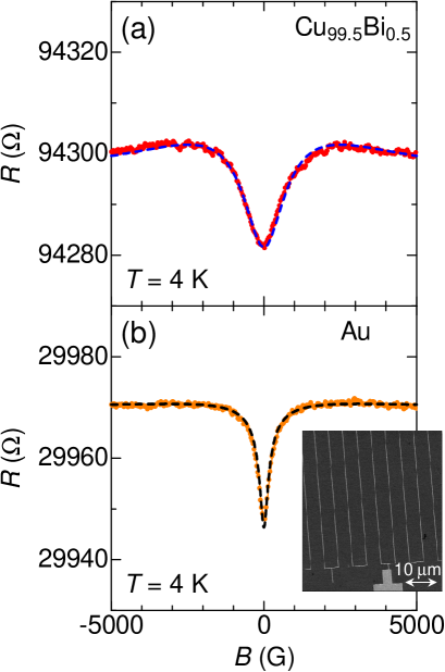
In order to double-check obtained from the spin absorption measurements, we prepared simple Cu99.5Bi0.5 and Au wires, and performed WAL measurements at K as shown in Fig. 4. For both wires, clear positive magnetoresistance is observed, which is typical of WAL. By fitting the WAL curves with Eq. (3), can be obtained and converted into using Eq. (4). As can be seen in Table 1, the obtained of Cu99.7Bi0.3, Cu99.5Bi0.5 and Au are quantitatively consistent with from the spin absorption measurements. Thus, it turns out that the WAL method is valid to evaluate the spin diffusion length quantitatively not only for pure metals such as Pt niimi_prl_2013 and Au but also for dilute alloys.
V.2 Thickness dependence of SHE of CuBi
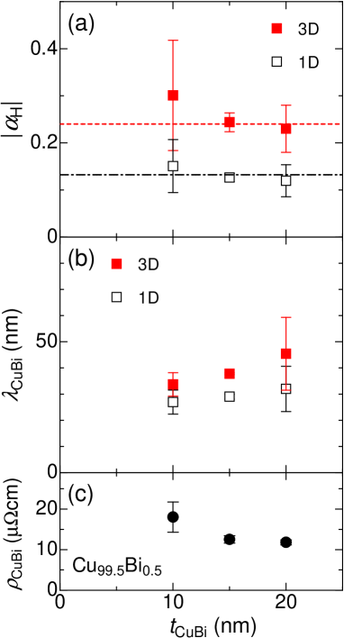

Next we study the thickness dependence of the SHE of Cu99.5Bi0.5. Figure 5 shows the thickness dependence of (a) the SH angle, (b) the spin diffusion length, and (c) the resistivity of the Cu99.5Bi0.5 middle wire. With decreasing , the SH angle slightly increases but not so drastically compared to the case of -tungsten ralph_apl_2013 . If we assume that the SH angle is independent of below 20 nm, we obtain , which is consistent with the value estimated from the Bi concentration dependence niimi_prl_2012 . This almost independent with respect to indicates that the ISHE signal originates from the skew scattering from homogenously distributed Bi impurities in the Cu wire. On the other hand, the spin diffusion length decreases with decreasing the thickness as shown in Fig. 5(b). This tendency can be qualitatively understood by the resistivity change [see Fig. 5(c)], as reported in our previous work niimi_prl_2013 where the spin diffusion length of Cu is inversely proportional to its resistivity.
As already shown in Ref. niimi_prl_2012, , the spreading of the spin accumulation at the side edges of the SHE material wire leads to the underestimations of and when . In Fig. 6, we show 3D mappings of the spin accumulation voltage for (a) 10 nm thick Cu99.5Bi0.5, (b) 20 nm thick Cu99.5Bi0.5, and (c) 20 nm thick Au devices. The corresponding are also plotted in Figs. 6(d)-6(f). For both Cu99.5Bi0.5 and Au middle wires, the spreading of the spin accumulation can be seen since the spin diffusion lengths of Cu99.5Bi0.5 and Au are larger than . This is the reason for the difference between and as well as the difference between and . Compared to the 20 nm thick Cu99.5Bi0.5 device, the spreading of the spin accumulation is smaller for the 10 nm thick Cu99.5Bi0.5 device [see Figs. 6(a) and 6(b)], although are almost the same for the two devices [see Figs. 6(d) and 6(e)]. This comes from the thickness dependence of the spin diffusion length, i.e., smaller for thinner , as shown in Fig. 5(b).
V.3 SHEs of several different materials
In this subsection, we discuss the extrinsic SHEs measured with other material combinations. We first substituted Ag for the Cu bridge as illustrated in Fig. 7(a). Figure 7(b) shows of a 20 nm thick Cu99.5Bi0.5 wire bridged by a 100 nm thick Ag wire. As for the amplitude , it is slightly smaller than that in Fig. 3(a). This might be related to a slightly smaller spin diffusion length of a 100 nm thick Ag wire compared to Cu idzuchi_apl_2012 , although we did not check the dependence of the NLSV signal without any middle wire. The sign of is also negative for . Note that is defined as . We then changed the magnetic field angle to confirm if the observed signal for the Ag bridge really comes from the ISHE of the Cu99.5Bi0.5 wire. The signal disappears when [see Fig 7(b)] and the sign reverses when . These results clearly show that does not depend on the bridge material which is used to transfer the pure spin current to the middle wire.
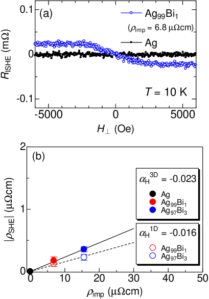
Next we keep the Cu bridge and change the host metal from Cu to Ag since Bi-doped Ag is also predicted to have a large SHE gradhand_prl_2010 ; gradhand_prb_2010 . In Fig. 8(a), we show of Ag99Bi1 and pure Ag measured at K. Apparently, when there is no Bi impurity in Ag, no ISHE is observed, which means that is negligibly small in pure Ag. This result is consistent with a recent spin pumping measurement with Ag/Py bilayer films vila_nat_commun_2013 . Once a small amount of Bi impurities is added in Ag, a negative ISHE is observed as shown in Fig. 8(a). Contrary to the theoretical predictions gradhand_prl_2010 ; gradhand_prb_2010 , however, the observed ISHE of Ag99Bi1 was not so large as that of Cu99.5Bi0.5 [see Fig. 1(a)].
To determine the SH angle of AgBi alloys, we plot as a function of . As can be seen in Fig. 8(b), linearly increases with increasing the Bi concentration up to 3%, which clearly shows that the skew scattering is the dominant mechanism for the SHE niimi_prl_2011 . This result also indicates that there is no segregation of Bi in Ag up to 3%, while Bi impurities start to segregate from 0.5% in Cu as already discussed in Ref. niimi_prl_2012, . Using the 1D and 3D models, and can be estimated as and , respectively. Compared to CuBi alloys, the SH angle is one order smaller and comparable to that of CuIr alloys niimi_prl_2011 ; niimi_prl_2012 .
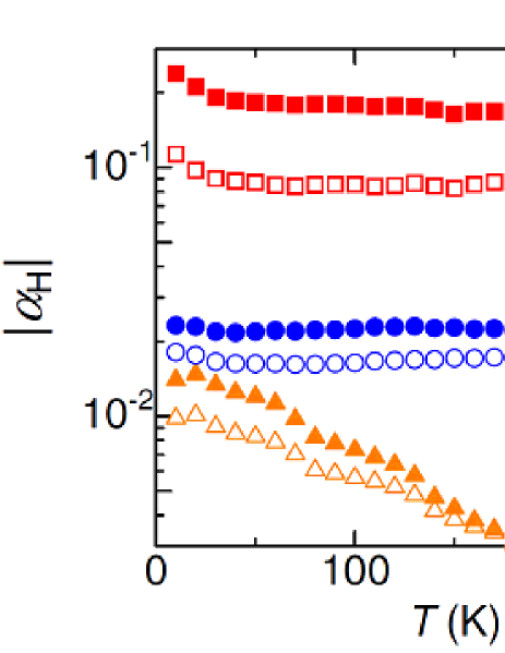
So far, we have fixed the temperature at K where the phonon contribution can be neglected. To see the temperature dependence of the SH angle is one of the best ways to discuss the dominant mechanism of the SHE jin_prl_2009 . For this purpose, we measured and every 10 K, and estimated and . Figure 9 shows the temperature dependence of the absolute values of and for Cu99.5Bi0.5, Ag99Bi1, and Au. Ag99Bi1 has an almost temperature independent SH angle, which is characteristic of the skew scattering niimi_prl_2011 ; jin_prl_2009 , and the difference between and is relatively small. Cu99.5Bi0.5 has almost the same tendency as Ag99Bi1 although there is a slight enhancement of the SH angle below 30 K.
As for Au, on the other hand, the temperature dependence of the SH angle is quite different from those of the other two alloys. Both and decrease with increasing temperature and the difference between the two is getting smaller. The temperature dependence of the SHE of noble metal has been discussed in Pt vila_prl_2007 ; kajiwara_j_phys_2009 as well as in Au kajiwara_j_phys_2009 . In Ref. vila_prl_2007, , it was found that the SH conductivity of Pt is independent of temperature, which means that the SH angle increases with increasing temperature. The same tendency has been confirmed in the inverse SH voltage for a Pt/Py bilayer film kajiwara_j_phys_2009 . On the other hand, in the case of Au, the temperature dependence is opposite to the case of Pt kajiwara_j_phys_2009 , which is consistent with the present result. In Refs. vila_prl_2007, and kajiwara_j_phys_2009, , such a temperature dependence was attributed to the two extrinsic contributions, namely skew scattering and side jump. However, as already shown in a few theoretical guo_prl_2008 ; tanaka_prb_2008 and experimental papers jin_prl_2009 , the linearly increasing or decreasing SH angle with temperature is typical of the intrinsic mechanism based on the degeneracy of orbits by SO coupling. In the present case, the intrinsic mechanism is predominant since the SH angle decreases almost linearly with increasing temperature, which is qualitatively different from Ref. seki_nat_mater_2008, where the SH angle of Au is independent of temperature, characteristic of the skew scattering.
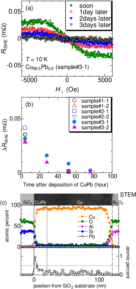
We now come back to the Cu host and change the impurity. What happens when another 6 impurity is doped in Cu? We fabricated SH devices using Cu99.5Pb0.5 and measured the ISHE and NLSV at K. In Fig. 10(a), we show of Cu99.5Pb0.5. Note that all Cu99.5Pb0.5 samples were prepared within five hours after the deposition of CuPb middle wires. When we measure the Cu99.5Pb0.5 samples right after the deposition of the Cu bridge, it has two times smaller than Cu99.5Bi0.5, while the spin diffusion length of Cu99.5Pb0.5 is comparable or even larger than that of Cu99.5Bi0.5 [see Table 1]. From the ISHE and NLSV measurements, of Cu99.5Pb0.5 is estimated to be , which is half of of Cu99.5Bi0.5.
What is interesting to note is the aging effect of of Cu99.5Pb0.5. After the measurements at K, the samples were warmed up to room temperature and kept in a vacuum box for 1 day. Then we measured the same samples again at K. As can be seen in Fig. 10(a), of Cu99.5Pb0.5 decreases by more than half. We simply repeated this procedure until we could not obtain . In a few days, of Cu99.5Pb0.5 disappeared. On the other hand, Cu99.5Bi0.5 did not show such an aging effect at least in one week. In Fig. 10(b), we plot of Cu99.5Pb0.5 as a function of time after the deposition of the CuPb wire. For six samples from three different batches, disappears within a few days.
The above result indicates that Pb impurities in the middle wire move somewhere. In fact, it is known that Pb has a very fast mobility. According to a scanning tunneling microscopy study on Cu islands on Pb(111) substrate stm_lead , Cu islands are masked by Pb atoms from the substrate. This migration originates from a very fast mobility of Pb in Cu. We have taken a scanning tunneling electron microscopy (STEM) image of the Cu99.5Pb0.5 and Cu junction and performed energy dispersive x-ray (EDX) analyses several days after the deposition of CuPb wire. In our procedure, we cannot take the STEM image right after the CuPb deposition, but as shown in Fig. 10(c), Pb atoms are segregated at the bottom of the middle wire several days after the fabrication. Presumably, such segregated Pb impurities at the substrate would not contribute to the ISHE, and thus of Cu99.5Pb0.5 becomes almost zero in a few days.
Before closing this subsection, we discuss the reason why 6 impurities such as Pb and Bi in the Cu host show large SH angles. First of all, Pb and Bi have large SO interactions because of their large atomic numbers. According to recent theoretical predictions gradhand_prl_2010 ; gradhand_prb_2010 , a large difference of SO interactions between the host (in the present case, Cu) and impurity metals is one of the key points to have a large SHE based on the skew scattering mechanism. In addition, not only the atomic number but also the orbit of outermost shell play an important role in the strength of SO interaction orbit_vs_SO . Intuitively thinking, when the orbital angular momentum is large, the SO interaction is also large. However, to obtain the expectation value of SO interaction, one needs to multiply the wave functions. When the orbital angular momentum is large ( or orbits), the wave function is rather closed and does not have a chance to hybridize with the most outer orbit. On the other hand, orbits have spread wave functions and thus have larger SO interactions orbit_vs_SO . Therefore, 6 impurities such as Pb and Bi have the largest SO interactions. For CuBi, a calculation based on a phase shift model predicts a negative SH angle but smaller () than the experimental one. A similar calculation has not been performed for AgBi and CuPb.
V.4 SHE of Ta
Finally, let us mention the spin diffusion length and the SH angle of Ta. This topic was the cause of the big debate among several groups liu_arxiv_2011 . In Ref. morota_prb_2011, , some of the present authors reported and of Ta using the 1D models, i.e., Eqs. (1) and (2), respectively. However, according to Ref. liu_science_2012, , the SH angle of Ta is , which is about 40 times larger than our of Ta. Liu et al. pointed out in Ref. liu_arxiv_2011, that the overestimations of the shunting factor and result in a large underestimation of the SH angle of Ta. Thus, we have performed the 3D analysis to obtain and of Ta. As can be seen in Table 1, is 3 nm, which is the same as . On the other hand, is which is twice larger than . This difference certainly comes from the overestimation of . However, the large SH angle reported in Ref. liu_science_2012, cannot be reproduced in our analysis. The big difference in of Ta between Ref. liu_science_2012, and the present result is not clear yet, but apparently it does not originate from the overestimation of the spin diffusion length of Ta. We believe that in the ferromagnetic/Ta bilayer system, some additional effects are induced at the interface between Ta and the ferromagnet ohno_nat_mater_2013 , and thus the SH angle obtained in Ref. liu_science_2012, is seemingly enhanced by a factor of more than 10.
VI Conclusions
We have experimentally studied the extrinsic SHEs of CuBi, AgBi, and CuPb alloys with the spin absorption technique in the lateral spin valve structure. Among them, CuBi shows the largest SHE. The SH angle estimated with the 3D model amounts to . Such a large SHE of CuBi has been supported by several additional measurements; (i) comparison with the SHE of Au which has a comparable spin diffusion length to CuBi, (ii) WAL measurements to obtain the spin diffusion length, (iii) the CuBi thickness dependence of the SH angle, (iv) ISHE measurements with substitution of Ag for the Cu bridge, and (v) the magnetic field angle dependence of the ISHEs. CuPb also shows a large SH angle () but the SH signal disappears in a few days presumably because of the fast migration of Pb in Cu. On the other hand, when the Cu host is replaced with Ag, the SH angle is reduced by a factor of ten.
Acknowledgements.
We acknowledge helpful discussions with S. Maekawa, B. Gu, J. Bass, W. P. Pratt, T. Kato, Y. Yanase, H. Harima, and K. Kondou. We would also like to thank Y. Iye and S. Katsumoto for the use of the lithography facilities. This work was supported by KAKENHI (Grant No. 22840012, 24740217, and 23244071).References
- (1) S. Maekawa, Concepts in Spin Electronics (Oxford University Press, Oxford, 2006).
- (2) K. Uchida, S. Takahashi, K. Harii, J. Ieda, W. Koshibae, K. Ando, S. Maekawa, and E. Saitoh, Nature (London) 455, 778 (2008).
- (3) K. Uchida, J. Xiao, H. Adachi, J. Ohe, S. Takahashi, J. Ieda, T. Ota, Y. Kajiwara, H. Umezawa, H. Kawai, G. E. W. Bauer, S. Maekawa, and E. Saitoh, Nat. Mater. 9, 894 (2010).
- (4) K. Uchida, H. Adachi, T. An, T. Ota, M. Toda, B. Hillebrands, S. Maekawa, and E. Saitoh, Nat. Mater. 10, 737 (2011).
- (5) A. Kirihara, K. Uchida, Y. Kajiwara, M. Ishida, Y. Nakamura, T. Manako, E. Saitoh, and S. Yorozu, Nat. Mater. 11, 686 (2012).
- (6) D. Qu, S. Y. Huang, Jun Hu, Ruqian Wu, and C. L. Chien, Phys. Rev. Lett. 110, 067206 (2013).
- (7) T. Kikkawa, K. Uchida, Y. Shiomi, Z. Qiu, D. Hou, D. Tian, H. Nakayama, X.-F. Jin, and E. Saitoh, Phys. Rev. Lett. 110, 067207 (2013).
- (8) L. Liu, C.-F. Pai, Y. Li, H. W. Tseng, D. C. Ralph, and R. A. Buhrman, Science 336, 555 (2012).
- (9) L. Liu, O. J. Lee, T. J. Gudmundsen, D. C. Ralph, and R. A. Buhrman, Phys. Rev. Lett. 109, 096602 (2012).
- (10) G. Y. Guo, S. Murakami, T.-W. Chen, and N. Nagaosa, Phys. Rev. Lett. 100, 096401 (2008).
- (11) T. Tanaka, H. Kontani, M. Naito, T. Naito, D. S. Hirashima, K. Yamada, and J. Inoue, Phys. Rev. B 77, 165117 (2008).
- (12) M. Morota, Y. Niimi, K. Ohnishi, D. Wei, T. Tanaka, H. Kontani, T. Kimura, and Y. Otani, Phys. Rev. B 83, 174405 (2011).
- (13) J. Smit, Physica (Amsterdam) 24, 39 (1958).
- (14) L. Berger, Phys. Rev. B 2, 4559 (1970).
- (15) M. Gradhand, D. V. Fedorov, P. Zahn, and I. Mertig, Phys. Rev. Lett. 104, 186403 (2010).
- (16) M. Gradhand, D. V. Fedorov, P. Zahn, and I. Mertig, Phys. Rev. B 81, 245109 (2010).
- (17) A. Fert and P. M. Levy, Phys. Rev. Lett. 106, 157208 (2011).
- (18) Y. Niimi, M. Morota, D. Wei, C. Deranlot, M. Basletic, A. Hamzic, A. Fert, and Y. Otani, Phys. Rev. Lett. 106, 126601 (2011).
- (19) Y. Niimi, Y. Kawanishi, D. Wei, C. Deranlot, H. Yang, M. Chshiev, T. Valet, A. Fert, and Y. Otani, Phys. Rev. Lett. 109, 156602 (2012).
- (20) M. Yamanouchi, L. Chen, J. Kim, M. Hayashi, H. Sato, S. Fukami, S. Ikeda, F. Matsukura, and H. Ohno, Appl. Phys. Lett. 102, 212408 (2013).
- (21) E. Saitoh, M Ueda, H. Miyajima, and G. Tatara, Appl. Phys. Lett. 88, 182509 (2006).
- (22) O. Mosendz, J. E. Pearson, F. Y. Fradin, G. E. W. Bauer, S. D. Bader, and A. Hoffmann, Phys. Rev. Lett. 104, 046601 (2010).
- (23) O. Mosendz, V. Vlaminck, J. E. Pearson, F. Y. Fradin, G. E. W. Bauer, S. D. Bader, and A. Hoffmann, Phys. Rev. B 82, 214403 (2010).
- (24) L. Liu, T. Moriyama, D. C. Ralph, and R. A. Buhrman, Phys. Rev. Lett. 106, 036601 (2011).
- (25) K. Kondou, H. Sukegawa, S. Mitani, K. Tsukagoshi, and S. Kasai, Appl. Phys. Express 5, 073002 (2012).
- (26) H. Nakayama, M. Althammer, Y.-T. Chen, K. Uchida, Y. Kajiwara, D. Kikuchi, T. Ohtani, S. Geprags, M. Opel, S. Takahashi, R. Gross, G. E. W. Bauer, S. T. B. Goennenwein, E. Saitoh, Phys. Rev. Lett. 110, 206601 (2013).
- (27) S. O. Valenzuela and M. Tinkham, Nature (London) 442, 176 (2006).
- (28) T. Seki, Y. Hasegawa, S. Mitani, S. Takahashi, H. Imamura, S. Maekawa, J. Nitta and K. Takanashi, Nat. Mater. 7, 125 (2008).
- (29) G. Mihajlović, J. E. Pearson, M. A. Garcia, S. D. Bader, and A. Hoffmann, Phys. Rev. Lett. 103, 166601 (2009).
- (30) B. Gu, I. Sugai, T. Ziman, G.Y. Guo, N. Nagaosa, T. Seki, K. Takanashi, and S. Maekawa, Phys. Rev. Lett. 105, 216401 (2010).
- (31) K. Takanashi, S. Shibata, I. Sugai and T. Seki, MRS Proceedings 1458 (2012); doi:10.1557/opl.2012.1350.
- (32) S. Takahashi and S. Maekawa, Phys. Rev. B 67, 052409 (2003).
- (33) S. Takahashi and S. Maekawa, Sci. Tech. Adv. Mater. 9, 014105 (2008).
- (34) T. Valet and A. Fert, Phys. Rev. B 48, 7099 (1993).
- (35) L. Liu, R. A. Buhrman, and D. C. Ralph, arXiv:1111.3702.
- (36) T. Wakamura, K. Ohnishi, Y. Niimi, and Y. Otani, Appl. Phys. Express 4, 063002 (2011).
- (37) S. D. Steenwyk, S. Y. Hsu, R. Loloee, J. Bass, W. P. Pratt Jr., J. Magn. Magn. Mater. 170, L1 (1997).
- (38) S. Dubois, L. Piraux, J. George, K. Ounadjela, J. Duvail, and A. Fert, Phys. Rev. B 60, 477 (1999).
- (39) Y. Niimi, D. Wei, H. Idzuchi, T. Wakamura, T. Kato, and Y. Otani, Phys. Rev. Lett. 110, 016805 (2013).
- (40) The spin resistance of material “X” (N, F, or M), i.e., , is defined as , where , , and are respectively the electrical resistivity, the spin diffusion length, the spin polarization, and the effective cross sectional area involved in the equations of the 1D spin diffusion model. See Ref. niimi_prl_2012, for more details.
- (41) A. Brataas, Y. V. Nazarov, and G. E. W. Bauer, Phys. Rev. Lett. 84, 2481 (2000).
- (42) W. Pratt and J. Bass, Appl. Surf. Sci. 256, 399 (2009).
- (43) T. Taniguchi, S. Yakata, H. Imamura, and Y. Ando, Appl. Phys. Express 1, 031302 (2008).
- (44) A. Ghosh, S. Auffret, U. Ebels, and W. E. Bailey, Phys. Rev. Lett. 109, 127202 (2012).
- (45) J. Bass and W. P. Pratt, J. Phys.; Condes. Matter 19, 183201 (2007).
- (46) J. Bass, arXiv:1305.3848.
- (47) E. Akkermans and G. Montambaux, Mesoscopic Physics of Electrons and Photons (Cambridge University Press, Cambridge, England, 2007).
- (48) F. Pierre, A. Gougam, A. Anthore, H. Pothier, D. Esteve, and N. Birge, Phys. Rev. B 68, 085413 (2003).
- (49) Y. Niimi, Y. Baines, T. Capron, D. Mailly, F.-Y. Lo, A. Wieck, T. Meunier, L. Saminadayar, and C. Bäuerle, Phys. Rev. Lett. 102, 226801 (2009).
- (50) Y. Niimi, Y. Baines, T. Capron, D. Mailly, F.-Y. Lo, A. Wieck, T. Meunier, L. Saminadayar, and C. Bäuerle, Phys. Rev. B 81, 245306 (2010).
- (51) S. Hikami, A. I. Larkin, Y. Nagaoka, Prog. Theor. Phys. 63, 707 (1980).
- (52) B. L. Altshuler, A. G. Aronov, and D. E. Khmelnitsky, J. Phys. C 15, 7367 (1982).
- (53) I. Zŭtić, J. Fabian, and S. Das Sarma, Rev. Mod. Phys. 76, 323 (2004).
- (54) R. J. Elliott, Phys. Rev. 96, 266 (1954); Y. Yafet, in Solid State Physics, edited by F. Sitz and D. Turnbull (Academic, New York, 1963), Vol. 14.
- (55) C.-F. Pai, L. Liu, Y. Li, H. W. Tseng, D. C. Ralph, and R. A. Buhrman, Appl. Phys. Lett. 101, 122404 (2012).
- (56) H. Idzuchi, Y. Fukuma, L. Wang, and Y. Otani, Appl. Phys. Lett. 101, 022415 (2012).
- (57) J. C. Rojas Sánchez, L. Vila, G. Desfonds, S. Gambarelli, J. P. Attané, J. M. De Teresa, C. Magén, and A. Fert, Nat. Commun. 4, 2944 (2013).
- (58) Y. Tian, L. Ye, and X.-F. Jin, Phys. Rev. Lett. 103, 087206 (2009).
- (59) L. Vila, T. Kimura, and Y. Otani, Phys. Rev. Lett. 99, 226604 (2007).
- (60) Y. Kajiwara, K. Ando, K. Sasage, and E. Saitoh, J. Phys.: Conf. Ser. 150, 042080 (2009).
- (61) C. Nagl, E. Platzgummer, M. Schmid, P. Varga, S. Speller and W. Heiland, Phys. Rev. Lett. 75, 2976 (1995).
- (62) Y. Yanase and H. Harima, Kotai Butsuri 46, 229 (2011) (in Japanese).
- (63) J. Kim, J. Sinha, M. Hayashi, M. Yamanouchi, S. Fukami, T. Suzuki, S. Mitani, and H. Ohno, Nat. Mater. 12, 240 (2013).