Damping of Terahertz Plasmons in Graphene
Coupled with Surface Plasmons in Heavily-Doped Substrate
Abstract
Coupling of plasmons in graphene at terahertz (THz) frequencies with surface plasmons in a heavily-doped substrate is studied theoretically. We reveal that a huge scattering rate may completely damp out the plasmons, so that proper choices of material and geometrical parameters are essential to suppress the coupling effect and to obtain the minimum damping rate in graphene. Even with the doping concentration cm-3 and the thickness of the dielectric layer between graphene and the substrate nm, which are typical values in real graphene samples with a heavily-doped substrate, the increase in the damping rate is not negligible in comparison with the acoustic-phonon-limited damping rate. Dependence of the damping rate on wavenumber, thicknesses of graphene-to-substrate and gate-to-graphene separation, substrate doping concentration, and dielectric constants of surrounding materials are investigated. It is shown that the damping rate can be much reduced by the gate screening, which suppresses the field spread of the graphene plasmons into the substrate.
I Introduction
Plasmons in two-dimensional electron gases (2DEGs) can be utilized for terahertz (THz) devices. THz sources and detectors based on compound semiconductor heterostructures have been extensively investigated both experimentally and theoretically 1; 2; 3; 4; 5; 6; 7; 8. The two-dimensionality, which gives rise to the wavenumber-dependent frequency dispersion, and the high electron concentration on the order of cm-2 allow us to have their frequency in the THz range with submicron channel length. Most recently, a very high detector responsivity of the so-called asymmetric double-grating-gate structure based on an InP-based high-electron-mobility transistor was demonstrated 9. However, resonant detection as well as single-frequency coherent emission have not been accomplished so far at room temperature, mainly owning to the damping rate more than s-1 in compound semiconductors.
Plasmons in graphene have potential to surpass those in the heterostructures with 2DEGs based on the standard semiconductors, due to its exceptional electronic properties 10. Massive experimental and theoretical works have been done very recently on graphene plasmons in the THz and infrared regions (see review papers Refs. 11; 12 and references therein). One of the most important advantages of plasmons in graphene over those in heterostructure 2DEGs is much weaker damping rate close to s-1 at room temperature in disorder-free graphene suffered only from acoustic-phonon scattering 13. That is very promising for the realization of the resonant THz detection 14 and also of plasma instabilities, which can be utilized for the emission. In addition, interband population inversion in the THz range was predicted 15; 16, and it has been investigated for the utilization not only in THz lasers in the usual sense but also in THz active plasmonic devices 17; 18 and metamaterials 19.
Many experimental demonstrations of graphene-based devices have been performed on graphene samples with heavily-doped substrates, in order to tune the carrier concentration in graphene by the substrate as a back gate. Typically, either peeling or CVD graphene transferred onto a heavily-doped p+-Si substrate, with a SiO2 dielectric layer in between, is used (some experiments on graphene plasmons have adapted undoped Si/SiO2 substrates 20; 21). Graphene-on-silicon, which is epitaxial graphene on doped Si substrates 22, is also used. For realization of THz plasmonic devices, properties of plasmons in such structures must be fully understood. Although the coupling of graphene plasmons to surface plasmons in perfectly conducting metallic substrates with/without dielectric layers in between have been theoretically studied 23; 24, the influence of the carrier scattering in a heavily-doped semiconductor substrate (with finite complex conductivity) has not been taken into account so far. Since the scattering rate in the substrate increases as the doping concentration increases, it is anticipated that the coupling of graphene plasmons to surface plasmons in the heavily-doped substrate causes undisired increase in the damping rate.
The purpose of this paper is to study theoretically the coupling between graphene plasmons and substrate surface plasmons in a structure with a heavily-doped substrate and with/without a metallic top gate. The paper is organized as follows. In the Sec. II, we derive a dispersion equation of the coupled modes of graphene plasmons and substrate surface plasmons. In Sec. III, we study coupling effect in the ungated structure, especially the increase in the plasmon damping rate due to the coupling and its dependences on the doping concentration, the thickness of graphene-to-substrate separation, and the plasmon wavenumber. In Sec. IV, we show that the coupling in the gated structures can be less effective due to the gate screening. We also compare the effect in structures having different dielectric layers between the top gate, graphene layer, and substrate, and reveal the impact of values of their dielectric constants. In Sec. V, we discuss and summarize the main results of this paper.
II Equations of The Model
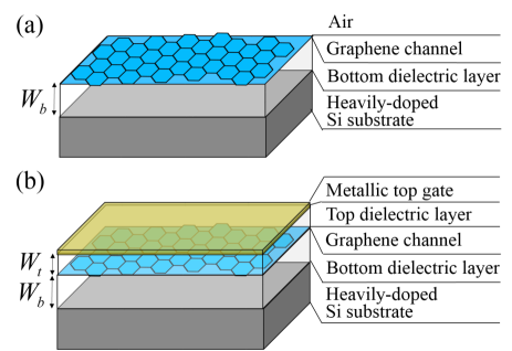
We investigate plasmons in an ungated graphene structure with a heavily-doped p+-Si substrate, where the graphene layer is exposed on the air, as well as a gated graphene structure with the substrate and a metallic top gate, which are schematically shown in Figs. 1(a) and (b), respectively. The thickness of the substrate is assumed to be sufficiently larger than the skin depth of the substrate surface plasmons. The top gate can be considered as perfectly conducting metal, whereas the heavily-doped Si substrate is characterized by its complex dielectric constant.
Here, we use the hydrodynamic equations to describe the electron motion in graphene 26, while using the simple Drude model for the hole motion in the substrate (due to virtual independence of the effective mass in the substrate on the electron density, in contrast to graphene). In addition, these are accompanied by the self-consistent 2D Poisson equation (The formulation used here almost follows that for compound semiconductor high-electron-mobility transistors, see Ref. 25). Differences are the hydrodynamic equations accounting for the linear dispersion of graphene and material parameters of the substrate and dielectric layers. In general, the existence of both electrons and holes in graphene results in various modes such as electrically passive electron-hole sound waves in intrinsic graphene as well as in huge damping of electrically active modes due to the electron-hole friction, as discussed in Ref. 26. Here, we focus on the case where the electron concentration is much higher than the hole concentration and therefore the damping associated with the friction can be negligibly small. Besides, for the generalization purpose, we formulate the plasmon dispersion equation for the gated structure; that for the ungated structure can be readily found by taking the limit (see Fig. 1).
Then, assuming the solutions of the form , where and are the plasmon wavenumber and frequency ( denotes the wavelength), the 2D Poisson equation coupled with the linearized hydrodynamic equations can be expressed as follows:
| (1) |
where is the ac (signal) component of the potential, , , and are the steady-state electron concentration, the hydrodynamic “fictitious mass”, and the collision frequency in graphene, respectively, and is the dielectric constant which is different in different layers. The electron concentration and fictitious mass are related to each other through the electron Fermi level, , and electron temperature, :
| (2) |
| (3) |
In the following we fix and treat the fictitious mass as a function of . The dielectric constant can be represented as
| (4) |
where , , and are the static dielectric constants of the top and bottom dielectric layers and the substrate, respectively, is the bulk plasma frequency in the substrate with and being the doping concentration and hole effective mass, and is the collision frequency in the substrate, which depends on the doping concentration. The dielectric constant in the substrate is a sum of the static dielectric constant of Si, and the contribution from the Drude conductivity. The dependence of the collision frequency, , on the doping concentration, , is calculated from the experimental data for the hole mobility at room temperature in Ref. 27.
We use the following boundary conditions: vanishing potential at the gate and far below the substrate, and ; continuity conditions of the potential at interfaces between different layers, and ; a continuity condition of the electric flux density at the interface between the bottom dielectric layer and the substrate in the -direction, ; and a jump of the electric flux density at the graphene layer, which can be derived from Eq. (1). Equation (1) together with these boundary conditions yield the following dispersion equation
| (5) |
where
| (6) | |||
| (7) | |||
| (8) |
| (9) |
| (10) |
and . In Eq. (5), the term on the right-hand side represents the coupling between graphene plasmons and substrate surface plasmons. If were zero, the equations and would give independent dispersion relations for the former and latter, respectively. Qualitatively, Eq. (8) indicates that the coupling occurs unless or , i.e., unless the separation of the graphene channel and the substrate is sufficiently large or the gate screening of graphene plasmons is effective. Note that the non-constant frequency dispersion of the substrate surface plasmon in Eq. (10) is due to the gate screening, which is similar to that in the structure with two parallel metal electrodes 28. Equation (5) yields two modes which have dominant potential distributions near the graphene channel and inside the substrate, respectively. Hereafter, we focus on the oscillating mode primarily in the graphene channel; we call it “channel mode”, whereas we call the other mode “substrate mode”.
III Ungated Plasmons
First, we study plasmons in the ungated structure. Here, the temperature, electron concentration, and collision frequency in graphene are fixed to K, cm-2, and s-1. With these values of the temperature and concentration the fictitious mass is equal to , where is the electron rest mass. The value of the collision frequency is typical to the acoustic-phonon scattering at room temperature 13. As for the structural parameters, we set and , and we assume an SiO2 bottom dielectric layer with . Then Eq. (5) is solved numerically.
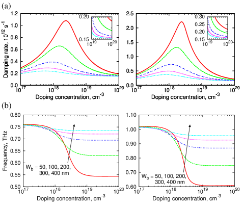
Figures 2(a) and (b) show the dependences of the plasmon damping rate and frequency on the substrate doping concentration with the plasmon wavenumber cm-1 (i.e., the wavelength m) and with different thicknesses of the bottom dielectric layer, . The value of the plasmon wavelength is chosen so that it gives the frequency around THz in the limit . They clearly demonstrate that there is a huge resonant increase in the damping rate at around cm-3 as well as a drop of the frequency. This is the manifestation of the resonant coupling of the graphene plasmon and the substrate surface plasmon. The resonance corresponds to the situation where the frequencies of graphene plasmons and substrate surface plasmons coincide, in other words, where the exponentially decaying tail of electric field of graphene plasmons resonantly excite the substrate surface plasmons.
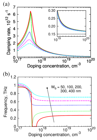
At the resonance, the damping rate becomes larger than s-1, over times larger than the contribution from the acoustic-phonon scattering in graphene, s-1. For structures with and nm, even the damping rate is so large that the frequency is dropped down to zero; this corresponds to an overdamped mode. It is seen in Figs. 2(a) and (b) that the coupling effect becomes weak as the thickness of the bottom dielectric layer increases. The coupling strength at the resonance is determined by the ratio of the electric fields at the graphene layer and at the interface between the bottom dielectric layer and substrate. In the case of the ungated structure with a relatively low doping concentration, it is roughly equal to . Since m is much larger than the thicknesses of the bottom dielectric layer in the structures under consideration, i.e., , the damping rate and frequency in Figs. 2(a) and (b) exhibit the rather slow dependences on the thickness.
Away from the resonance, we have several nontrivial features in the concentration dependence of the damping rate. On the lower side of the doping concentration, the damping rate increase does not vanish until cm-3. This comes from the wider field spread of the channel mode into the substrate due to the ineffective screening by the low-concentration holes. On the higher side, one can also see a rather broad linewidth of the resonance with respect to the doping concentration, owning to the large, concentration-dependent damping rate of the substrate surface plasmons, and a contribution to the damping rate is not negligible even when the doping concentration is increased two-orders-of-magnitude higher. In fact, with cm-3, the damping rate is still twice larger than the contribution from the acoustic-phonon scattering. The inset in Fig. 2(a) indicates that the doping concentration must be at least larger than cm-3 for the coupling effect to be smaller than the contribution from the acoustic-phonon scattering, although the latter is still nonnegligible. It is also seen from the inset that, with very high doping concentration, the damping rate is almost insensitive to . This originates from the screening by the substrate that strongly expands the field spread into the bottom dielectric layer.
As for the dependence of the frequency, it tends to a lower value in the limit than that in the limit , as seen in Figure 2(b), along with the larger dependence on the thickness . This corresponds to the transition of the channel mode from an ungated plasmon mode to a gated plasmon mode, where the substrate effectively acts as a back gate.
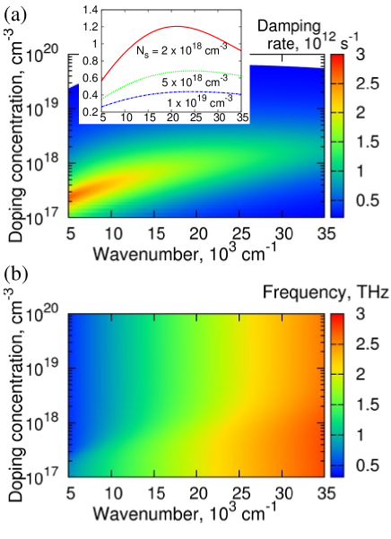
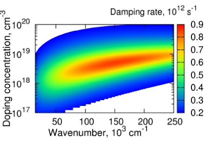
To illustrate the coupling effect with various frequencies in the THz range, dependences of the plasmon damping rate and frequency on the substrate doping concentration and plasmon wavenumber with nm are plotted in Figs. 3(a) and (b). In Fig. 3(a), the peak of the damping rate shifts to the higher doping concentration as the wavenumber increases, whereas its value decreases. The first feature can be understood from the matching condition of the wavenumber-dependent frequency of the ungated graphene plasmons and the doping-concentration-dependent frequency of the substrate surface plasmons, i.e., , roughlly speaking, and . The second feature originates from the exponential decay factor, , of the electric field of the channel mode at the interface between the bottom dielectric layer and the substrate; since the doping concentration is cm-3 at the resonance for any wavevector in Fig. 3, the exponential decay is valid. Also, with a fixed doping concentration, say cm-3, the damping rate has a maximum at a certain wavenumber, resulting from the first feature (see the inset in Fig. 3(a)).
IV Gated Plasmons
Next, we study plasmons in the gated structures. We consider the same electron concentration, ficticious mass, and collision frequency, cm-2, , and s-1, as the previous section. As examples of materials for top/bottom dielectric layers, we examine Al2O3/SiO2 and diamond-like carbon (DLC)/3C-SiC. These materials choices not only reflect the realistic combination of dielectric materials available today, but also demonstrate two distinct situations for the coupling effect under consideration, where for the former and for the latter.
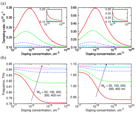
Figures 4(a) and (b) show the dependences of the plasmon damping rate and frequency on the substrate doping concentration with the wavenumber cm-1 (the plasmon wavelength m), with thicknesses of the Al2O3 top dielectric layer and nm, and with different thicknesses of the SiO2 bottom dielectric layer, . As seen, the resonant peaks in the damping rate as well as the frequency drop due to the coupling effect appear, although the peak values are substantially smaller than those in the ungated structure (cf. Fig. 2). The peak value decreases rapidly as the thickness of the bottom dielectric layer increases; it almost vanishes when nm. These reflect the fact that in the gated structure the electric field of the channel mode is confined dominantly in the top dielectric layer due to the gate screening effect. The field only weakly spreads into the bottom dielectric layer, where its characteristic length is roughtly proportional to , rather than the wavelength as in the ungated structure. Thus, the coupling effect on the damping rate together with on the frequency vanishes quickly as increases, even when the wavenumber is small and . More quantitatively, the effect is negligible when the first factor of given in Eq. (8) in the limit and ,
| (11) |
is small, i.e., when the factor is much larger than unity. A rather strong dependence of the damping rate on can be also seen with high doping concentration, in the insets of Fig. (4)(a).
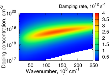
Figure 5 shows the dependence of the plasmon damping rate on the substrate doping concentration and plasmon wavenumber, with dielectric layer thicknesses and nm. As compared with the case of the ungated structure (Fig. 3(a)), the peak of the damping rate exhibits a different wavenumber dependence; it shows a broad maximum at a certain wavenumber (around cm-1 in Fig. 5) unlike the case of the ungated structure, where the resonant peak decreases monotonically as increasing the wavenumber. This can be explained by the screening effect of the substrate against that of the top gate. When the wavenumber is small and the doping concentration corresponding to the resonance is low, the field created by the channel mode is mainly screened by the gate and the field is weakly spread into the bottom direction. As the doping concentration increases (with increase in the wavevector which gives the resonance), the substrate begins to act as a back gate and the field spreads more into the bottom dielectric layer, so that the coupling effect becomes stronger. When the wavenumber becomes so large that does not hold, the field spread is no longer governed dominantly by the substrate or gate screening, i.e., the channel mode begins to be “ungated” by the substrate. Eventually, the coupling effect on the damping rate again becomes weak, with the decay of the field being proportional to .
As illustrated in Eq. (11), the coupling effect in the gated strcture is characterized by the factor when the conditions and are met. This means that not only the thicknesses of the dielectric layers but also their dielectric constants are very important parameters to determine the coupling strength. For example, if we adapt the high-k material, e.g., HfO2 in the top dielectric layer, it results in the more effective gate screening than in the gated structure with the Al2O3 top dielectric layer, so that the coupling effect can be suppressed even with the same layer thicknesses. The structure with the DLC top and 3C-SiC bottom dielectric layers (with 29 and ) corresponds to the quite opposite situation, where the gate screening becomes weak and the substrate screening becomes more effective, so that stronger coupling effect is anticipated. Figures 6(a), (b), and 7 show the same dependences as in Figs 4(a), (b), and 5, respectively, for the structure with the DLC top and 3C-SiC bottom dielectric layers. Comparing with those for the structure with the Al2O3 top and SiO2 bottom dielectric layers, the damping rate as well as the frequency are more influenced by the coupling effect in the entire ranges of the doping concentration and wavevector. In particular, the increase in the damping rate with high doping concentration cm-3 and the thickness of the bottom layer nm, which are typical values in real graphene samples, is much larger. However, this increase can be avoided by adapting thicker bottom layer, say, nm or by increasing the doping concentration.
V Conclusions
In summary, we studied theoretically the coupling of plasmons in graphene at THz frequencies with surface plasmons in a heavily-doped substrate. We demonstrated that in the ungated graphene structure there is a huge resonant increase in the damping rate of the “channel mode” at a certain doping concentration of the substrate ( cm-2) and the increase can be more than s-1, due to the resonant coupling of the graphene plasmon and the substrate surface plasmon. The dependences of the damping rate on the doping concentration, the thickness of the bottom dielectric layer, and the plasmon wavenumber are associated with the field spread of the channel mode into the bottom dielectric layer and into the substrate. We revealed that even with very high doping concentration ( cm-2), away from the resonance, the coupling effect causes nonnegligible increase in the damping rate compared with the acoustic-phonon-limited damping rate. In the gated graphene structure, the coupling effect can be much reduced compared with that in the ungated structure, reflecting the fact that the field is confined dominantly in the top dielectric layer due to the gate screening. However, with very high doping concentration, it was shown that the screening by the substrate effectively spreads the field into the bottom dielectric layer and the increase in the damping rate can be nonnegligible. These results suggest that the structural parameters such as the thicknesses and dielectric constants of the top and bottom dielectric layers must be properly chosen for the THz plasmonic devices in order to reduce the coupling effect.
Acknowledgements.
Authors thank M. Suemitsu and S. Sanbonsuge for providing information about the graphene-on-silicon structure and Y. Takakuwa, M. Yang, H. Hayashi, and T. Eto for providing information about the diamond-like-carbon dielectric layer. This work was supported by JSPS Grant-in-Aid for Young Scientists (B) (#23760300), by JSPS Grant-in-Aid for Specially Promoted Research (#23000008), and by JST-CREST.References
- (1) M. Dyakonov and M. Shur, Phys. Rev. Lett. 71, 2465 (1993).
- (2) M. Dyakonov and M. Shur, IEEE Trans. Electron Devices 43, 380 (1996).
- (3) M. S. Shur and J.-Q. Lü, IEEE Trans. Micro. Th. Tech. 48, 750 (2000).
- (4) M. S. Shur and V. Ryzhii, Int. J. High Speed Electron. Sys. 13, 575 (2003).
- (5) F. Teppe, D. Veksler, A. P. Dmitriev, X. Xie, S. Rumyantsev, W. Knap, and M. S. Shur, Appl. Phys. Lett. 87, 022102 (2005).
- (6) T. Otsuji, Y. M. Meziani, T. Nishimura, T. Suemitsu, W. Knap, E. Sano, T. Asano, V. V. and Popov, J. Phys.: Condens. Matter 20, 384206 (2008).
- (7) V. Ryzhii, A. Satou, M. Ryzhii, T. Otsuji, and M. S. Shur, J. Phys.: Condens. Matter 20, 384207 (2008).
- (8) V. V. Popov, D. V. Fateev, T. Otsuji, Y. M. Meziani, D. Coquillat, and W. Knap, Appl. Phys. Lett. 99, 243504 (2011).
- (9) T. Watanabe, S. Boubanga Tombet, Y. Tanimoto, Y. Wang, H. Minamide, H. Ito, D. Fateev, V. Popov, D. Coquillat, W. Knap, Y. Meziani, and T. Otsuji, Solid-State Electron. 78, 109 (2012).
- (10) V. Ryzhii, Jpn. J. Appl. Phys. 45, L923 (2006); V. Ryzhii, A. Satou, and T. Otsuji, J. Appl. Phys. 101, 024509 (2007).
- (11) T. Otsuji, S. A. Boubanga Tombet, A. Satou, H. Fukidome, M. Suemitsu, E. Sano, V. Popov, M. Ryzhii, and V. Ryzhii, J. Phys. D: Appl. Phys. 45, 303001 (2012).
- (12) A. N. Grigorenko, M. Polini, and K. S. Novoselov, Nat. Photon. 6, 749 (2012).
- (13) E. Hwang and S. Das Sarma, Phys. Rev. B 77, 115449 (2008).
- (14) V. Ryzhii, T. Otsuji, M. Ryzhii, and M. S. Shur, J. Phys. D: Appl. Phys. 45, 302001 (2012).
- (15) V. Ryzhii, M. Ryzhii, and T. Otsuji, J. Appl. Phys. 101, 083114 (2007).
- (16) M. Ryzhii and V. Ryzhii, Jpn. J. Appl. Phys. 46, L151 (2007).
- (17) A. A. Dubinov, V. Ya Aleshkin, V. Mitin, T. Otsuji, and V. Ryzhii, J. Phys.: Condens. Matter 23, 145302 (2011).
- (18) V. Popov, O. Polischuk, A. Davoyan, V. Ryzhii, T. Otsuji, and M. Shur, Phys. Rev. B 86, 195437 (2012).
- (19) Y. Takatsuka, K. Takahagi, E. Sano, V. Ryzhii, and T. Otsuji, J. Appl. Phys. 112, 033103 (2012).
- (20) L. Ju, B. Geng, J. Horng, C. Girit, M. Martin, Z. Hao, H. Bechtel, X. Liang, A. Zettl, Y. R. Shen, and F. Wang, Nat. Nanotechnol. 6, 630 (2011).
- (21) J. H. Strait, P. Nene, W.-M. Chan, C. Manolatou, S. Tiwari, F. Rana, J. W. Kevek, and P. L. Mceuen, Phys. Rev. B 87, 241410 (2013).
- (22) M. Suemitsu, Y. Miyamoto, H. Handa, and A. Konno, e-J. Surf. Sci. Nanotech. 7, 311 (2009).
- (23) N. Horing, Phys. Rev. B 80, 193401 (2009).
- (24) J. Yan, K. Thygesen, and K. Jacobsen, Phys. Rev. Lett. 106, 146803 (2011).
- (25) A. Satou, V. Vyurkov, and I. Khmyrova, Jpn. J. Appl. Phys. 43, 566 (2004).
- (26) D. Svintsov, V. Vyurkov, S. Yurchenko, T.Otsuji, and V. Ryzhii, J. Appl. Phys. 111, 083715 (2012).
- (27) C. Bulucea, Solid-State Electron. 36, 489 (1993).
- (28) S. A. Maier, Plasmonics: Fundamentals and Applications (Springer Science, NY, 2007).
- (29) The dielectric constant of DLC varies in the range between and , depending on its growth condition 30. Here, we choose the lowest value for demonstration of the case where .
- (30) H. Hayashi, S. Takabayashi, M. Yang, R. Ješko, S. Ogawa, T. Otsuji, and Y. Takakuwa, “Tuning of the dielectric constant of diamond-like carbon films synthesized by photoemission-assisted plasma-enhanced CVD,” in 2013 International Workshop on Dielectric Thin Films for Future Electron Devices -Science and Technology- (2013 IWDTF), Tokyo, Japan, November 7-9, 2013.