Charge Pumping Through a Single Donor Atom
Abstract
Presented in this paper is a proof-of-concept for a new approach to single electron pumping based on a Single Atom Transistor (SAT). By charge pumping electrons through an isolated dopant atom in silicon, precise currents of up to 160 pA at 1 GHz are generated, even if operating at 4.2 K, with no magnetic field applied, and only when one barrier is addressed by sinusoidal voltage cycles.
1 Introduction
Although some fascinating alternatives have been recently suggested, e.g. semiconductor quantized voltage sources see Ref. Hoh056802 , the main task of the electrical branch of quantum metrology remains the development of reliable quantised electron pumps (QEPs) Mil279 ; Gib1 ; Pot249 ; Kou1626 ; Kel1804 ; Blu343 ; Pek120 ; Jeh021012 ; Fuj042102 ; Kae012106 ; Sie3841 and, as a consequence, the full implementation of the quantum metrology triangle Mil279 . The QEP approach to metrology was introduced in the early 90s Pot249 and, since then, many interesting schemes have been proposed, each with advantages and disadvantages – see Ref. Gib1 ; Pot249 ; Kel1804 ; Blu343 ; Pek120 ; Fuj042102 ; Kae012106 ; Sie3841 . The strong focus on QEP-based metrology is also justified by its ability to generate currents in which capture and emission processes can be controlled at the single electron level. This can be obtained by taking advantage of Coulomb Blockade (CB) effects Bee1646 as QEPs are often Single Electron Transistor (SET) based Gib1 ; Pot249 ; Kel1804 ; Blu343 ; Pek120 ; Fuj042102 ; Kae012106 ; Sie3841 .
To be useful for metrology, a QEP needs to generate currents of the order of hundreds of with accuracies of 1 part in (equivalent to ppm). Furthermore, as the current () is linked to the frequency of oscillation () according to the simple relation Pot249 , with being the elementary charge, GHz is necessary to generate the desired currents. At GHz frequencies, QEPs are known to be affected by non-adiabatic excitation errors Kat126801 ; Kas186805 . It is already understood that, to improve robustness and, as a consequence, temperature and speed of operations, their charging energy () needs to be increased FleR16291 . The is the energy that needs to be paid to a system to increase the average number of electrons it contains by one Pot249 ; Blu343 and, for Quantum Dots (QDs), is inversely proportional to its size, which makes increasing it in conventional QD-SETs is a non-trivial task Shi103101 . Between the many approaches available, the one that has proven to be both successful and reproducible is based on single atom transistors (SATs) Sel206805 ; Roc206812 ; Mor345 ; Fue242 ; Pla541 ; Tet046803 .
High currents and high accuracies have been recently achieved Gib1 in a single-parameter charge pumping configuration Fuj042102 ; Kae012106 similar to the one used in this work and every possible novelty in the technology used to fabricate and to operate a QEP represents an important milestone Mil279 ; Hoh056802 . As this article will show, an isolated shallow dopant atom, due to the combination of a high and a well isolated ground state for the first electron charge state, provides, naturally, an interesting geometry for the quantum pumping of electrons. This is not the first time that dopant atoms have been used to generate pumping currents. Lansbergen et al Lan763 and more recently Roche et al Roc1581 used a few dopants FET to perform pumping at MHz frequency, however, these pioneering experiments were not at the single atom level and far from the rates requested for quantum metrology.
After a short introduction of the devices structure, of the selection process for the location of the good devices amongst the large pool of fabricated ones and of the experimental setup in section 2, in section 3 we discuss the generation of pumped current up to the GHz frequencies and we show that, for our system, it is possible to reach the = fe quantisation even for = 1 GHz. Some considerations on the consequences of our results are discussed in section 4. In the appendix (section A.1) we give more insight on the differences between the non-adiabatic regime (studied in our experiment) and the adiabatic pumping regime. Lastly, more details on some aspects of our experiments are discussed in the appendix (sections A.2, A.3 and A.4).
2 Devices selection and measurement setup
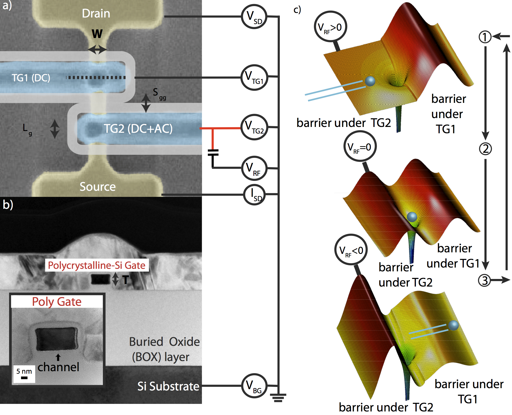
The devices used in our experiments are fabricated on a Complementary-Metal-Oxide-Semiconductor (CMOS) platform Roc206812 ; Roc032107 ; Wac193 making them fully compatible with one of the most successful technologies of modern times. An adapted Roc032107 fully depleted-silicon on insulator (FD-SOI) technology (see Fig. 1) is used to fabricate n-metal-oxide-semiconductor field-effect-transistors (n-MOSFET’s). The 20 nm thick SOI channel is initially doped with a background concentration of and then is etched to form the channel of the device which is sitting on top of a 150 nm thick buried oxide (BOX), as shown in Fig. 1b). The device fabrication is then completed by using a technology similar to that used in commercial trigate SOI MOSFETs Roc032107 . The only difference is that, in our devices, not only one gate (polycrystalline silicon) is wrapped around three sides of the channel (see Fig. 1b)), but two are positioned in series (see Fig. 1a)) along the direction of electron transport. Finally, to protect the channel from the high doping doses (HDDs) necessary for the formation of the source and the drain regions, 15 nm thick spacers (see Fig. 1a)) are formed around the two gates Roc206812 and the HDDs implantation is performed at an angle of 55 degrees. This configuration prohibits dopants from the HDD from reaching the portion of the channel between the two gates. Furthermore, within this channel, the original doping yields only a few active atoms, which provide the states shown in Fig. 3, hence allowing the observation of the SAT behaviour Sel206805 ; Roc206812 ; Mor345 ; Fue242 ; Pla541 ; Tet046803 . Note that in our devices the atoms are present in the centre of the channel only due to the initial background doping procedure discussed above. Furthermore, as shown in Fig. 2a) and Fig. 3, room and low temperature Wac193 ; Roc206812 electrical characterisation can be used to study the presence of this discrete number of isolated dopants in the channel and their effects on the transport characteristics.
The low temperature measurements were performed by mounting the device on a stage that is dipped directly in liquid helium and thus at 4.2 K. A low noise battery operated measurement setup (see Ref. Van4394 ; Vin123512 ; Koppens ) was used to measure the source/drain current and to apply the voltages. As the amplifier is at room temperature, the absolute noise floor of the IV-converter is limited by the Johnson noise of the feedback resistor, which is given by = 4 . To apply the sinusoidal RF input to one gate an Agilent 8648C source was used. An important aspect of our setup is that a cryogenic bias-T Gib1 , in red in the circuit schematic of Fig. 1a) and 1b), is used to add this RF voltage to one of the two DC voltages applied to both the gates; this in a single-parameter charge pumping configuration Gib1 ; Fuj042102 ; Kae012106 .
Our double gate (TG1 and TG2 in Fig. 1a)) configuration allows the control of both the left and the right barriers, thereby confining the electrons into the atomic potential using an approach similar to the one recently implemented elsewhere Gib1 ; Blu343 ; Fuj042102 ; Kae012106 . However, differently from previous ones Gib1 ; Blu343 ; Kae012106 , in our approach each gate is capacitively coupled with the dopant state (in a way similar to that of the global top gate used in ref. Fuj042102 or of the back gate in ref. Sie3841 ) and, to some extent, can also cross-couple to the barrier under the opposite gate, e.g. see schematic in Fig. 2b) and Fig. 4b). This makes it possible to observe a pumping behaviour not previously observed in conventional pumps. As an example, in our devices the distinction between ”entrance” and ”exit” gates is not as sharp as in conventional QEPs Gib1 ; Kae012106 , which explains why both the gates can be used for the evaluation of the quantisation (pumping) effects.
Two QEPs, i.e. devices and , structurally similar to the one shown in Fig. 1a) and Fig. 1b) and having channel widths (s) equal 60 nm and 800 nm and gates lengths (s) equal 50 nm and 20 nm, respectively, have been selected between the many available and studied at 4.2 K.
Initially, many devices are measured at room temperature. Source-drain current versus TG1 (TG2) traces are acquired by keeping the other gate, TG2 (TG1), grounded as shown in Fig. 2. The following signatures (e.g. see Fig. 2) are used to select the good devices amongst the large pool of fabricated ones Roc206812 ; Wac193 :
-
1.
Negative threshold voltages, 0 mV, indicating the dominance by a discrete number of dopant atoms in the sub-threshold region of transport Wac193 .
-
2.
Almost symmetric behaviour of the gates (indicating a good control of the channel by both the gates) and good results in the lithography of the poly-gates themselves.
-
3.
The capability that each gate has, independently from the other, to control the channel (and to turn the transistor to the ON-state). This, at low temperature, results in the important feature that each gate can, to some extend, have some cross-coupling with the barrier under the opposite gate (as schematically shown in Fig. 2b)).
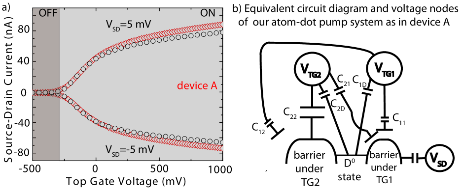
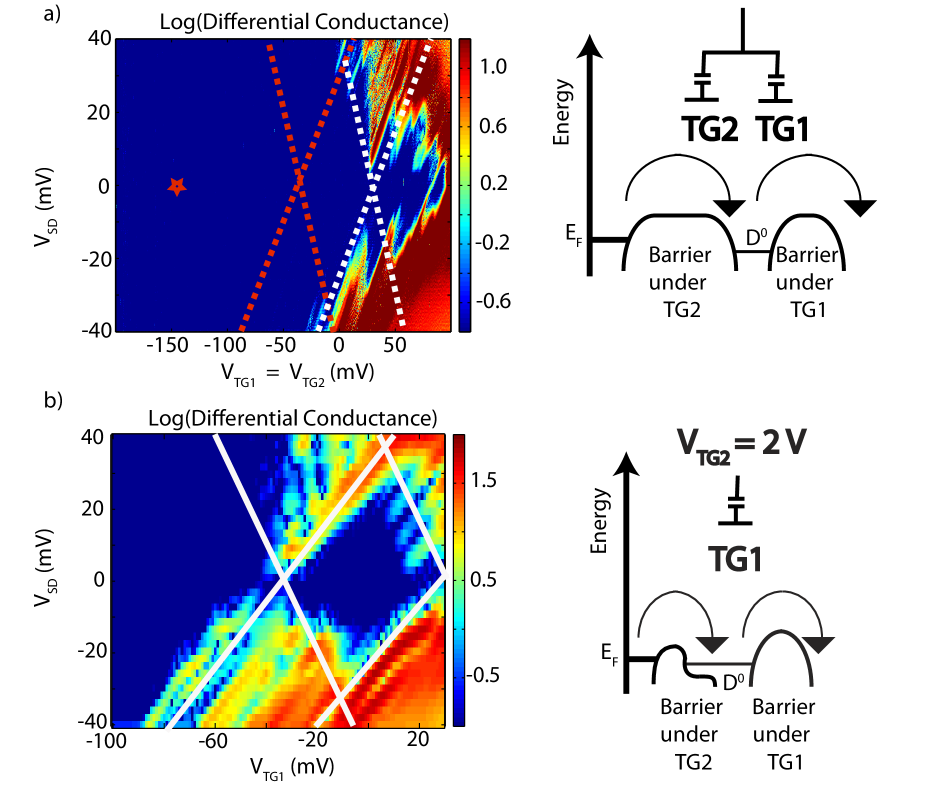
The data in Fig. 2a) are related to the room temperature characterisation of device studied in the main part of the manuscript, a similar selection process has been followed for device . The data in Fig. 3 are related to 4.2 K characterisation of device . For devices having the distance between the two top gates () = 50 nm, such as device and device , only for and 100 mV can artificial atom systems (i.e. QDs) be induced under the two top gates. Therefore, the sub-threshold (for and 100 mV) current signature can only be dopant related, see also similar results in Ref. Roc206812 ; Wac193 ; Lan763 ; Roc1581 . Fig. 3 indicates that our approach enables the few electrons regime Roc206812 to be accessed and gives a first indication of the fact that, for device , the first charge state () of a single isolated dopant atom (located in the central region of the channel) is addressed. As our pumping approach requires low transparency of the tunnel barriers, the exact quantification of the in the CB diamonds of Fig. 3a) is not straightforward. The estimation of 35 meV obtained in this Fig. 3a), however, was confirmed in the strong coupling regime Tet046803 measurements of Fig. 3b). This strong coupling regime is not optimal for pumping but it allows the observation of the CB diamond for a gate position similar to the one where it is only partially visible in Fig. 3a).
These results agree with the analysis of the AC data discussed in section 3 and with recent observations by other groups Roc206812 ; Wac193 ; Lan763 ; Roc1581 . Furthermore, for our pumping experiments, the channel thickness () and have always been fixed at 20 nm and 50 nm respectively because, unlike and , the parameter has proven to be important. As an example, the absence of transport in the sub-threshold region and a regular double quantum dot (DQD) signature Wie1 in the region of inversion, i.e. for ’s 100 mV, have been observed for other measured devices having 50 nm (see section A.2). These facts are an indication of the absence of transport through isolated dopants and indeed pumping through isolated dopants has proved not to be possible in this latter case.
3 Radio frequency (RF) measurements
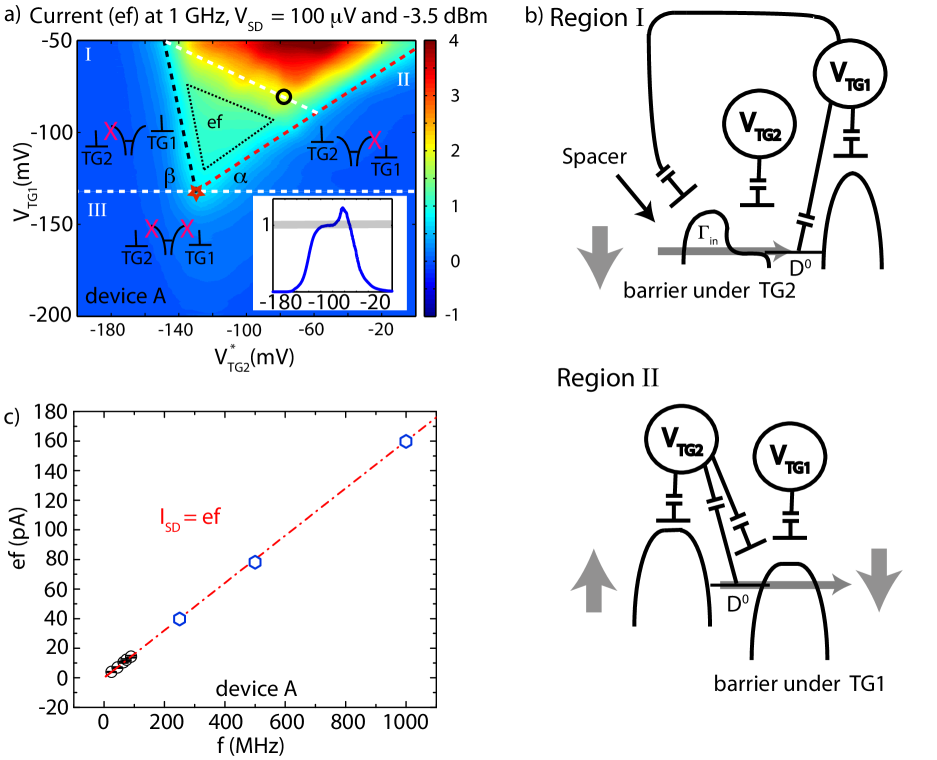
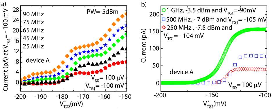
We can now turn to the radio frequency (RF) measurements of device . In Fig. 4, Fig. 5, Fig. 6 and Fig. 7, the data related to the generation of pumping currents when a sinusoidal voltage excitation, , is provided to TG2 are shown. The asterisk, ””, used for the AC data, indicates for each pump which of two gates is excited by RF oscillations. Taking advantage of the knowledge gained in the DC transport experiments illustrated in Fig. 3, the top gates are tuned to values far from the ones of the DC transport regime, i.e. in the region indicated with the red star in Fig. 3a). For these voltage values, transport can only be related to the transiting of electrons through the atom-dot following the pumping scheme introduced in Fig. 1c). This is also illustrated in Fig. 4c), where the reaching of unity steps proportional to the frequencies of excitation, , ranging from 25 MHz to 1 GHz and the subsequent following of the expected = law are shown. Furthermore, in our pumps, the sign of the current does not depend on the sign of but on which gate is selected to be RF excited Fuj042102 ; Fle155311 , i.e. the data of Fig. 8 related to device have been acquired by using = - 2 mV. The independence of the current from the source/drain polarity is another strong indication of the pumping nature of a current Fuj042102 . These last facts allow us to illustrate some of the great advantages of our SAT based single-parameter configuration, which, by combining an isolated ground state with large ’s, allows the extension of the non-adiabatic pumping regime Kae012106 ; Fuj042102 ; Kae153301 for at least three orders of magnitude, i.e. from the MHz to the GHz regime of operations. This also occurs since a careful control of the phase of the excitation is not necessary Fuj042102 .
As shown below, the analysis of the triangular shape observed in Fig. 4a) (and in Fig. 5 and Fig. 6) brings further evidence that the pumping signature studied for device is dopant related. In region III, the AC transport is never possible. In region I, opposite to angle , the current is limited because the electrons are blocked at the entrance of the pump (stage 1 in Fig. 1c)). This is true unless TG1 can compensate for the lack of action of TG2 in addressing the barrier under it and the state Lei911 . This also justifies the association between and the value of coupling between TG1 and the state and the value of the cross-coupling between TG1 and the barrier under TG2, see Fig. 4b) for a schematic. The estimated value for (the voltage ratio = is 8.5, hence 83.3 degrees) indicates that the black dotted onset line is 6.7 degrees more tilted in the anti-clockwork direction compared to the case of having the state coupled only to TG2 and no cross-coupling between TG1 and the barrier under TG2, i.e. this case should lead to = 90 degrees Lei911 . To clarify this aspect we can see if the observed dependence of to agrees with it. It should be noted that expected can be extrapolated, and so as to observe full quantisation, the entrance rate ( in Fig. 4b)) in the first half of the cycle must be large compared to Lei911 . So if the value of increases, is expected to increase, i.e.: it becomes more difficult for TG1 to be effective in correcting the lack of action of TG2 in lowering the barrier. This occurrence is demonstrated in Fig. 5, where it is demonstrate that the angle increases following an increase of . Indeed, being = 6.5 and = 8.5, we have = 81.2 degrees and = 83.3 degrees.
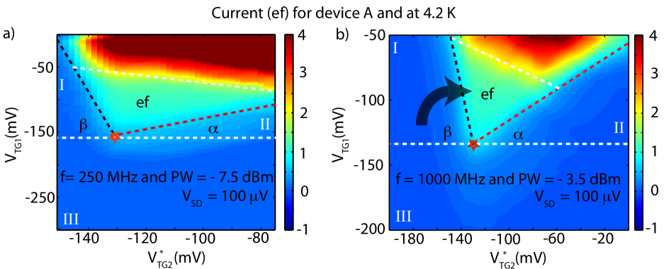
In region II, opposite to angle , the pumping current is limited when the electrons are blocked at the exit of the pump (stage 3 in Fig. 1c)). This happens because during each cycle the barrier under TG2 is so low that TG1 needs to be larger than previously to let the electrons leave the atom to the drain, see Fig. 4b). When the DC value of decreases, the exit of the electrons and the complete cycle are facilitated and becomes possible for lower values of . This justifies the association between and the value of the coupling present between TG2 and the state and the value of the cross-coupling between TG2 and the barrier under TG1. The value for (the voltage ratio = is 1.69, hence is 31 degrees) is non-zero. and can only provide an insight into the complicated coupling and cross-coupling effects present in our system (see Fig. 2b)), however, there is an important information that can be extracted from these: the two voltage ratios associated with and are of the same order of magnitude and hence the position of the state can be inferred somewhere at the centre of the channel.
Lastly, the strong frequency dependence of the angles and observed in Fig. 5 could be also related to the capacitive coupling between the gates, as schematically shown in Fig. 2b). This because, during the RF measurements, the ”fixed” gate will oscillate due to stray coupling with the driven gate and the amplitude and the phase of this parasitic oscillation will be frequency dependent.
By following the black and the red dashed lines towards more negative values of it is possible to observe that they do cross (the red star in Fig. 4a) and in Fig. 5). In conventional electron pumps Gib1 ; Kae012106 ; Fle155311 ; Lei911 , the confinement site is created by applying negatively voltages above a two-dimensional electron gas (2-DEG) and the energy state of the QD is completely manipulated by the barriers and crosses the Fermi level when the barriers are already transparent enough to observe pumping current Lei911 . Moreover, the state used for pumping is localised in a region that comprises many atomic sites and as a consequence, for these 2-DEG induced QDs Gib1 ; Kae012106 ; Lei911 , there is always a certain range of and where the onset of the pumping transport can be observed (i.e. the shape of the plateau in the 2D stability is trapezoidal and not triangular). This observation reflects the fact that for these confining potentials the states are not strongly localised and can tolerate some deformation from the gates before transiting from one regime to another. However, when the localisation of the state is increased, for example following the application of a magnetic field perpendicular to the plane Gib1 ; Kae012106 ; Fle155311 , a drastic reduction of this range of tolerance, is observed. Indeed, as shown in Fig. 2 of ref Kae012106 , the trapezoidal shape of the 2D stability approaches the triangular one with the application of a magnetic field.
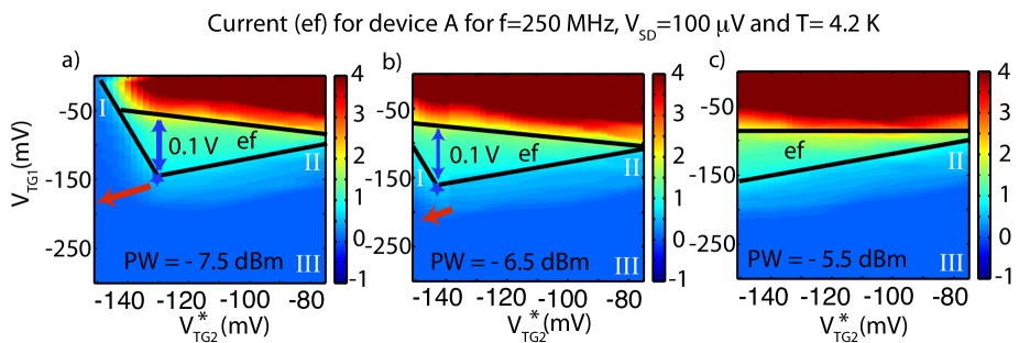
The fact that in our system this region of tolerance is reduced to a small region of the 2D stability (red star in in Fig. 4a) and in Fig. 5), even without the presence of a magnetic field, indicates that the potential confining the electrons is localised in a few atomic sites, i.e. is related to an isolated donor atom Sel206805 and not a QD. This occurs because, for an atom pump, the barriers are not transparent enough when the state crosses the Fermi level (as also seen in Fig. 3a)) and the crossing line is only seen for the second electron (outlined by the black circle in Fig. 4a)). Furthermore, as shown in the Fig. 6 for = 250 MHz, following an increase of the RF power (PW) from -7.5 dBm to -5.5 dBm, the triangular shape equivalent to the one observed in 4a) does not seems to be dramatically deformed but just shifted towards more negative gate voltage values. This last observation is dramatically different from the ones attributed to conventional QEPs, see ref Gib1 ; Kae012106 ; Lei911 and references therein. This is again in agreement with the idea that a strong local potential, having a shape less affected by the gates if compared to conventional QEPs, is responsible for the confinement of our pumping electrons, making that the increase of PW can move the onset of the pumping current to more negative of the DC gate voltages. Lastly, the second plateau observed in Fig. 4a) (black circle) can be associated with the state ( state Lan136602 ) of the first atom or with the state of a second atom. For this reason, in this paper, we only study the first quantisation step.
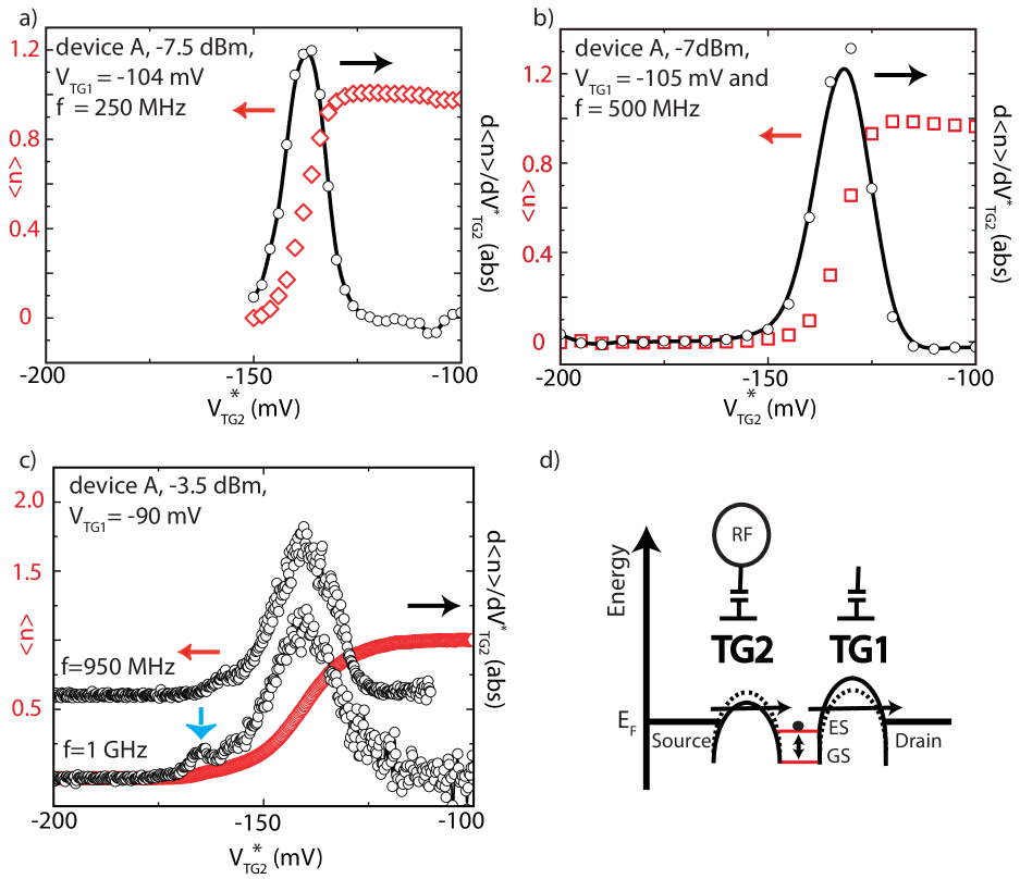
To conclude the discussion on device , Fig. 7 shows the data for the RF currents and the derivative of the currents for different frequencies. From the data of Fig. 7 it is possible to extrapolate that, in our system, the onset of the pumping current starts to be mildly affected by non-adiabatic excitations Kat126801 ; Fle155311 only for 1 GHz and, as also shown in Fig. 4, little degradation of the quantisation is observed even for this range of frequencies. If we compare this to the onset of non-adiabatic excitations observed in QD-QEPs Kat126801 ; Fle155311 , i.e. 200 MHz, we have another indication of the fact that the system addressed in our experiments is characterised by higher energies if compared to conventional QEPs. Indeed, for a SAT Roc206812 , all the energy scales (e.g. 30-40 meV and = - 10 meV, with being the ground state and the first excited state) are higher if compared to the ones of a QD-QEP Kat126801 ; Fle155311 and it is therefore possible to observe charge pump quantisation at 1 GHz. Plus, even if our SAT pumps are operating at relatively high temperatures ( 4.2 K), as the condition 0 is still holding, thermal errors Zim5254 can be ignored. In conclusion, in our SAT system, high (i.e. immunity to thermal effects) combined with the isolated ground state (i.e. immunity to non-adiabatic excitations) allows the observation of the quantised non-adiabatic regime Kae153301 for a wide range of frequencies. This is telling us that the use of SAT systems Sel206805 ; Roc206812 ; Fue242 having larger and larger signatures, if compared to the ones associated to the present system, could allow further improvements of the pumping performances.
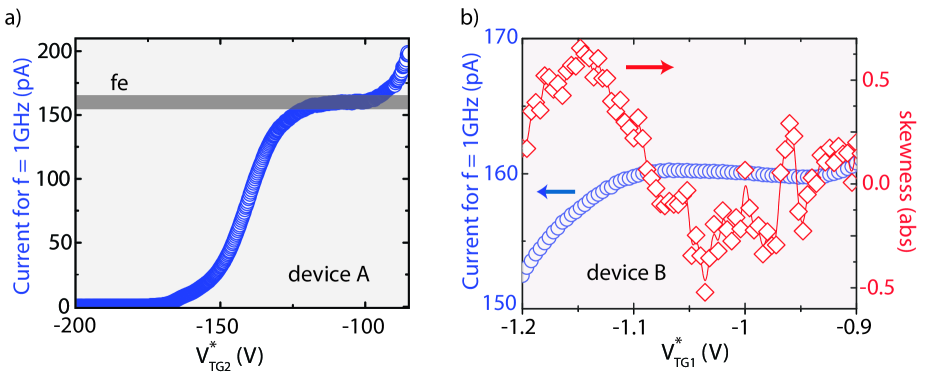
From the data of device , selected and characterised via room and low temperature DC measurements identical to device , we gain a more precise idea of the robustness of our SAT approach. As the setup used in our experiments is a state-of-the-art custom build ultra low noise apparatus Van4394 ; Vin123512 ; Koppens ; it is able to provide a noise floor of when a 1 G feedback resistor is used in the amplification and when a 0.1 G feedback resistor is used (as for all our data). Hence, in this configuration, a 10 Hz bandwidth will lead to the association of 40 of error to each point. Furthermore, the current data of this Fig. 8b) has been obtained by repeating the same 10 Hz bandwidth trace 1200 times in 24 and therefore the effective bandwidth could be as low as . However, the optimal bandwidth was estimated by also taking into account the long time instabilities associated with our room temperature acquisition system. In the case of the current data of Fig. 8 b), the optimal trade-off leads to a bandwidth around 1.6 Hz and to an estimated error of around 15 fA for each point in the plateau. Indeed, a standard error of the mean of this order of magnitude has been also extracted from the data in the plateau region of this Fig. 8b). These facts give an indication on the robustness and on the reproducibility that can be associated to our system. Furthermore, the data of Fig. 8 are important as they demonstrated that we can obtain the = quantisation for = 1 GHz in two different devices.
4 Conclusions
The results presented in this paper link pumping of electrons in a single-parameter configuration to the first charge state of a single isolated atomic potential. Although the SAT approach to QEP shows some differences from the ones based on conventional pumps, as an atom provides an isolated ground state with high charging energy, this system appears to be a promising QEP geometry. The fact that the quantisation can be observed in two different devices, even when the gate oscillates at 1 GHz, is of interest as it was obtained at 4.2 K, without the need for a high magnetic field to increase confinement and specifically designed cycles to avoid dramatic non-adiabatic excitations. Furthermore, this result aligns with requests by the most recent theoretical proposals Wul1 and indicates that the atom potential provides naturally a good charge pumping system.
In our work, we not only demonstrated the single atom limit of pumping in a CMOS compatible device, but also the validity of earlier theoretical predictions Blu343 ; FleR16291 linking high ’s with high of operations. The simplicity of our approach, requiring only liquid helium temperatures, should allow easy scaling to the more complicated devices recently suggested for error correction Wul1 . As there is a large research effort in the direction of the fabrication of SATs Sel206805 ; Roc206812 ; Fue242 ; Pla541 , progress could be rapid. In conclusion, this work demonstrates that an isolated dopant atom is not only a promising platform to build a quantum computer Pla541 , but also for QEPs.
Acknowledgments
The devices used in this work have been designed and fabricated in the AFSiD Project, see http://www.afsid.eu. The authors thanks K. Beckmann for his help during the initial phases of the experiments and A. Rossi, M. Governale and L. C. L. Hollenberg for some useful discussions during the preparation of this manuscript. G. C. Tettamanzi acknowledges financial support from the ARC-Discovery Early Career Research Award (ARC-DECRA) scheme, project title : Single Atom Based Quantum Metrology and ID: DE120100702 and from the UNSW under the GOLDSTAR Award 2013 scheme. SR acknowledges the ARC FT scheme, project ID: FT100100589.
Appendix
A.1 On the non-adiabatic pumping regime of our RF data
The RF measurements in the main manuscript are all in the quantum non adiabatic pumping regime, as the time scales (frequencies) driving our system are always () than the time scales (frequencies) associated to the dwelling of the electrons into the state. In our system the dwelling times can be extracted via the two tunnelling times of the electrons from or to the leads (i.e. via the slowest of the two). Furthermore, the DC barrier transparencies can be estimated to be more than 1600 ns (less that 625 KHz) for device and around 400 ns for device . Interestingly, for device , the range of the time scales (frequencies) used for the driving RF signal sits between 1 ns (1 GHz) and 40 ns (25 MHz) and therefore always () than 1600 ns (625 KHz). For device B, the system is driven at a time scale (frequency) of 1 ns (1 GHz) which certainly is () than 400 ns (2.5 MHz). The tunnelling times can be extracted from the DC currents observed in the linear (low bias) regime in the following way: for device these currents can be estimated 100 as, in the low bias regime, no signal can be distinguished from the noise back ground of the measurements in Fig. 3 of the section 2, up to 70 mV. Note that, in the AC experiments of device , we are using an amplitude of around 0.1 V for the RF excitation and DC voltages ranging between - 0.2 V and - 0.05 V for the top gates. So we are always in the range between - 0.3 V and 0.05 V during these pumping experiments. For device , the state used for pumping shows only small levels of current ( 400 fA) in the DC condition similar to the one used for pumping. 100 (400) fA represents 0.6 (2.5 ) electrons/s, and a barrier transparency on the order of s ( s), hence these are in the 1.6 (0.4) s = 1600 (400) ns range, justifying our initial assumptions. However, note that there are some substantial differences between the non-adiabatic pumping limit observed in our system and the one discussed in the recent paper by Roche and co-authors Roc1581 , as in this recent work another important time scale, not available for our system, has to be taken into account: i.e. the coupling or interaction between two atomic states. This because, in this recent paper also the non-adiabatic crossing of two different atomic levels is studied. Indeed, this previous work focusses in the adiabatic regime of transport for the study and characterisation (for example via Landau-Zener physics) of a two atoms system and the results that it describes are, of course, of great relevance for the field of quantum electronics based on dopants, but certainly different from the results presented in our manuscript. On another hand, also note that the extrapolations done for our system are in line with the theoretical predictions of Zimmermann et al Zim5254 and of Kaestner et al Kae153301 stating that, in the single parameter pumping regime situation similar to the one we are using, current will always be blocked if one of the tunnelling couplings between dot and the leads does not satisfy the condition to be ”less than a characteristic scale of ” (with being the plank constant and the frequency). As in our experiment with device quantised pumping currents are still observable at 25 , we can, again, indirectly, extrapolate tunnel couplings MHz’s ( 40 ns), therefore giving another strong indication of the fact that, in our AC measurements, we are always in the non-adiabatic pumping regime. Lastly, it is also important to note that, the observation of non-adiabatic quantised charge pumping plateaus up to 1 GHz at 4.2 K and without the use of complex non sinusoidal excitation, would be very difficult to be linked to an object such as a trap or a disordered QD, as none of them could have the sufficiently high charging energy ( 30 meV) and the sufficiently isolated ground state, together.
A.2 More details on the devices selection process
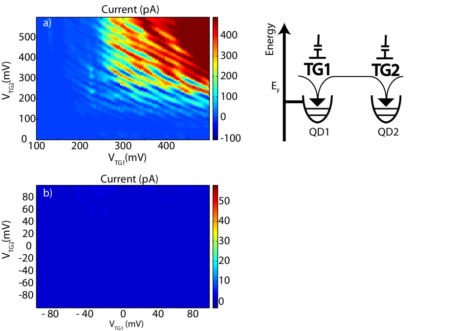
In fact, as the data in Fig. 9 shows, the 2D current diagram for a device very similar to devices and but having 70 nm, e.g. larger than 50 nm, the DQD signature is present while the dopant-atoms signature, especially in the sub-threshold regions of transport, is substantially suppressed. Indeed, in this Fig. 9b), the complete lack of transport for , 100 mV is observed even when (not shown in the Fig. 9) a large source/drain bias is applied. Furthermore, the absence of dopant related signature is also observable in the , 100 mV region of Fig. 9a), i.e. in the DQD region related to the two top gates, as a regular honey-comb structure Wie1 is observed.
Lastly, if the states observed for , 100 mV in Fig. 3 of the main manuscript were related to a QD formed in the centre of the channel and not to dopants, a change of of 20 nm could (slightly) influence their charging energy but would not be sufficient to shift their position of 0.2 V. These facts are an indication of the absence of transport through isolated dopants and indeed pumping through isolated dopants has proved to not be possible in this latter case.
A.3 Current plateaus at different frequencies
In Fig. 10 the evolution of the pumping currents for device and for the different are shown.
A.4 More details on the analysis used for device
Device was used for more accurate tests of the precision of the pumping currents in our system. To tune the barriers under the two top gates, a fixed back gate (BG) voltage value of 5.715 V was found to be an optimal value. However, due to the application of this BG, a small leakage current of a few pA’s was measured both at 1 GHz and at 0 Hz. This leakage is exponential in gate voltage but fully independent of AC excitation. This small current was uniformly subtracted from the original data. Another consequence of the application of the back gate is that slow (few in several hours) two level charge fluctuations lead to a bi-stability of the current. As a consequence of this a different average strategy had to be implemented for this device. During 28 hours a trace was taken approximatively every 72 s and only all the traces that were unaffected by the slow charge trap were included in the average.
References
References
- (1) Hohls, F. et al., Phys. Rev. Lett. 2012, 109, 056802.
- (2) Milton J. T. and Williams, J. M. and Forbes, A. B., Metrologia 2010, 47, 279 and references therein.
- (3) Giblin, S. P. et al., Nature Comm. 2012,3, 1935.
- (4) Pothier, H. et al., Europhys. Lett. 1992, 17, 249.
- (5) Kouwenhoven, L. P. et al., Phys. Rev. Lett. 1991, 67, 1626.
- (6) Keller, M. K. and Martinis, J. M. and Zimmerman, N. M. and Steinbach, A. H., Appl. Phys. Lett. 1996, 69, 1804 (1996).
- (7) Blumenthal, M. D. et al., Nature Phys. 2007, 3, 343.
- (8) Pekola, J. P. et al., Nature Phys. 2008, 4, 120.
- (9) Jehl, X. et al., Phys. Rev. X 2013, 3, 021012.
- (10) Fujiwara, A. and Nishiguchi, K. and Ono, Y., Appl. Phys. Lett. 2008, 92, 042102.
- (11) Kaestner, B. et al., Appl. Phys. Lett. 2009, 94, 012106.
- (12) Siegle, V. et al., Nano Letters 2010, 10, 3841.
- (13) Beenakker, C W. J., Phys. Rev. B 1991, 44, 1646.
- (14) Kataoka, M. et al., Phys. Rev. Lett. 2011, 106, 126801.
- (15) Kashcheyevs, K. and Kaestner, B., Phys. Rev. Lett. 2011, 104, 186805.
- (16) Flensberg, K. and Niu, Q. and Pustilnik, M., Phys. Rev. B 1999, 60, R16291.
- (17) Shin, S. J. et al., Appl. Phys. Lett. 2010, 97, 103101.
- (18) Koenraad, P. M. and Flatte, M.E., Nature Materials 2011, 10, 91.
- (19) Roche, B. et al., Phys. Rev. Lett. 2012, 108, 206812.
- (20) Morton, J. J. L. and McCamey, D. R. and Eriksson, M. A. and Lyon, S.A., Nature 2011, 479, 345.
- (21) Fuechsle, M. et al., Nature Nanotech. 2012, 7, 242.
- (22) Pla, J. P. et al., Nature 2012, 489, 541.
- (23) Tettamanzi, G. C. et al., Phys. Rev. Lett. 2012, 108, 046803.
- (24) Lansbergen, G. P. and Ono, Y. and Fujiwara, A., Nano Letters 2012, 12, 763.
- (25) Roche, B. et al., Nature Comm. 2013, 4, 1581.
- (26) Roche, B. et al., Appl. Phys. Lett. 2012, 100, 032107.
- (27) Wacquez, R. et al., VLSI Technology (VLSIT), 2010 Symposium on , 2010, 193.
- (28) Vandersypen, L. M. K. et al., Appl. Phys. Lett. 2004, 85, 4394.
- (29) Vink, I. T. et al., Appl. Phys. Lett. 2007, 91, 123512.
- (30) Koppens, F. H. L., Coherence and control of a single electron spin in a quantum dot 2007, Casimir PhD Series, Delft-Leiden, 2007-13, ISBN: 978-90-8593-037-2.
- (31) van der Wiel, W. G. et al., Rev. Mod. Phys. , 2002 , 75, 1.
- (32) Fletcher, J. D. et al., Phys. Rev. B , 2012 , 86, 155311.
- (33) Kaestner, B. et al., Phys. Rev. B 2008, 77, 153301.
- (34) Leicht, C. et al., Physica E 2010, 42, 911.
- (35) Lansbergen, G. P. et al., Phys. Rev. Lett. , 2011 , 107,136602.
- (36) Zimmerman, N. M. and Hourdakis, E. and Ono, Y. and Fujiwara, A. and Takahashi, Y., J. Appl. Phys. , 2004 , 96, 5254.
- (37) Wulf, M., Phys. Rev. B 2013, 87, 035312.