Wiedemann-Franz Relation and Thermal-transistor Effect in Suspended Graphene
Abstract
We extract experimentally the electronic thermal conductivity, , in suspended graphene which we dope using a back-gate electrode. We make use of two-point dc electron transport at low bias voltages and intermediate temperatures (50 - 160 K), where the electron and lattice temperatures are decoupled. The thermal conductivity is proportional to the charge conductivity times the temperature, confirming that the Wiedemann-Franz relation is obeyed in suspended graphene. We extract an estimate of the Lorenz coefficient as 1.1 to 1.7 W K-2. shows a transistor effect and can be tuned with the back-gate by more than a factor of 2 as the charge carrier density ranges from 0.5 to 1.8 cm-2.
Graphene’s electronic thermal conductivity, , describes how easily Dirac charge carriers (electron and hole quasiparticles) can carry energy. In low-disorder graphene at moderate temperatures ( 200 - 300 K), the energy transfer rate between charge carriers and acoustic phonons is extremely slow Gabor et al. (2011); Song et al. (2011); Viljas et al. (2011); Fong and Schwab (2012); Das Sarma and Hwang (2013); Yigen et al. (2013). Thus, impacts how a hot electron cools down, and the efficiency of charge harvesting in graphene optoelectronic devices Song et al. (2011); Gabor et al. (2011); Tielrooij et al. (2013). Moreover, understanding and controlling could help develop graphene bolometers capable of detecting single terahertz photons Fong and Schwab (2012); Fong et al. (2013). There are theoretical calculations of Saito, Nakamura, and Natori (2007); Muller, Fritz, and Sachdev (2008); Foster and Aleiner (2009), and recent experimental data near the charge neutrality point (CNP) in clean suspended graphene Yigen et al. (2013) and in disordered samples at very low temperatures Fong and Schwab (2012); Fong et al. (2013). However, a detailed mapping of vs charge density at intermediate temperatures is lacking. Understanding how in clean (suspended) graphene depends on charge density, , and the electronic temperature, , is crucial for applications. An important fundamental question is whether the Wiedemann-Franz (WF) law, where is the charge conductivity, and is the Lorenz number, is obeyed in graphene. In clean graphene at low charge densities (hydrodynamic regime), strong electron-electron interactions could lead to departures from the generalized WF law Muller, Fritz, and Sachdev (2008); Foster and Aleiner (2009).
We report in monolayer graphene extracted from carefully calibrated dc electron transport measurements following a method we previously discussed Yigen et al. (2013). We study a temperature range of 50 - 160 K, where the electron and lattice temperatures are very well decoupled in low-disorder graphene Gabor et al. (2011); Song et al. (2011); Viljas et al. (2011); Fong and Schwab (2012); Das Sarma and Hwang (2013); Yigen et al. (2013), over a charge density range of 0.5 to 1.8 cm-2. We extract data in the hole and electron doped regimes from two high-mobility suspended devices. The extracted are compared with predictions from the WF law. The agreement between the WF relation and measurements is very good for both devices over the range studied and up to 160 K. The value of is 0.5 - 0.7 , where is the Lorenz factor for metals. We observe a sudden jump in the extracted thermal conductivity above 160 K which is consistent with the onset of strong coupling between electrons and acoustic phonons Das Sarma and Hwang (2013). Finally, we observe a thermal transistor effect consistent with the WF prediction, where can be tuned by more than a factor of 2 with a back-gate voltage, , ranging up to 5 V. Throughout the text we use to designate the lattice (cryostat) temperature, and for the average electron temperature in the suspended devices. At very low bias, 1 mV, .
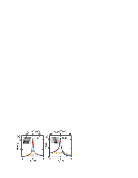
Figure 1 (a)-(b) shows dc two-point resistance data, , versus gate voltage, , which controls the charge density, (upper axis) for Samples A and B respectively. From the width of the maximum at low , we extract a half-width-half-maximum, HWHM, of 0.45 and 0.95 V for Samples A and B. These HWHMs correspond to an impurity induced charge density of 1.5 and 2.1 cm-2. For clarity, the data in Fig. 1 is slightly shifted along the axis so that all the maxima (Dirac points) line up at 0, the shifts in panel (a) range from -0.3 to -0.45 V at various , and in panel (b) from 0 to 0.2 V. The insets in Fig. 1 show scanning electron microscope (SEM) tilted images of Sample A and a sample identical to Sample B.
We confirmed, using optical contrast and Raman spectroscopy, that both samples are single-layer graphene. Sample A is 650 nm long, 675 nm wide, and suspended 140 10 nm above the substrate (AFM measurement) which consists of 100 2 nm of SiO2 (ellipsometry measurement) on degenerately-doped Si which is used as a back-gate electrode. Sample B is 400 nm long, 0.97 m wide, and suspended 227 10 nm above a 74 2 nm SiO2 film on Si. To prepare the samples, we used exfoliated graphene, and standard e-beam lithography to define Ti(5nm)/Au(80nm) contacts. The samples were suspended with a wet BOE etch such that their only thermal connection was to the gold contacts. We annealed the devices using Joule heating in situ by flowing a large current in the devicesBolotin et al. (2008); Yigen et al. (2013) (see Supplemental Information (SI) section 1). Annealing and all subsequent measurements were done under high vacuum, Torr.
To minimize contact resistance, , the devices were fabricated with large contact areas between the gold electrodes and graphene crystals, ranging from 1.1 to 3 per contact. An upper bound for series resistance, , which includes both the contact resistance, , and the resistance from neutral scatterers, can be extracted from the two-point curvesDean et al. (2010) in Fig. 1 (see SI section 2). The extracted series resistances for Sample A are 477 53 and 944 80 for hole and electron doping, respectively. The difference between and is understood as an additional barrier for the electron due to doping from the gold electrodes Castro et al. (2010). For Sample B, we find 1563 and 812 . We note that series resistance is smallest for hole doping in Sample A and for electron doping in Sample B. In annealed samples, oxygen desorbs from the gold contacts and changes the work function of the electrodes. This means that graphene under the gold electrodes can be either electron doped or hole doped depending on the thoroughness of the contact annealingCastro et al. (2010); Heinze et al. (2002); Giovannetti et al. (2008). To minimize the effect of on our data, we study the lowest resistance side of the Dirac point for each Sample. This allows us to study hole transport in Sample A and electron transport in Sample B. Since includes both and the resistance due to neutral scatterers in the channel, we conservatively set = with an uncertainty ranging up to , and down to lowest reported resistance for Au/grapheneIfuku et al. (2013) with similar , which is 100 m2. Thus, in the following data analysis we use for Samples A and B, 239 and 406 . We extract a conservative estimate of the charge carrier mobility in our devices, over the and range studied, as 3.5 10 4 cm2/V.s, where is the total carrier density including the gate, impurity and thermal doping Dorgan, Bae, and Pop (2010); Yigen et al. (2013) (SI section 3). Based on the reported thermal conductance of Au/Ti/Graphene and Graphene/SiO2 interfacesKoh et al. (2010), the thermal resistance of the contacts can safely be neglectedDorgan et al. (2013) compared to our data presented below.
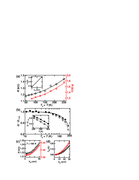
Figure 2 summarizes our approach to extract in suspended high-mobility graphene, whose details we previously discussed Yigen et al. (2013). We repeat some of the discussion of our methods because the charge densities studied here are much higher than in Ref. 6, which leads to several important changes. Figure 2(a)-(b) presents how we monitor the charged quasiparticle temperature in our devices by monitoring , and Fig. 2(c)-(d) shows how we can controllably heat-up these quasiparticles at a temperature slightly above the contacts’ temperature via Joule heating. By combining these two capabilities and using the heat equation, we will later extract vs and .
Figure 2(a) shows the two-point dc vs cryostat temperature, , calibration curves for Sample A (circles, left axis), and Sample B (squares, right axis) which are respectively hole-doped with a gate-induced density of -1.8 cm-2 and electron-doped with 1.1 cm-2. is extracted from the slope of the dataRno as shown in the inset of Fig. 2(a). Note that for 1 mV bias no Joule heating effect is present and . The dependence of the data shows a metallic behavior with increasing with . The interpolated lines in Fig. 2(a), and similar curves, will be used as secondary thermometry curves to monitor in the devices.
Figure 2(b) shows the relative conductance for Sample A extracted from Fig. 2(a) and similar data. The solid circles show the raw two-point data, and the open circles the data after subtracting . The dependence of in graphene, at modest charge density, is strongly dependent on the type of charge transport. We fit the data in Fig. 2(b) with a function , and extract = 2.1 0.2 for both curves. This -dependence strongly supports diffusive charge transport dominated by long-range charge impurities, as reported in previous experiments on high-mobility devices Bolotin et al. (2008); Du et al. (2008); Das Sarma et al. (2011) and expected theoretically Das Sarma and Hwang (2013). The inset of Fig. 2(b) shows that of Sample A decreases linearly for 200 K, which suggests a relatively strong acoustic phonon scattering above this temperature, as expected theoretically Das Sarma and Hwang (2013). Sample B shows a qualitatively identical behavior of its vs in Fig. 2(a), but the absence of low temperature data proscribes an accurate fit of its dependence. We will focus our measurements on the 200 K range, where both samples are in the diffusive regime (SI section 3) with scattering predominantly due to charged impurities. This scattering is elastic, and its dependence (used for thermometry) comes mostly from the temperature dependence of its screening Das Sarma et al. (2011).
Electron-electron scattering between charge carriers is inelastic. By applying a one can inject high-energy carriers in the suspended device which then thermalize with the carriers in the sample and raise in the suspended graphene relative to the temperature in the gold contacts. Note that when writing , we always refer to the average temperature of charged quasiparticles in our devices. We demonstrate controlled Joule self-heating of the electrons to apply a thermal bias between the suspended graphene and the electrodes (cryostat temperature). Figure 2(c) shows vs for Sample A at 100 K and -1.8 1011 (circles, left axis) and -0.8 cm-2 (squares, right axis). Sample B data is shown in SI sec. 4. increases monotonically with increasing , at all . We restrict our measurements to meV. We have previously arguedYigen et al. (2013) that in our high-mobility devices, under such low and in the range we study, the change in is caused by Joule heating of the charge carriersViljas et al. (2011); Yigen et al. (2013). Using the curves, vs and vs , we extract vs as shown for Sample A in Fig. 2(d). We fit a power law (dashed lines) , and find 1.93 0.04 for both data sets, as expected for Joule heating where . Figures 3(d) and S3(b) show that the accuracy with which can be extracted is much better than 1 K. The smooth dependence of on at all is consistent with electrons having a well defined temperature as predicted by calculations of the collision lengthLi and Das Sarma (2013) (see SI of Ref. 6), and confirmed by the data shown below.
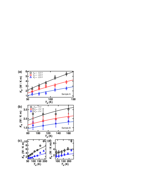
We use a 1-d heat equationYigen et al. (2013) to extract in our devices, and find , where , is the Joule heating power per unit volume, the width, the length, = 0.335 nm the thickness, and is the electronic temperature averaged over . In Fig. 3(a)-(b) we plot vs for Samples A and B for = 10 K, where the circle, square and triangle data show at -1.8, -1.1, -0.8 cm-2 for Sample A, and 1.1, 0.7, 0.5 cm-2 for Sample B. The quantity refers to the total charge density induced by and charged impurities (SI section 3). We clearly observe that increases with both and in both samples. For instance, ranges from roughly 1 W/K.m at 60 K and -8 1010cm-2 to 5 W/K.m at 135 K and -1.8 1011cm-2 for Sample A. Error bars representing the uncertainty on the extracted are shown in Fig. 3 (SI section 5). We confirmed that the needed to create did not dope significantly the samples or affect the measured VBn . The thermoelectric voltages in our devices are negligible compared to Zuev, Chang, and Kim (2009); Hwang, Rossi, and Das Sarma (2009).
We test the WF law in our samples, which have a mobility of 3.5 10 4 cm2/V.s, as a function of and . While the Lorenz number in most metals is close to 2.44 10-8 , it is well known that its value can be reduced in semiconductors at low charge density Bian et al. (2007); Minnich et al. (2009). The solid lines in Fig. 3 show given by the WF law using the measured and extracted (Fig. 2), with used as the single fitting parameter. The WF relation holds for both Samples at all between 50 K and 160 K, and densities -1.8 to -0.8 cm-2 and 0.5 to 1.1 cm-2. For Sample A, 0.45, 0.53 and 0.55 , and for Sample B 0.66, 0.68, 0.7 (triangle, square, and circle data, respectively). The main uncertainty on comes from the uncertainty on , and corresponds to for Sample A, and 0.4 for Sample B. We note that the qualitative temperature and density dependence of the data in Fig. 3, and the agreement with the WF law, is preserved even if we use either the maximum or minimum 120 (SI section 6). The increase in as increases is consistent with previous studies in semiconductors where the value of tends toward at higher carrier density Minnich et al. (2009).
Electron to acoustic phonon coupling is very weak in clean graphene at moderate doping and temperature ( 200 - 300 K) Gabor et al. (2011); Song et al. (2011); Viljas et al. (2011); Yigen et al. (2013); Das Sarma and Hwang (2013), but increases at higher and . In the context of our experiment, if the thermal energy conductance between electrons and phonons is non-negligeable compared to the electronic thermal conductance , the heat conductivity we extract is a mixture of and in parallel. As can be seen in Fig. 3(c)-(d), above 160 K the extracted no longer agrees with the WF prediction (solid line), indicating that we cannot isolate for . Previously we found that we could extract up to 300 K in samples whose was very close to the CNP Yigen et al. (2013), suggesting that coupling is weaker at lower as expected theoreticallyDas Sarma and Hwang (2013). In Fig. 3(c)-(d), the departure between the data and WF prediction starts around 150 K for Samples A and 200 K for Sample B. The different ranges over which dominates in the two devices comes from the ratio which is 60 larger for Sample B than Sample A.
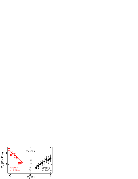
Figure 4 shows the extracted vs at K for Sample A (B) as solid red squares (black circles). For reference only, we also show two data points (open grey symbols) close to 0 which are taken from Ref. 6 for the same Samples. We cannot extract at intermediate , i.e. when 0.3 V 1.5 V. This is because while smoothly increases with in the metal-like regime (Fig. 2(a)), 1.5 V, and smoothly decrease in the insulator-like regimeYigen et al. (2013), 0.3 V, the vs behavior does not act as a good thermometer at intermediate densities. We also note that the WF relation we discuss in this work, , only applies in the degenerately doped regime where the Fermi energy , and we focus our discussion on this regime. The solid symbol data in Fig. 4 show that is tuned by the charge carrier density in the samples. The solid lines are the WF values calculated using the measured , 110 K, and setting = 0.53 and 0.67 for Samples A and B. The agreement between the WF law and data in the doped regime is excellent. Even using a modest range, could be tuned by a factor of 2 in Fig. 4. This is a very strong thermal-transistor effect (with the caveat that Balandin (2011); Pop, Varshney, and Roy (2012)). This could have applications in optoelectronics. A larger means that when a charge carrier is excited by a photon, it can travel a larger distance and excite additional carriers before it thermalizes with the lattice. Thus, more of the photon energy is harvested as electrical current Tielrooij et al. (2013). Additionally, a tunable implies a tunable which could be used to optimize bolometric applications of graphene Fong and Schwab (2012); Fong et al. (2013).
In summary, we fabricated high quality suspended graphene devices. We used a self-thermometry and self-heating method Yigen et al. (2013) to extract the electronic thermal conductivity in doped graphene. We report for the first time in suspended graphene over a broad range of and . The data presented clearly demonstrates that , which confirms that the Wiedemann-Franz law holds in high-mobility ( 3.5 10 4 cm2/V.s) suspended graphene over our accessible temperature range, 50 K - 160 K. This temperature range is limited at high-temperature by a turning on of the electron-phonon coupling, which prevents us from isolating at higher . The clear onsets of the electron-phonon coupling (Fig. 2(b), and 3(c)-(d)) between 150 K- 200K is consistent with theoretical calculations Das Sarma and Hwang (2013). We studied charge densities of holes and electrons ranging up to 1.8 1011 cm-2 and found Lorenz numbers 0.5 - 0.7 , where is the standard Lorenz number for metals. The quality of the agreement between the data and the WF relation in Figs. 3 and 4 is not affected by the uncertainty on the extracted Lorenz numbers (SI section 6). Finally, we demonstrated a strong thermal-transistor effect where we could tune by more than a factor of 2 by applying only a few volts to a gate electrode.
In the future, these measurements could be extended to even cleaner devices at lower densities to study possible corrections to the generalized WF relation due to strong electron-electron interactionsMuller, Fritz, and Sachdev (2008); Foster and Aleiner (2009). The demonstrated density control of could be useful to make energy harvesting optoelectronic devices Song et al. (2011); Gabor et al. (2011); Tielrooij et al. (2013) and sensitive bolometersFong and Schwab (2012); Fong et al. (2013). We thank Vahid Tayari, James Porter and Andrew McRae for technical help and discussions. This work was supported by NSERC, CFI, FQRNT, and Concordia University. We made use of the QNI cleanrooms.
References
- Gabor et al. (2011) N. M. Gabor, J. C. W. Song, Q. Ma, N. L. Nair, T. Taychatanapat, K. Watanabe, T. Taniguchi, L. S. Levitov, and P. Jarillo-Herrero, Science 334, 648 (2011).
- Song et al. (2011) J. C. W. Song, M. S. Rudner, C. M. Marcus, and L. S. Levitov, Nano Lett. 11, 4688 (2011).
- Viljas et al. (2011) J. K. Viljas, A. Fay, M. Wiesner, and P. J. Hakonen, Phys. Rev. B 83, 205421 (2011).
- Fong and Schwab (2012) K. C. Fong and K. C. Schwab, Phys. Rev. X 2, 031006 (2012).
- Das Sarma and Hwang (2013) S. Das Sarma and E. H. Hwang, Phys. Rev. B 87, 035415 (2013).
- Yigen et al. (2013) S. Yigen, V. Tayari, J. O. Island, J. M. Porter, and A. R. Champagne, Phys. Rev. B 87, 241411 (2013).
- Tielrooij et al. (2013) K. J. Tielrooij, J. C. W. Song, S. A. Jensen, A. Centeno, A. Pesquera, A. Z. Elorza, M. Bonn, L. S. Levitov, and F. H. L. Koppens, Nature Physics 9, 248–252 (2013).
- Fong et al. (2013) K. C. Fong, E. Wollman, R. Ravi, W. Chen, A. A. Clerk, M. D. Shaw, H. G. Leduc, and K. C. Schwab, arXiv: 1308.2265 (2013).
- Saito, Nakamura, and Natori (2007) K. Saito, J. Nakamura, and A. Natori, Phys. Rev. B 76, 115409 (2007).
- Muller, Fritz, and Sachdev (2008) M. Muller, L. Fritz, and S. Sachdev, Phys. Rev. B 78, 115406 (2008).
- Foster and Aleiner (2009) M. S. Foster and I. L. Aleiner, Phys. Rev. B 79, 085415 (2009).
- Bolotin et al. (2008) K. I. Bolotin, K. J. Sikes, Z. Jiang, M. Klima, G. Fudenberg, J. Hone, P. Kim, and H. L. Stormer, Solid State Comm. 146, 351 (2008).
- Dean et al. (2010) C. R. Dean, A. F. Young, I. Meric, C. Lee, L. Wang, S. Sorgenfrei, K. Watanabe, T. Taniguchi, P. Kim, K. L. Shepard, and J. Hone, Nature Nanotechnol. 5, 722 (2010).
- Castro et al. (2010) E. V. Castro, H. Ochoa, M. I. Katsnelson, R. V. Gorbachev, D. C. Elias, K. S. Novoselov, A. K. Geim, and F. Guinea, Phys. Rev. Lett. 105, 266601 (2010).
- Heinze et al. (2002) S. Heinze, J. Tersoff, R. Martel, V. Derycke, J. Appenzeller, and P. Avouris, Phys. Rev. Lett. 89, 106801 (2002).
- Giovannetti et al. (2008) G. Giovannetti, P. A. Khomyakov, G. Brocks, V. M. Karpan, J. van den Brink, and P. J. Kelly, Phys. Rev. Lett. 101, 026803 (2008).
- Ifuku et al. (2013) R. Ifuku, K. Nagashio, T. Nishimura, and A. Toriumi, arXiv: 1307.0690 (2013).
- Dorgan, Bae, and Pop (2010) V. E. Dorgan, M. H. Bae, and E. Pop, Appl. Phys. Lett. 97, 082112 (2010).
- Koh et al. (2010) Y. K. Koh, M. H. Bae, D. G. Cahill, and E. Pop, Nano Lett. 10, 4363 (2010).
- Dorgan et al. (2013) V. E. Dorgan, A. Behnam, H. J. Conley, K. I. Bolotin, and E. Pop, Nano Lett. 13, 4581 (2013).
- (21) As showed in Fig. 2(a)-inset, the characteristics at very low are precisely linear (no Joule heating). In which case , and we use the slope to extract to avoid an error due to a very small (experimental) offset in (few 10s of micro-Volt). At higher bias, this small offset is negligible and we can safely use . In Figure 2(c), is not constant versus due to Joule heating, thus also contains information about how quickly the temperature is changing with , rather than only the temperature at one specific value. Since () is small, we find no significant quantitative difference in our results using either or to extract , but the correct quantity which represents is . .
- Du et al. (2008) X. Du, I. Skachko, A. Barker, and E. Y. Andrei, Nature Nanotech. 3, 491–495 (2008).
- Das Sarma et al. (2011) S. Das Sarma, S. Adam, E. H. Hwang, and E. Rossi, Rev. Mod. Phys. 83, 407 (2011).
- Li and Das Sarma (2013) Q. Li and S. Das Sarma, Phys. Rev. B 87, 085406 (2013).
- (25) Using (SM section 3)Dorgan, Bae, and Pop (2010); Yigen et al. (2013), we define an effective chemical potential . For instance, for Sample A at -5.3 V and = 100 K, 49 meV. The various necessary to achieve 10 K in Fig. 3 are always significantly smaller than and never larger than 27 mV. We only observe a change in the extracted values (in the doped-regime) when exceeds 20 K, and . .
- Zuev, Chang, and Kim (2009) Y. M. Zuev, W. Chang, and P. Kim, Phys. Rev. Lett. 102, 096807 (2009).
- Hwang, Rossi, and Das Sarma (2009) E. H. Hwang, E. Rossi, and S. Das Sarma, Phys. Rev. B 80 (2009).
- Bian et al. (2007) Z. Bian, M. Zebarjadi, R. Singh, Y. Ezzahri, A. Shakouri, G. Zeng, J. H. Bahk, J. E. Bowers, J. M. O. Zide, and A. C. Gossard, Phys. Rev. B 76, 205311 (2007).
- Minnich et al. (2009) A. J. Minnich, M. S. Dresselhaus, Z. F. Ren, and G. Chen, Energy and Environmental Science 2, 466 (2009).
- Balandin (2011) A. A. Balandin, Nature Mater. 10, 569 (2011).
- Pop, Varshney, and Roy (2012) E. Pop, V. Varshney, and A. K. Roy, MRS Bulletin 37, 1273 (2012).