Metal oxide resistive switching: evolution of the density of states across the metal-insulator transition
Abstract
We report the study of metal-STO-metal memristors where the doping concentration in STO can be fine-tuned through electric field migration of oxygen vacancies. In this tunnel junction device, the evolution of the Density Of States (DoS) can be followed continuously across the Metal-Insulator Transition (MIT). At very low dopant concentration, the junction displays characteristic signatures of discrete dopants levels. As the dopant concentration increases, the semiconductor band gap fills in but a soft Coulomb gap remains. At even higher doping, a transition to a metallic state occurs where the DoS at the Fermi level becomes finite and Altshuler-Aronov corrections to the DoS are observed. At the critical point of the MIT, the DoS scales linearly with energy , the possible signature of multifractality.
pacs:
73.20.At,71.23.Cq,73.20.FzMemristive devices have attracted considerable attention since the recognition that two-terminals resistive switching devices Strukov et al. (2008) represent an example of a memristive element, whose existence was hypothesized by L. Chua in 1971. Numerous works on binary metal oxides MOx and STO, see Refs. Dearnaley et al. (1970); Yang et al. (2013); Waser and Aono (2007) for review, have demonstrated that resistance switching is due to the electric-field induced migration of positively charged oxygen vacancies. This anion migration leads to a change in the metal cation valence and therefore to a change in the band occupation Yang et al. (2008). In titanium based oxide materials, the oxidation number of the titanium cation changes from +IV to +III which corresponds to n-type doping. Doping dependency studies of semiconductors have been essential for the understanding of the Anderson localisation and the interplay between Coulomb interactions and disorder in the vicinity of MITs Belitz and Kirkpatrick (1994); Lee (1985). While past works usually relied on the study of samples with fixed doping levels Lee (2004); Bielejec et al. (2001); Lee et al. (1999); Massey and Lee (1996); McMillan and Mochel (1981), we found that electric field induced migration of oxygen vacancies at very low temperature allows fine tuning of the dopants concentration from the insulating to the metallic regime. This makes resistive switching devices a remarkable tool for the study of MITs.
We present a study of MIT in STO through electric field induced migration of oxygen vacancies at very low temperature (). STO is a material with good oxygen mobility whose resistive switching properties have been much studied Yang et al. (2008); Andreasson et al. (2009); Waser et al. (2009); Andreasson et al. (2007); Janousch et al. (2007); Szot et al. (2006); Meijer et al. (2005) where it has been demonstrated that nano-sized conducting filaments down to a single dislocation could be obtained Szot et al. (2006). On a (110) oriented STO substrate, two electrodes of width separated by a distance of are deposited, Fig. 1a. A conducting filament is formed at room temperature, as illustrated Fig. 1a, by ramping up the voltage until a resistance switching is observed, Fig. 1c. This is the so-called forming step where oxygen vacancies accumulate along some percolating path between the two electrodes. This leads to a junction of resistance of only a few hundred Ohms, which is nearly temperature independent down to low temperature where it starts to decrease below , Fig. 1d, indicating the apparition of superconductivity. Indeed, doped STO is known to become superconducting in this temperature rangeKoonce and Cohen (1967), with for a carrier concentration of the order of , Ref. Ueno et al. (2011).
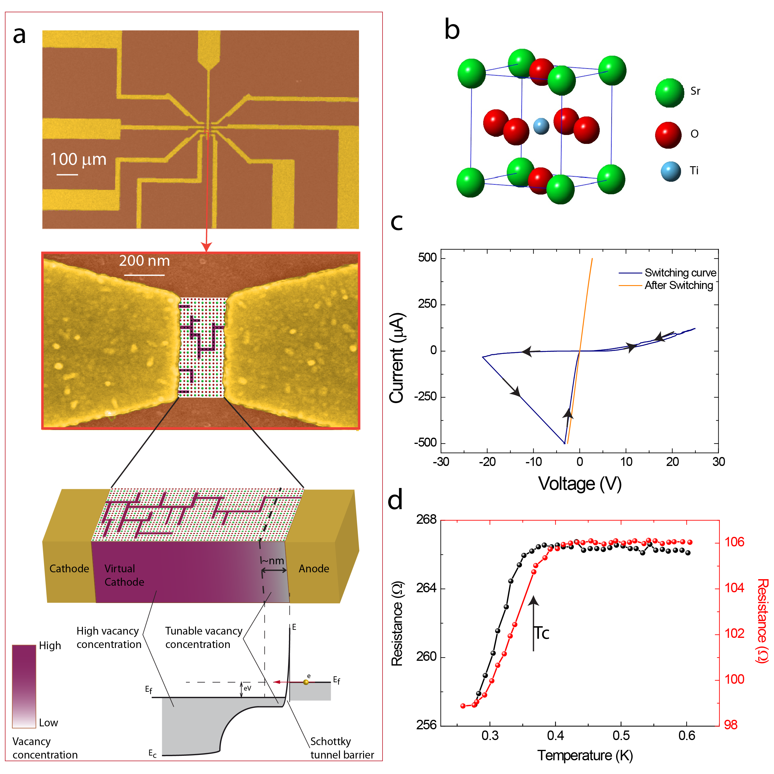
At low temperature (), the conductance of this junction decreases by 5 orders of magnitude upon applying a single positive voltage pulse, of magnitude 5 V and duration 1 ms, Fig. 2a. In figure 2, each differential conductance shown is measured at small voltage bias just after a voltage pulse has been applied. Up to 1600 pulses followed by measurements of the differential conductance have been realized for this junction.
As the junction is now insulating, applying negative voltage pulses moves the vacancies in the opposite direction and leads now to an increase of the conductance, up to 5 orders of magnitude, Fig. 2. Upon reaching a high differential conductance, , a single positive voltage pulse () is applied again, which switches the junction insulating once more. This protocol can be executed many times – up to 10 times for this junction. For each run, the junction is tuned from insulating to the conducting state by applying negative voltage pulses of small magnitude. Between each run, a positive pulse is applied to turn the junction insulating.

We argue now that the effect of the voltage pulses is to migrate the oxygen vacancies only in a narrow region in close proximity to the electrode. First, this experiment is performed at low temperature where thermal activated migration of ions is completely inhibited and vacancy motion is due to electric-field activated migration of ions. As electric-field induced migration of ions can only occur on a length of the order of the Debye screening length, and because the screening length is short in conducting filaments, ions migration only occurs on a short length scale. This leads to a device with characteristics depicted Fig. 1a, where a nanosized region of weakly doped STO is located between two conducting electrodes. This picture is consistent with previous explanations of memristive behaviors in titanium oxide based devices where the resistance switching is believed to occur in the immediate vicinity of the electrodes. The weakly doped STO nanosized region is connected on one side by an ohmic contact to a highly doped-STO electrode, and, on the other side, is connected by a Schottky barrier to the gold electrode, where the Schottky barrier makes a tunnel barrier for electrons Wolf (2011). At low doping, the barrier height is given by the energy difference between the works functions of STO , ref. Zagonel et al. (2009) and gold , ref. Huber (1966), which gives . As we will see below, features of interest in the DoS are located at low energy, , implying that the IV curves can be interpreted as DoS curves. As the doping concentration increases in this n-doped semiconductor, the barrier height increases, while its width decrease Sze and Ng (2007), and so the junction remains in the tunneling regime. In this geometry, the differential conductance curves shown Fig. 2 represent, at low voltage, , the DoS of the weakly doped region:
| (1) |
When a voltage of positive polarity is applied, oxygen vacancies are repelled at the junction and the DoS decreases, for a voltage pulse of negative polarity, oxygen vacancies accumulate at the junction and the DoS increases. Within a single run, sudden jumps of conductance are occasionally observed, as observed Fig. 2f. They correspond to resistance switching usually observed in memristive devices. These jumps do not appear to be correlated with any specific values of the conductance. As the 6 different runs shown in Fig. 2 are plotted together, Fig. 2g, we can see, first: that similar conductance curves can be reproduced even after a full cycle from insulating to conducting, which indicates that doping can be tuned reversibly in those junctions; second, that the junction conductance can be tuned continuously to any value as shown by the plot of conductance at zero bias for all measured conductance curves, Fig. 2h. A detailed look at the differential conductance curves taken at different conductance values allows to clearly characterize the evolution of the DoS in STO as a function of doping, Fig. 3.
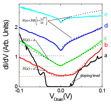
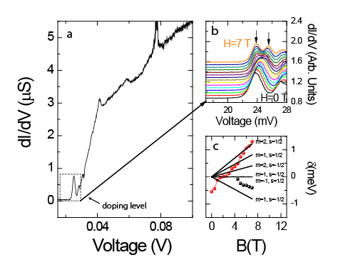
At the lowest doping, shows a sharp gap and well resolved peaks at voltage values (, , ). These peaks, which have been observed in a second sample (Fig. S1), correspond to discrete doping levels. Applying a magnetic field leads to a Zeeman splitting of the peaks, Fig. 4, which can be fitted approximately by the relation , using for the orbital quantum numbers and for the spin quantum numbers . As the orbital number has to be included to fit the Zeeman splitting, this indicates that this discrete doping level arises from doped electronic states into the conduction band composed of the , and titanium orbitals Mattheiss (1972). This is further confirmed by the observation that this state is located just below the gap edge as expected for n-type dopants. Only samples annealed at high temperatureLee et al. (1975); Spinelli et al. (2010) have hydrogenic donor levels located very close to the conduction band. In non-annealed samples, as in our case, from an analysis of the temperature dependence of the Hall coefficientTufte and Chapman (1967); Lee et al. (1975) and the observation of sharp peaks in optical absorption spectrumLee et al. (1975), it has been concluded that the oxygen vacancies levels may be located almost anywhere from nearly zero to about below the conduction band, as observed in our tunneling spectrum.
While the observation of individual dopant states was attempted through the formation of nano-sized Schottky diodes Smit et al. (2004); Calvet et al. (2002) and nanosized field effect transistors Calvet et al. (2011, 2007), we find that the use of oxide semiconductors, with its possibility of fine-tuning the dopant concentration in-situ at low temperature, offers a remarkable tool for the study of individual dopant states. We show now this method allows studying the MIT as a function of doping with unprecedented resolution. As the doping concentration increases, the gap fills in and sharp features disappear, however, a soft gap remains where the DoS vanishes at the Fermi level with the quadratic form in 3D, due to Coulomb interactions as shown by Efros and Shklovskii Efros and Shklovskii (1975). Such a soft gap was observed previously in doped semiconductors through tunneling spectroscopy Lee (2004); Bielejec et al. (2001); Lee et al. (1999); Massey and Lee (1996); McMillan and Mochel (1981). As the dopant concentration increases, the soft gap closes and a transition to a metallic regime occurs. In the metallic regime, the DoS is finite at the Fermi level and a cusp, in 3D, is observed, where the correlation energy parameter , i.e. the Thouless energy, depends on the diffusion constant and the electron mean free path . This cusp is due to the exchange part of the Coulomb interactions as shown by McMillan McMillan (1981), Altshuler and Aronov Altshuler and Aronov (1979). Fitting the data shows that decreases at the approach of the transition, as expected when the electronic states at the Fermi level gets more and more localized. The maximum value found for can be explained assuming the reasonable values for and . Finally, just at the transition, the critical DoS follows a linear behaviour, . The question of the energy dependence of the critical DoS remains one of the major theoretical question of the Mott-Anderson MIT Belitz and Kirkpatrick (1994). A theoretical prediction suggests Lee et al. (1999) that the DoS should follow ; this implies that , which is within the bounds 13 , as theoretically expected McMillan and Mochel (1981). This power law suppression of the DoS at criticality is a signature of multifractality, a remarkable property of electronic wavefunctions near the MITEvers and Mirlin (2008). Recent theoretical works have found that multifractality persists even in presence of Coulomb interactionsBurmistrov et al. (2013); Amini and Kravtsov and multi-fractal characteristics have been found in STM spectroscopy measurements of Ga1-xMnxAsRichardella et al. (2010).
Note that the DoS curves were compared with theoretical predictions assuming tri-dimensionality. Indeed, while previous worksWaser and Aono (2007); Yang et al. (2013) have shown that the vacancies are distributed along filamentary paths, we don’t expect that quantum confinement effects would alter the 3D band structure of STO along the filament. For this reason, we can assume that the effect of doping is to inject carriers into the 3D band structure of STO.
While we don’t have a direct measure of the oxygen vacancy concentration, we can estimate that this concentration changes from nearly zero, where single impurity levels are observed, to , where the superconducting transition temperature is maximumUeno et al. (2011). The MIT should be at concentrations below according to results from Spinelli et al. Spinelli et al. (2010).
We thank M. Rosticher and J. Palomo for their help with clean room works. We acknowledge support from ANR grant ”QUANTICON” 10-0409-01 and ANR Grant ”CAMELEON” 09-BLAN-0388-01.
References
- Strukov et al. (2008) D. B. Strukov, G. S. Snider, D. R. Stewart, and R. S. Williams, Nature 453, 80 (2008).
- Dearnaley et al. (1970) G. Dearnaley, a. M. Stoneham, and D. V. Morgan, Reports on Progress in Physics 33, 1129 (1970).
- Yang et al. (2013) J. J. Yang, D. B. Strukov, and D. R. Stewart, Nature nanotechnology 8, 13 (2013).
- Waser and Aono (2007) R. Waser and M. Aono, Nature materials 6, 833 (2007).
- Yang et al. (2008) J. J. Yang, M. D. Pickett, X. Li, D. a. a. Ohlberg, D. R. Stewart, and R. S. Williams, Nature nanotechnology 3, 429 (2008).
- Belitz and Kirkpatrick (1994) D. Belitz and T. Kirkpatrick, Reviews of Modern Physics 66, 261 (1994).
- Lee (1985) P. A. Lee, Reviews of Modern Physics 57, 287 (1985).
- Lee (2004) M. Lee, Physical Review Letters 93, 1 (2004).
- Bielejec et al. (2001) E. Bielejec, J. Ruan, and W. Wu, Physical Review Letters 87, 036801 (2001).
- Lee et al. (1999) M. Lee, J. Massey, V. Nguyen, and B. Shklovskii, Physical Review B 60, 1582 (1999).
- Massey and Lee (1996) J. Massey and M. Lee, Physical Review Letters 77, 3399 (1996).
- McMillan and Mochel (1981) W. McMillan and J. Mochel, Physical Review Letters 46, 556 (1981).
- Andreasson et al. (2009) B. P. Andreasson, M. Janousch, U. Staub, and G. I. Meijer, Applied Physics Letters 94, 013513 (2009).
- Waser et al. (2009) R. Waser, R. Dittmann, G. Staikov, and K. Szot, Advanced Materials 21, 2632 (2009).
- Andreasson et al. (2007) B. Andreasson, M. Janousch, U. Staub, G. Meijer, and B. Delley, Materials Science and Engineering: B 144, 60 (2007).
- Janousch et al. (2007) M. Janousch, G. I. Meijer, U. Staub, B. Delley, S. F. Karg, and B. P. Andreasson, Advanced Materials 19, 2232 (2007).
- Szot et al. (2006) K. Szot, W. Speier, G. Bihlmayer, and R. Waser, Nature materials 5, 312 (2006).
- Meijer et al. (2005) G. Meijer, U. Staub, M. Janousch, S. Johnson, B. Delley, and T. Neisius, Physical Review B 72, 155102 (2005).
- Koonce and Cohen (1967) C. S. Koonce and M. L. Cohen, Physical Review 163, 380 (1967).
- Ueno et al. (2011) K. Ueno, S. Nakamura, H. Shimotani, H. T. Yuan, N. Kimura, T. Nojima, H. Aoki, Y. Iwasa, and M. Kawasaki, Nature nanotechnology 6, 408 (2011).
- Wolf (2011) E. L. Wolf, Principles of Electron Tunneling Spectroscopy:Second Edition, Vol. 2011 (Oxford University Press, 2011) p. 616.
- Zagonel et al. (2009) L. F. Zagonel, M. Bäurer, a. Bailly, O. Renault, M. Hoffmann, S.-J. Shih, D. Cockayne, and N. Barrett, Journal of physics. Condensed matter : an Institute of Physics journal 21, 314013 (2009).
- Huber (1966) E. E. Huber, Applied Physics Letters 8, 169 (1966).
- Sze and Ng (2007) S. M. Sze and K. K. Ng, Physics of semiconductor devices, Wiley-Interscience publication (Wiley-Interscience, 2007).
- Mattheiss (1972) L. Mattheiss, Physical Review B 6, 4718 (1972).
- Lee et al. (1975) C. Lee, J. Destry, and J. Brebner, Physical Review B 11, 2299 (1975).
- Spinelli et al. (2010) a. Spinelli, M. a. Torija, C. Liu, C. Jan, and C. Leighton, Physical Review B 81, 1 (2010).
- Tufte and Chapman (1967) O. Tufte and P. Chapman, Physical Review 155, 796 (1967).
- Smit et al. (2004) G. Smit, S. Rogge, J. Caro, and T. Klapwijk, Physical Review B 69, 035338 (2004).
- Calvet et al. (2002) L. E. Calvet, R. G. Wheeler, and M. a. Reed, Applied Physics Letters 80, 1761 (2002).
- Calvet et al. (2011) L. E. Calvet, J. P. Snyder, and W. Wernsdorfer, Physical Review B 83, 205415 (2011).
- Calvet et al. (2007) L. Calvet, R. Wheeler, and M. Reed, Physical Review Letters 98, 096805 (2007).
- Efros and Shklovskii (1975) A. L. Efros and B. I. Shklovskii, Journal of Physics C: Solid State Physics 8, L49 (1975).
- McMillan (1981) W. McMillan, Physical Review B 24, 2739 (1981).
- Altshuler and Aronov (1979) B. Altshuler and A. Aronov, Solid State Communications 30, 115 (1979).
- Evers and Mirlin (2008) F. Evers and A. Mirlin, Reviews of Modern Physics 80, 1355 (2008).
- Burmistrov et al. (2013) I. S. Burmistrov, I. V. Gornyi, and a. D. Mirlin, Physical Review Letters 111, 066601 (2013).
- (38) M. Amini and V. E. Kravtsov, cond-mat/ , 1arXiv:1305.0242v2 .
- Richardella et al. (2010) A. Richardella, P. Roushan, S. Mack, B. Zhou, D. a. Huse, D. D. Awschalom, and A. Yazdani, Science (New York, N.Y.) 327, 665 (2010).