Silicane and germanane: tight-binding and first-principles studies
Abstract
We present a first-principles and tight-binding model study of silicane and germanane, the hydrogenated derivatives of two-dimensional silicene and germanene. We find that the materials are stable in freestanding form, analyse the orbital composition, and derive a tight-binding model using first-principles calculations to fit the parameters.
pacs:
73.20.-r, 71.15.MbRecent years have seen a rapid rise in research interest towards atomically thin two-dimensional (2D) materials. Graphene has been in the focus of intensive research since its discovery [1, 2], followed by silicene, Si2 [3, 4, 5, 6]. Practical application of graphene in nanoelectronics is somewhat limited by the lack of a band gap, and while alternatives such as hexagonal boron nitride [7, 8] and transition metal dichalcogenides [9, 10, 11, 12, 13, 15, 14] exist and others have been predicted theoretically such as gallium chalcogenides [16], significant research effort has been put into engineering a band gap in graphene. Complete hydrogenation was shown to be another way to engineer a band gap in graphene. The resulting material, graphane [17] (C2H2) has a buckled honeycomb structure with a single hydrogen atom attached to each carbon site on alternating sides of the sheet. A recent experiment [18] has shown that few-layer germanane (Ge2H2), the hydrogenated germanene, can be synthesised, expanding the family of atomic 2D materials.
In this work we provide a first-principles study of silicane and germanane. We present the phonon dispersions to illustrate that these materials are dynamically stable. The band structures, effective masses, charge carriers, and an orbital decomposition of the valence and conduction bands at high symmetry points in the Brillouin zone are presented. The latter information is utilised for building a tight-binding model for the description of the valence and conduction bands of silicane and germanane.
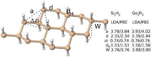
(I) Silicane and germanane have a honeycomb lattice as depicted in Fig. 1. The unit cell comprises two Si/Ge atoms and two H atoms, and the A and B sublattices of Si/Ge atoms exhibit a buckling. The tight-binding model we employ is an all-valence second-nearest neighbour model that takes into account four (one and three ) electrons per Si/Ge atom and the single electron of hydrogen. The tight-binding Hamiltonian is
Here, and are the creation and annihilation operators of the electrons of Si/Ge, and are the same for the electrons of Si/Ge, while and are the same for the electrons of the H atoms. In , parameters and are the on-site energies of the and orbitals of Si/Ge, is the on-site energy of the electron of the hydrogen atom. In , parameterises the nearest neighbour hopping between orbitals of Si/Ge and hydrogen, while , , , and are the nearest neighbour hoppings between Si/Ge electrons on sublattice A and sublattice B. In , parameters , , , and are the second-nearest neighbour hoppings between the Si/Ge electrons on the same sublattice, while and are the second-nearest neighbour hoppings between the orbitals of Si/Ge and hydrogen on different sublattices. Summations in go over the A and B sublattices while summations in and go over ; ,, and take into account the orientation of the orbitals, where denotes the coordinates of the atoms. The Hamiltonian in the Slater–Koster approach [19], shown with solid lines separating A and B sublattice contributions as well as hydrogen contributions has the form of a matrix:
The total number of parameters in this model is sixteen, but one can choose one of the on-site energies to be zero to set the Fermi level leaving fifteen parameters to fit. The resulting model can be used to provide a simple semiempirical reproduction of first-principles band structures, as we will show below.
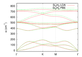
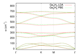
(II) The parameters in this model, as well as the justification for the choice of orbitals comes from first-principles studies using density functional theory (DFT) implemented in the vasp [20] plane-wave-basis code. First, we calculated the lattice parameters of silicane and germanane with multiple semilocal exchange-correlation functionals: the local density approximation (LDA) and the Perdew-Burke-Ernzerhof [21] (PBE) functionals. In addition the screened Heyd-Scuseria-Ernzerhof 06 (HSE06) functional [22] was used to obtain the electronic band structures to compensate (at least partially) for the underestimation of the band gap by semilocal functionals. The plane-wave cutoff energy was 500 eV. A Monkhorst-Pack k-point grid was used for geometry optimisations while a grid was used to calculate the band structures. The vertical separation of periodic images of the monolayer was set to 15 Å. The force tolerance in the optimisation was 0.005 eV/Å. Phonons were calculated with the force constant approach in a supercell.
We find that the relaxed structure of both silicane and germanane is very similar to that of graphane, as illustrated in Fig. 1. The parameters listed were obtained after a full geometry optimisation. The bond lengths obtained with the PBE functional are systematically larger than those optimised with the LDA, as expected [23]. Note that the hydrogenation is accompanied by a significant increase in the magnitude of the sublattice buckling when compared to silicene and germanene, where, according to LDA/PBE, Å and Å, respectively. Lattice constants and sublattice bucklings agree with previous literature within % and %, respectively [24, 25, 26, 27, 28].
The calculated electronic band structures are plotted in Fig. 2. In comparison to graphane [29] one important difference in silicane and germanane is that in the latter two materials a band appears close to the conduction band edge at the M point. While the conduction band minimum of Ge2H2 is at the point similar to C2H2, in the case of Si2H2 it is in fact at the M point, making silicane an indirect gap semiconductor. The band gaps of silicane and germanane are 2.91 eV and 1.90 eV, respectively, according to the HSE06 functional which is expected to underestimate the gap by no more than 10 % [30]. Note that the conduction band is anisotropic at the M point with a heavy effective mass in the direction. Our finding that the band gap of Si2H2 is indirect and that of Ge2H2 is direct is supported by previous literature using a variety of methods ranging from semi-local DFT through hybrid functionals to single-shot GW [24, 25, 27, 28].
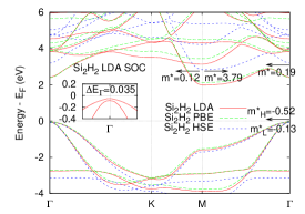
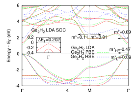
We have also looked at the effects of spin-orbit coupling. The insets in Fig. 2 show the spin-orbit induced splitting of the valence band at the point. The effect of spin-orbit coupling is more pronounced in the case of germanane where the valence band splits by an energy difference of 202 meV at .
Now we discuss the orbital composition of the valence and conduction bands of silicane and germanane (see Table 1). We find that at the point the valence band consists of Si/Ge and orbitals, while the conduction band is dominantly Si/Ge and . However, at the M point the conduction band also contains Si/Ge and contributions. The H orbital also contributes at the M point, to the valence band in silicane (and slightly to the conduction band in germanane). This means that for a tight-binding description of silicane and germanane an all valence description is required taking into account the , , , and orbitals of Si/Ge, as well as the H orbital.
| M | ||
|---|---|---|
| Si2H2 val. | ||
| Si2H2 cond. | ||
| Ge2H2 val. | ||
| Ge2H2 cond. |
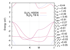
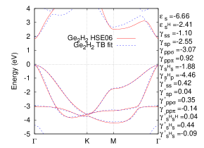
(III) We used the HSE06 band structures as reference to obtain the tight-binding parameters. We find that the tight-binding band structure can reproduce the entirety of the DFT valence band and the vicinity of the conduction band at both the and M points (see Fig. 3). It is important to note here that if we neglect second-nearest neighbour interactions the valence band can still be reproduced but the behaviour of the conduction band at the M point cannot, which indicates that the second nearest neighbour interactions are responsible for the minimum in the conduction band at the M point. Also, the -shell of Si/Ge is likely to affect states in the conduction band. The best fit is achieved with the parameters listed in the legend of Fig. 3; the fitting was optimised to give a quantitative description of the valence band and the conduction band near the and the M point.
(IV) Finally, we have performed a full geometry optimisation of Si2H2 and Ge2H2. While the geometry optimisation yields an energetically stable configuration for both materials, it is necessary to examine their phonon dispersions in order to ascertain whether they are dynamically stable. We find that silicane is stable as there is no sign of any dynamical instability anywhere along the high symmetry lines of the Brillouin zone (see Fig. 4). In the case of Ge2H2 we find a small pocket of instability for the flexural acoustic phonons. We believe that this is an artifact arising due to the difficulty in converging the flexural acoustic branch of two-dimensional materials as the phonon wave vector goes to zero. Since we find no other pockets of instability in any of the other branches we conclude that germanane is also dynamically stable. This is an important finding as the experiments in Ref. [18] were performed on multilayers of germanane on a substrate, while our calculations predict that suspended single-layer germanane would be stable, too.
It is worth noting that there is an alternate configuration for silicane and germanane not considered here. The so-called chair-like structure we studied corresponds to the case when H atoms alternate on the two sides of the sheet such that for each sublattice the H atom is on a fixed side. In the so-called boat configuration the H atoms alternate in pairs instead, which slightly increases the unit cell size. The latter has been shown to be notably less stable than the chair configuration in the case of graphane [29], nevertheless the boat configuration of silicane and germanane has been found to be stable [25] which is important to bear in mind.
In conclusion we have shown using first-principles density functional theory that freestanding hydrogenated silicene and germanene, better known as silicane and germanane, are energetically and dynamically stable. We have shown that silicane is an indirect and germanane a direct gap semiconductor and derived a tight binding model to describe the valence and conduction bands of these materials, fitting the parameters to hybrid density functional calculations. A minimum in the conduction band at the M point is caused by second nearest neighbour interaction which, in the case of silicane, leads to an indirect band gap.
References
References
- [1] K.S. Novoselov, A.K. Geim, S.V. Morozov, D. Jiang, Y. Zhang, S.V. Dubonos, I.V. Grigorieva, and A.A. Firsov, Science 306, 666 (2004).
- [2] A.K. Geim and K.S. Novoselov, Nature Materials 6, 183 (2007).
- [3] B. Aufray, A. Kara, S. Vizzini, H. Oughaddou, C. Léandri, B. Ealet, and G. L. Lay, Appl. Phys. Lett. 96, 183102 (2010).
- [4] P. E. Padova, C. Quaresima, C. Ottaviani, P. M. Sheverdyaeva, P. Moras, C. Carbone, D. Topwal, B. Olivieri, A. Kara, H. Oughaddou, B. Aufray, and G. L. Lay, Appl. Phys. Lett. 96, 261905 (2010).
- [5] B. Lalmi, H. Oughaddou, H. Enriquez, A. Kara, S. Vizzini, B. Ealet, and B. Aufray, Appl. Phys. Lett. 97, 223109 (2010).
- [6] N. D. Drummond, V. Zólyomi, and V. I. Fal’ko, Phys. Rev. B 85, 075423 (2012).
- [7] Y. Kubota, K. Watanabe, O. Tsuda, and T. Taniguchi, Science 317, 932 (2007)
- [8] M.P. Levendorf, C.-J. Kim,L. Brown, P.Y. Huang, R.W. Havener, D.A. Muller, and J. Park, Nature 488, 627 (2012).
- [9] K.F. Mak, C. Lee, J. Hone, J. Shan, and T.F. Heinz, Phys. Rev. Lett. 105, 136805 (2010).
- [10] B. Radisavljevic, A. Radenovic, J. Brivio, V. Giacometti, and A. Kis, Nature Nanotechnology 6, 147 (2011)
- [11] B. Radisavljevic, M.B. Whitwick, and A. Kis, ACS Nano 5, 9934 (2011).
- [12] T. Georgiou et al., Nature Nanotechnology 8, 100 (2013).
- [13] J.N. Coleman et al., Science 331, 568 (2011).
- [14] D. Braga, L.I. Gutiérrez, H. Berger, and A.F. Morpurgo, Nano Lett. 12, 5218 (2012).
- [15] C. Ataca, H. Sahin, and S. Ciraci, J. Phys. Chem. C 116, 8983 (2012).
- [16] V. Zólyomi, N. D. Drummond, and V. I. Fal’ko, Phys. Rev. B 87, 195403 (2013).
- [17] D. C. Elias, R. R. Nair, T. M. G. Mohiuddin, S. V. Morozov, P. Blake, M. P. Halsall, A. C. Ferrari, D. W. Boukhvalov, M. I. Katsnelson, A. K. Geim, and K. S. Novoselov, Science 323, 610 (2009).
- [18] E. Bianco, S. Butler, S. Jiang, O. D. Restrepo, W. Windl, and J. E. Goldberger, ACS Nano 7, 4414 (2013).
- [19] J. C. Slater and G. F. Koster, Physical Review 94, 1498 (1954).
- [20] G. Kresse and J. Furthmüller, Phys. Rev. B 54, 11169 (1996).
- [21] J. P. Perdew, K. Burke, and M. Ernzerhof, Phys. Rev. Lett. 77, 3865 (1996).
- [22] J. Heyd, G.E. Scuseria, and M. Ernzerhof, J. Chem. Phys. 118, 8207 (2003); A.V. Krukau, O.A. Vydrov, A.F. Izmaylov, and G.E. Scuseria, ibid. 125, 224106 (2006).
- [23] F. Favot and A. D. Corso, Phys. Rev. B 60, 11427 (1999).
- [24] L. C. Lew Yan Voon, E. Sandberg, R. S. Aga, and A. A. Farajian, Appl. Phys. Lett. 97, 163114 (2010).
- [25] M. Houssa, E. Scalise, K. Sankaran, G. Pourtois, V. V. Afanas’ev and A. Stesmans, Appl. Phys. Lett. 98, 223107 (2011).
- [26] J. C. Garcia, D. B. de Lima, L. V. C. Assali, and J. F. Justo, J. Phys. Chem. C 115, 13242 (2011).
- [27] O. Pulci, P. Gori, M. Marsili, V. Garbuio, R. Del Sole, and F. Bechstedt, Eur. Phys. Lett. 98, 37004 (2012).
- [28] W. Wei and T. Jacob, Phys. Rev. B 88, 045203 (2013).
- [29] J. O. Sofo, A. S. Chaudhari, and G. D. Barber, Phys. Rev. B 75, 153401 (2007).
- [30] S. Park, B. Lee, S. H. Jeon, and S. Han, Current Applied Physics 11, S337 (2011).
- [31] L. Liu and Z. Shen, Appl. Phys. Lett. 95, 252104 (2009).