Edge proximity-induced magnetoresistance and spin polarization in ferromagnetic gated bilayer graphene nanoribbon
Abstract
Coherent spin-dependent transport through a junction containing of Normal/Ferromagnetic/Normal bilayer graphene nanoribbon with zigzag edges is investigated by using Landauer formalism. In a more realistic set-up, the exchange field is induced by two ferromagnetic insulator strips deposited on the ribbon edges while a perpendicular electric field is applied by the top gated electrodes. Our results show that, for antiparallel configuration, a band gap is opened giving rise a semiconducting behavior, while for parallel configuration, the band structure has no band gap. As a result, a giant magnetoresistance is achievable by changing the alignment of induced magnetization. Application of a perpendicular electric field on the parallel configuration, results in a spin field-effect transistor where a fully spin polarization occurs around the Dirac point. To be comparable our results with the one for monolayer graphene, we demonstrate that the reflection symmetry and so the parity conservation fails in bilayer graphene nanoribbons with the zigzag edges.
pacs:
Spin polarization, magnetoresistance, ferromagnetic bilayer graphene, perpendicular applied gate voltageI Introduction
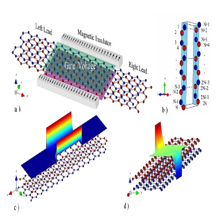
The recent successful fabrication of monolayer graphenenovoselov has been attracted great attention because it prepares appropriate building block for future nanoelectronics and spintronics. The Dirac Hamiltonian at low energy limit of graphene spectrum results in many peculiar properties, for instance, the half integer quantum Hall effectqhe , minimum conductivitymincond , the absence of back scatteringmincond ; back-scatter , Klein tunnelingklein . Furthermore, graphene has excellent transport properties such as long spin relaxation which makes it excellent candidate for spintronic devices. Because of weak spin orbit coupling, spin relaxation length of graphene can reach about one micron in dirty samples and room temperature tombros . Clean samples have longer spin coherency length. Carriers in graphene are not spin-polarized because graphene has not intrinsically ferromagnetism (FM) properties. However, FM can be induced extrinsically in graphene by doping defectsdefects , Coulomb interactionscoulomb or by applying an external electric field in the transverse direction in nanoribbonselectric . One of proposalsHaugen ; joza is the proximity effect of a FM insulator deposited on graphene sheet. Because of strong proximity, the wave functions of the localized magnetic states overlap with carriers in graphene sheet giving rise an induced exchange field in graphene. This induced exchange field which is tunable by application of an in-plane external electric field ex-tune induces a spin-polarized current in graphene. Using a ferromagnetic gate dielectric which is deposited on graphene layer as the channel, a spin field effect transistor has been proposed when spin manipulation is achievable by applying external perpendicular electric fieldsemenovAPL . External electric field can modify the exchange interaction.
The possibility of controlling spin conductance in monolayer graphene has also been recently studiedYokoyama . It was shown that because of induced exchange field and also due to the chiral resonant tunneling bound states inside the barrier, spin splitting of current emerges and has an oscillatory behavior in respect to the gate voltage and chemical potential. On the other hand, transport gap induced by the parity selection rule governing in the electronic bands of spectrum of zigzag graphene nanoribbons leads to large spin polarization and giant magnetoresistancezhang . Presence of the reflection symmetry in the incoming and outgoing wave functions of zigzag monolayer graphene nanoribbons leads to the parity selection rule which regulates the current flowcheraghchi . We will show in this paper that there is no such a symmetry and selection rule in bilayer graphene. Experimentally, possibility of fabrication graphene nanoribbons with ultra narrow widths and atomically smooth edges possibly well-defined zigzag or armchair-edge structures has been recently reportedDai . In zigzag graphene nanoribbons, spin current has been also predicted in presence of large electric fieldelectric . Large magnetoresistance (MR) also has been reported in monolayer graphene nanoribbonskim .
Much attention has been recently paid to bilayer graphene which consist of two parallel graphene sheets coupled each other with two sublattices and , in each layer. They are typically stacked in Bernal form as shown in Fig.1 leading to some interesting physical phenomena. For example new type of quantum Hall effectqhe-bilayer and also the energy band gap tunable by vertically applied electric field are of its peculiar properties in compared to monolayer graphene4band ; gap-BG ; gap-BG1 ; gap-BG2 . A meV band gap for bilayer graphene has been proposed by optical measurements and also theoretical predictions. Recently, an electrically tunable band gap has been observed in trilayer graphene with crystallographic stackingtrilayer . Controllable band gap introduces bilayer graphene as an excellent candidate for spintronic devicessemenov . The same as monolayer graphene, in the resonant bound states of the barrier, large spin polarization and also giant magnetoresistance has been reported in bilayer graphene in the limit of infinite widthnguyen ; Yu ; adineh . Motivated by the above mentioned studies we consider spin polarization and magnetoresistance in bilayer graphene nanoribbon with zigzag edges.
Mostly, FM insulator layers are deposited on top or bottom of BLG. However, simultaneous application of a perpendicular electric field which can be manipulated by means of the top-gate electrodes, affects the induced exchange field arising from a FM insulator layer. In this work, the exchange field is induced by the FM insulator strips deposited on the ribbon edges while a perpendicular electric field is applied by means of the top-gate electrodes. This structure is more realistic from the experimental point of view. So we have to deposit the gate electrodes separate of the FM insulator strips. A schematic cartoon of our considered system is shown in Fig.1 which contains the stacking of bilayer graphene nanoribbon accompanied with two strips of ferromagnetic insulator such as deposited on two edges of nanoribbon. The direction of magnetization of the strips can be essentially justified in the parallel or antiparallel configurations. The induced exchange field is directed to perpendicular of graphene sheet. To simulate more realistic situation, we suppose that the edge-induced magnetic potential exponentially decays from the edge toward the middle of nanoribbon. In the tight-binding model, we use Landauer-Buttiker formalism to calculate the spin-dependent conductance. We have found large spin polarization and magnetoresistance when a band gap is opened in the antiparallel configuration. The energy range in which spin polarization and magnetoresistance are large, can be extended by application of a perpendicular gate voltage. Based on this behavior, one can manipulate a spin filed effect transistor.
The paper is organized as the following sections: in section II, we introduce the model and Landauer-Buttiker formalism for calculating conductance. The numerical results and discussion about spin dependent conductance and spin filtering and also magnetoresistance are presented in section III. violation of parity conservation in bilayer graphene nanoribbons with even number of zigzag chains in width is presented in section IV. Finally a conclusion of contents is presented in section V.
II Hamiltonian and Formalism
We consider a bilayer graphene nanoribbon with Bernal stacking which is connected to the left and right electrodes as indicated in Fig.1. The total Hamiltonian, H, of the device can be divided into four parts as which are the Hamiltonian of the center region, the left and right electrodes, and also the coupling Hamiltonian, respectively. The electrodes are considered to be the same as the central portion. The model is the tight-binding nearest-neighboring approximation with one orbital per each site on the lattice. The effective Hamiltonian of bilayer graphene in the presence of magnetic strips is given as follows:
| (1) |
| (2) |
where and and and are creation and annihilation operators of an electron with spin in the sublattice in the layer at the th site respectively. The onsite energy is indicated by . Here, for . The interlayer nearest neighbor hopping energy is while the hopping energy between sublattices and in different layers is prependicular-hopping . The top and bottom gate voltages are applied through a uniform variation in onsite energies belonging to the topper () and lower () layers. As shown in Fig.1, FM strips deposited on the edges of nanoribbon induce the exchange field across BLG. The overlapping of the wave functions of the localized magnetic states existing in the FM strips with itinerant carriers of graphene reduces strongly with the distance. So it is reasonable to suppose an exponential decay for such overlapping with distance. For antiparallel configuration of FM strips, the induced magnetic potential exponentially decreases from the values of M and -M at the edges to zero in the middle of the ribbon. For parallel configuration, the induced magnetic potential reaches to its maximum value at the edges of nanoribbon as M and exponentially decays when one goes from the zigzag edges toward the middle of the ribbon..
The current flowing through the device can be calculated from the Landauer-Buttiker formula,
| (3) |
Where is the Fermi-Dirac distribution function of the left and right electrodes and is the transmission coefficient. In the transmission calculation, is the rate of escaping carriers from the central portion into the electrodes and is given by in which the related Green’s function is written as where is a positive infinitesimal number. Here is the retarded self-energy function emerging from semi-infinite electrodes. By calculating surface Green’s function nardelli and coupling Hamiltonian , one can calculate self-energies related to each electrode. After calculating the current, the conductance can be derived straightforwardly, , with the bias where is the chemical potential of electrodes. At zero temperature and linear regime, Datta .
III Numerical Results
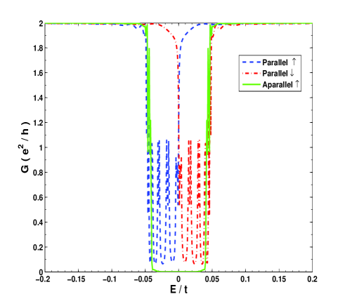
Conductance: Let us start describing transport mechanism for parallel and antiparallel configuration of magnetization of strips. Fig.2 shows conductance as a function of the Fermi energy for different configurations of FM strips. In the parallel (antiparallel) configuration, the exchange field inducing by FM insulators located on each edges are parallel (antiparallel) and exponentially reduces from the zigzag edges to the middle of the strip. Conductance for antiparallel configuration shows a transport gap around the Dirac point which is proportional to the spin splitting of the potential originating from the induced exchange field. In fact, those carriers with spin parallel to the induced exchange field (spin up) hits on the barrier whose magnetic potential is lower than the potential belonging to the spin down. For the parallel configuration of FM strips, depending on the type of spin, conductance oscillates with the amplitude about in an energy range which is equal to the potential splitting. This spin splitting of the potential barrier in the parallel configuration leads to a large spin polarization around the zero energy. By application of an electric field, one can control the direction of the exchange field inducing by FM strips. So based on this structure, observation of a large magnetoresistance around the Dirac point is potentially accessible when parallel configuration switches to antiparallel one by application of an electric field.
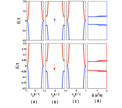
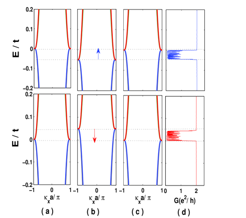
To understand the zero conductance plateau seen in the antiparallel configuration of FM strips, we plot the band structure of the left electrode, central portion and right electrode in Fig.3. In the antiparallel configuration, a band gap is opened in the band structure of the central portion around the zero energy. The band gap is originated from breaking of the chiral symmetry by application of an antiparallel exchange field on two edge sides of bilayer nanoribbon. So in the antiparallel configuration, system behaves as a semiconductor. However, there is no energy gap in the band structure of the parallel configuration. As shown in Fig.4, in the parallel configuration, spin-up (down) band structure of the central portion shifts to lower (higher) energies as much as the induced exchange potential. However, in the antiparallel configuration, the band structure is independent of spin type. Conductance in Fig.4 shows an oscillatory behavior which is concerned to resonant states arising from induced magnetic barrier shown in Fig.1-d. We also observed that the results are independent of even-odd effects of the number of zigzag chains in width.
Spin polarization: In the parallel configuration, spin splitting of conductance leads to large spin polarization around the zero energy. The spin polarization is defined as:
| (4) |
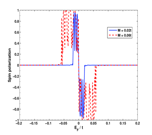
where and are conductance for up and down spins. Spin polarization in the parallel configuration is indicated in Fig.5 for different induced exchange potentials. In the energy range of , there is a filter of up spins, while in the energy range of , down spins are filtered. So the range of energies in which spin filter is observed increases with an increase of the induced exchange potential.
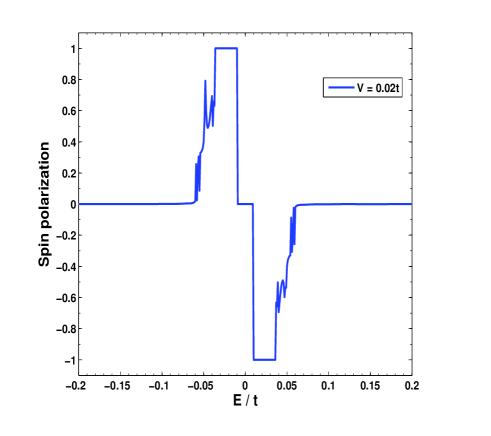
The advantage of bilayer graphene against monolayer is the existence of a controllable band gap which is produced by application of a perpendicular electric field. In the case of parallel configuration, Fig.6 indicates spin polarization through ZBGN with zigzag chains in width and unit cells in length in the presence of the external perpendicular electric field . Application of the potential difference () in the central region causes to emerge an energy gap which is equal to . So the first conduction and the last valance bands detach from each other so that they do not belong to the same band group. Therefore, as shown in Ref.cheraghchi-book, , transition between these subbands is not allowed now. It means that detaching of bands causes to block electron transition in the energy ranges of and . So two full spin polarized regions emerges by application of a vertically electric field in the parallel configuration. In these energy ranges, one of the spin types is fully blocked. Furthermore, the trace of energy band gap is seen in Fig.6 where spin polarization is zero around the zero energy.
Magnetoresistance: An in-plane electric field can change the exchange field direction inducing in graphene. So by switching between parallel and antiparallel configurations, a giant magnetoresistance is achievable. Magnetic resistance is defined as the following:
| (5) |
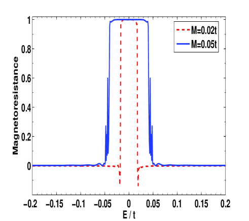
where and are conductance for parallel and antiparallel configurations. Fig.7 shows magnetoresistance as a function of Fermi energy. As we expect, magnetoresistance reaches to its maximum value in the energy window of . This large magnetoresistance is originated from the energy gap produced in the antiparallel case. Therefore such a system is a good candidate for spin valve devices.
In the last part of this work, let us have a comparison between the parity selection rules in monolayer and bilayer graphene nanoribbons. The parity conservation controls the electronic transport properties in zigzag monolayer graphene nanoribbonscheraghchi . It is interesting to check the validity of the parity conservation resulting from the reflection symmetry in bilayer graphene.
IV Violation of reflection symmetry in bilayer graphene nanoribbons
Attaching the second layer to the monolayer graphene causes to interact carbon atoms in the upper and lower layers with each other. The intera-layer hopping integral energy between carbon atoms located in different layers () is about times weaker than the inter-layer hopping energy (). However, nonzero results in the violation of the reflection symmetry in bilayer graphene nanoribbon when the number of zigzag chains is even. To check this violation, we calculate conductance through a step-like potential applied on ZBGN in which for , potential is zero and for , gated potential is . Here, is located in the junction between the left electrode and central region shown as in Fig.1. In this section, there is no applied perpendicular electric field nor FM strips. Fig.8 shows conductance through a step-like potential for even and odd ZBGN accompanied with the left and right band structures for different perpendicular hopping energies (). By application of the gate potential, band structures come out of the alignment such that the upper bands are aligned with the lower bands. It is interesting that if the connection between the upper and lower layers is disconnected (), parity conservation in even ZGNRs is the only selection rule which governs electronic transportcheraghchi in the energy window of . In this energy range and in the limit of two isolated monolayer graphene, states belonging to the left side of junction have opposite parity against states locating in the right side of the junction. Therefore as shown in Fig.8a, transport is blocked. However, if interaction between the upper and lower layers is gradually being turned on (), the reflection symmetry is gradually being violated and the electronic states located in the left side of the junction are able to scatter into the states located in the right side of the junction at the same energy. So conductance becomes nonzero in the energy window of .
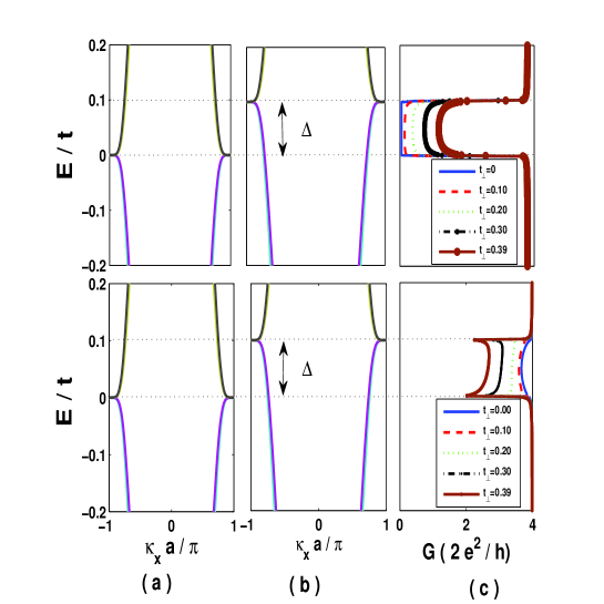
It is known that there is no reflection symmetry and thus parity conservation in odd monolayer ZGNRscheraghchi . So in the limit of two isolated graphene sheets (), as shown in Fig.8b, transmission is complete through the step-like potential in the energy window of [0,0.1]. By increasing interaction between two layers, intera-layer back-scattering causes to lower transmission. As a result, when hopping between atoms located in the upper and lower layers () reaches to its realistic value , Fig.8 indicates that there is no much difference in transport properties through even or odd ZGNRs.
V Conclusion
We study coherent spin dependent conductance through zigzag bilayer graphene nanoribbon (ZBGN) in the presence of two ferromagnetic insulator strips which are deposited on the edges of nanoribbon. This system sets as normal/ferromagnetic/normal graphene nanojunction. It is supposed that the induced exchange potential decreases exponentially when one goes from the edges into the middle of ribbon. Configuration of the exchange field inducing by the edge ferromagnetic insulators can be set as parallel or antiparallel with each other. A band gap is opened in bilayer graphene when the exchange fields arising from two ferromagnetic insulators are in the antiparallel situation. So in this case, ZBGN behaves as a semiconductor. However, in the parallel configuration of magnetization of strips, there is no gap. In the parallel configuration, conductance indicates spin polarized behavior around the zero energy. Spin polarization is intensified by application of a perpendicular electric field. On the other word, fully spin filter emerges in the energy ranges which are equal to the induced exchange field. In addition, a giant magnetoresistance is observed around the zero energy which is proportional to the induced exchange potential. To be comparable our results with the one for monolayer ZGNR, we demonstrate that the reflection symmetry and so the parity conservation fails in ZBGN.
VI Acknowledgement
All authors are grateful to Seyyed Ahmad Ketabi for useful discussions at the early stages of the work. H. CH. thanks the Condensed Matter Section of ICTP in Trieste for the hospitality and support during his visit to this institute.
References
- (1) K. S. Novoselov, A. K. Geim, S. V. Morozov, D. Jiang, Y. Zhang, S. V. Dubonos, I. V. Grigorieva, and A. A. Firsov, Science 306, 666 (2004).
- (2) Y. Zhang, Y. W. Tan, H. L. Stormer and P. Kim, Nature, 438 201 (2005); K. S. Novoselov, E. McCann, S. V. Morozov, V. I. Fal’ko, M. I. Katsnelson, U. Zeitler, D. Jiang, F. Schedin and A. K. Geim, Nat. Phys. 2, 177 (2006).
- (3) K. S. Novoselov, A. K. Geim, S. V. Morozov, D. Jiang, M. I. Katsnelson, I. V. Grigorieva, S. V. Dubonos, and A. A. Firsov, Nature (London) 438, 197 (2005); Nat. Phys. 2, 177 (2006); T. Ando, J. Phys. Soc. Japan 74, 777 (2005).
- (4) T. Ando, T. Nakanishi, J. Phys. Soc. Japan, 67, 1704 (1998); T. Ando, T. Nakanishi and R. Saito, J. Phys. Soc. Japan, 67, 2857 (1998).
- (5) M. I. Katsnelson, K. S. Novoselov, and A. K. Geim, Nat. Phys. 2, 620 (2006).
- (6) N. Tombros, C. Jozsa, M. Popinciuc, H. T. Jonkman, B. J. van. Wees, Nature, 448, 571 (2007).
- (7) O. V. Yazyev and L. Helm, Phys. Rev. B. 75, 125408 (2007); T. O. Wehling, K. S. Novoselov, S. V. Morozov, E. E. Vdovin, M. I. Katsnelson, A. K. Geim and A. I. Lichtenstein, Nano Lett. 8, 173, (2008); N. M. R. Peres, F. Guinea and A. H. Castro Neto, Phys. Rev. B. 72, 174406 (2005).
- (8) N. M. R. Peres, F. Guinea, and A. H. Castro Neto, Phys. Rev. B. 72, 174406 (2005).
- (9) Y. W. Son, M. L. Cohen and S. G. Louie, Nature, 444, 347 (2006).
- (10) H. Haugen, D. Huertas-Hernando, A. Brataas, Phys. Rev. B. 77, 115406 (2008).
- (11) C. Jozsa, M. Popinciuc, N. Tombros, H. T. Jonkman, and B. J. van Wees, Phys. Rev. Lett. 100, 236603 (2008).
- (12) E.-J. Kan, Z. Li, J. Yang and J. G. Hou, Appl. Phys. Lett. 91, 243116 (2007)); S. Dutta and S. K. Pati, J. Phys. Chem. B. 112, 1333 (2008).
- (13) Y. G. Semenov, K. W. Kim, J. M. Zavada, Appl. Phys. Lett. 91, 153105 (2007).
- (14) T. Yokoyama, Phys. Rev. B. 77, 073413 (2008).
- (15) Y. T. Zhang, H. Jiang and Q. f. Sun, X. C. Xie, Phys. Rev. B. 81, 165404 (2010).
- (16) H. Cheraghchi, H. Esmailzade, Nanotechnology, 21, 205306 (2010); H. Cheraghchi, Phys. Scr. 84, 015702 (2011).
- (17) X. Li, X. Wang, L. Zhang, S. Lee, H. Dai, Science, 319, 1229 (2008); X. Wang, Y. Ouyang, X. Li, H. Wang, J. Guo, H. Dai, Phys. Rev. Lett. 100, 206803 (2008).
- (18) W. Y. Kim and K. S. Kim, Nat. Nanotechnol. 3, 408 (2008͒).
- (19) K. S. Novoselov, et al., Nat. Phys. 2, 177 (2006).
- (20) T. Ohta, A. Bostwick, T. Seyller, K. Horn, and E. Rotenberg, Science 313, 951 (2006).
- (21) E. Castro, et. al., Phys. Rev. Lett. 99, 216802 (2007).
- (22) J. Oostinga, H. Heersche, X. Liu, A. Morpurgo, L. Vandersypen, Nat. Mater. 7, 151 (2008).
- (23) Y. Zhang, et. al, Nature, 459, 820 (2009).
- (24) C. H. Lui, Z. Li, K. Fai Mak, E. Cappelluti, T. F. Heinz, Nat. Physics, 7, 944–947 (2011).
- (25) Y. G. Semenov, J. M. Zavada, K. W. Kim, Phys. Rev. B. 77, 235415 (2008); Phys. Rev. Lett. 101, 147206 (2008).
- (26) V. Hung Nguyen, A. Bournel, P. Dollfus, J. Appl. Phys. 109, 073717 (2011).
- (27) Y. Yu, Q. Liang, J. Dong, Phys. Lett. A. 375, 2858 (2011).
- (28) H. Cheraghchi, F. Adinehvand, J. Phys. Condens. Matter. 24, 045303 (2012).
- (29) J. Nilsson, A. H. C. Neto, F. Guine, and N. M. R. Press, Phys.Rev.Lett. 97, 266801 (2006); Z. F. Wang, et all, Phys. Rev. B, 75, 085424 (2007).
- (30) M. B. Nardelli, Phys. Rev. B. 60, 7828 (1999).
- (31) S.Datta, Electronic Transport in Mesoscopic Systems (Cambridge U.P, Cambridge, 1995).see chapter 2 and references.
- (32) H. Cheraghchi,Graphene Simulation, (ISBN 978-953-308-60-2, Publisher: InTech, 2011) Chapter 7: Nonlinear Transport through Ultra Narrow Zigzag Graphene Nanoribbons.