Plasmon scattering from holes: from single hole scattering to Young’s experiment
Abstract
In this article, the scattering of surface plasmon polaritons (SPPs) into photons at holes is investigated. A local, electrically excited source of SPPs using a scanning tunnelling microscope (STM) produces an outgoing circular plasmon wave on a thick (200 nm) gold film on glass containing holes of 250, 500 and 1000 nm diameter. Fourier plane images of the photons from hole-scattered plasmons show that the larger the hole diameter, the more directional the scattered radiation. These results are confirmed by a model where the hole is considered as a distribution of horizontal dipoles whose relative amplitudes, directions, and phases depend linearly on the local SPP electric field. An SPP-Young’s experiment is also performed, where the STM-excited SPP-wave is incident on a pair of 1 m diameter holes in the thick gold film. The visibility of the resulting fringes in the Fourier plane is analyzed to show that the polarization of the electric field is maintained when SPPs scatter into photons. From this SPP-Young’s experiment, an upper bound of 200 nm for the radius of this STM-excited source of surface plasmon polaritons is determined.
pacs:
07.79.Cz, 42.25.Fx,42.25.Hz,73.20.Mf1 Introduction
Surface plasmon polaritons (SPPs) are intensely studied for their use in potential nanophotonic applications as their electromagnetic fields can be confined to dimensions much smaller than the wavelength of light[1]. SPPs are a key element in the extraordinary optical transmission (EOT) of light[2] through arrays of holes of subwavelength diameter in opaque metal films, a phenomenon which has generated much excitement and fundamental and applied research[3, 4]. Despite this intense activity, an understanding of the scattering of SPPs into photons at holes remains incomplete.
In order to understand the scattering of plasmons into photons at holes and better understand EOT, a well-controlled experiment is necessary. In such an experiment, surface plasmon polaritons must be excited on the sample away from the hole, and the plasmons must have the opportunity to propagate to and interact with the hole. An experiment using this geometry has recently been reported[5] in which the authors focused on the scattering of an SPP plane wave from a single subwavelength hole into forward and radial plasmon waves. To our knowledge, however, an extensive study on the SPP scattering from a single subwavelength hole into photons has not been realized before our work. Single holes have also been investigated by directly exciting the hole and measuring the transmitted light in the far field[6, 7, 8], in the near-field[9, 10, 11] or using a leakage radiation microscope[12]. A scanning near-field microscope (SNOM) tip in illumination mode has also been used to investigate single subwavelength holes[13, 14]. However, the spatial and angular distribution of the light scattered from SPPs at single holes, has not been studied until now.
Young’s experiment—the observation of an interference pattern when an opaque screen perforated by two holes is placed before a light source—has been investigated under various different forms involving plasmons[14, 15, 16, 17, 18, 19, 20, 21, 22, 23, 24, 25, 26, 27]. In particular, an “all SPP” version has been demonstrated where the “holes” are replaced by two metal stripe waveguides[15]. Hole pairs have also been optically excited simultaneously[17, 18], as well as individually[19, 20], demonstrating the existence of plasmon propagation between slits in such experiments[18, 19, 20, 21]. The light scattered from the ends of a locally excited nanowire may also be considered a type of Young’s experiment[28, 29]. Again, however, the interference between the light scattered at two holes from propagating surface plasmons has never been previously examined. Such an experiment is important as it provides a method for studying the coherence of SPPs.
In this article, we investigate the scattering of surface plasmon polaritons into photons at single and double holes on a 200 nm-thick gold film. These SPPs are excited electrically and locally with a scanning tunnelling microscope (STM), producing an outgoing circular plasmon wave[30, 31]. This local excitation, the ability to precisely position the excitation source and the absence of any background light from the excitation are essential for these experiments. For the single hole experiment, diameters of 250, 500 and 1000 nm are considered. The scattered light at the holes is seen to be directional along the tip-hole axis and this directionality increases with hole diameter. For the double hole case, we see that the visibility of the resulting interference pattern varies as a result of excitation position due to the polarization of the STM-excited plasmons. Simulations where the hole scattering is considered as a series of in-plane coherent dipoles are in good agreement with the experimental results. This work demonstrates a novel method for studying the coherence properties of surface plasmon polaritons and allows us to estimate an upper bound for the size of the excitation source.
2 Experimental methods
The sample used consists of a 200 nm-thick (i.e., opaque) gold film deposited on glass. Widely spaced single and pairs of holes with diameters of 250, 500 and 1000 nm are etched in the film by focused ion beam lithography. The SPP-excitation on the gold film is carried out using an ambient STM coupled to an inverted optical microscope equipped with a x100 oil immersion objective (numerical aperture NA)[30, 32]. Photons produced by the scattering of SPPs at the single holes and at the hole pairs are collected below the sample and focused onto a cooled charge-coupled device (CCD) camera. An extra lens may be added in order to image the Fourier plane on the CCD camera. The collected light may also be analyzed with a spectrometer. For all real space and Fourier space images shown in the following, the STM parameters are = 6 nA, = 2.8 V and the integration time of the CCD camera is 60 s. The STM tip used is made of electrochemically etched tungsten.
3 Single hole scattering
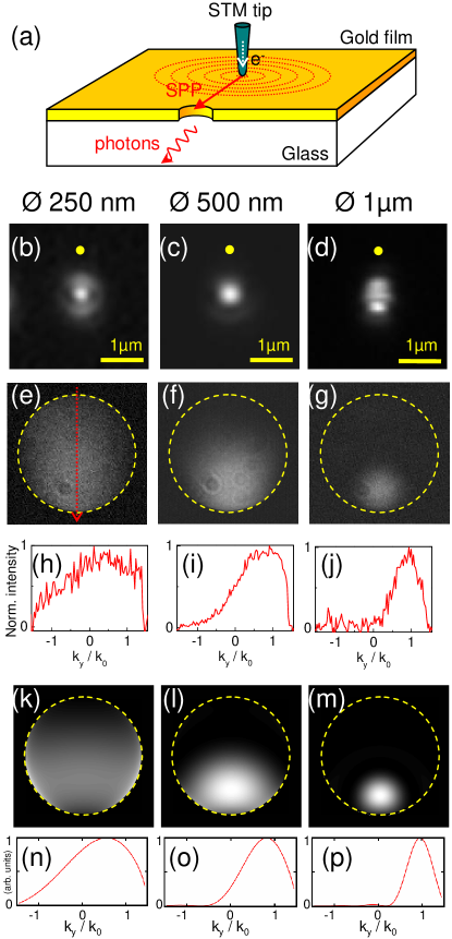
Figure 1(a) shows the principle of the single hole experiment. The STM tip excites a circularly propagating plasmon wave (on the gold-air interface) which upon reaching the hole is scattered into photons. Figures 1(b)-(d) show the real plane images obtained during such an experiment for three holes of different diameter. In each case the STM tip excitation position is denoted by the yellow dot in the figure.
The real space image varies as a function of hole diameter. For the subwavelength 250 nm hole, the real space image consists of three bright spots aligned along the tip-hole axis, with the brightest spot centered on the hole. This is reminiscent of a horizontal dipole above a glass substrate[33]. The result for the 500 nm hole consists of a single bright spot centered on the hole and the largest (1 m) diameter again gives rise to a three spot pattern along the tip-hole axis. This time the brightest spot is the one that is farthest from the tip excitation position. Note that this result is reminiscent of the prolate shape observed in [14] whose orientation depends on the polarization of the SNOM excitation light.
Figures 1(e)-(g) and the vertical cross-sections (h)-(j) show the corresponding Fourier plane images for the single hole experiments. The differences due to hole diameter are even more remarkable in the Fourier plane. A slight asymmetry is observed for the Fourier plane image of the 250 nm hole with a symmetry axis along the tip-hole direction. This asymmetry becomes more and more pronounced as the size of the hole increases, with the radiation clearly forward-peaked near the air/glass critical angle for the largest sized hole (1 m).
Figure 1(k)-(q) shows the simulation results of Fourier plane images for the three different hole diameters. A hole is modelled as a distribution of horizontal dipoles whose relative amplitudes, directions, and phases at a point in the plane depend linearly on the local SPP in-plane electric field of the incoming SPP plane wave at the same location. We have where the polarizability is chosen constant for simplicity. The radiation field imaged in the Fourier plane of the high NA objective is calculated by using the exact Green dyadic propagator for the electromagnetic field in the non-paraxial regime[34, 35, 36, 37], and by summing over the dipole distribution in the hole. See the Appendix A for further details. As in the case of the experimental data, the emitted radiation becomes strongly peaked in the forward direction as the hole diameter increases. This may be understood as a diffraction/interference phenomenon in which the emitted radiation interferes constructively in the forward direction and destructively otherwise. Thus we may consider the scattering of plasmons from holes analogous to the scattering of light by particles, where the object’s response to an optical excitation is considered multipolar, and retardation effects are taken into account. It is these resulting phase differences which give rise to the directivity of the scattered light.
4 Double hole scattering: Young’s experiment
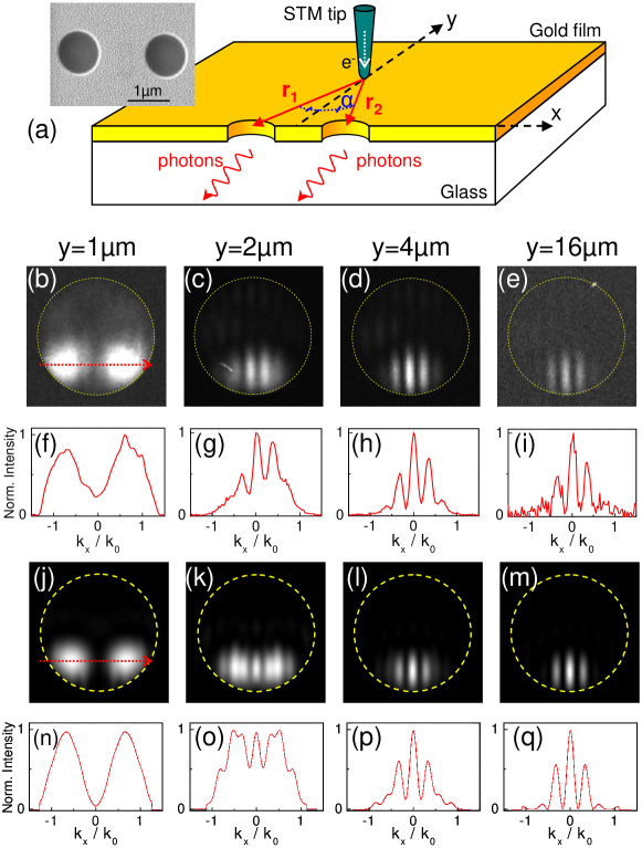
In the next experiment a pair of 1 m-diameter holes separated by 2 m is used. In figure 2(a) the principle of the experiment is explained and a scanning electron microscope image of the hole pair is displayed. The STM tip is positioned along the -axis (i.e., the perpendicular bisector of the line joining the two holes) and a circular plasmon wave is excited on the Au film with the STM. The SPP wavefronts travel a distance to the holes before being scattered into the far field. As in Young’s double slit experiment, an interference fringe pattern will be observed in the Fourier plane if there is a fixed phase difference between the radiation from the two holes.
From these experiments we gain information on the plasmon source size, polarization and coherence. Figure 2(b)-(i) shows Fourier plane images and the corresponding cross-sections of the resulting fringes when the STM tip is used to excite SPPs at different positions along the perpendicular bisector of the line joining the two holes. As the tip is moved away from the two holes, a dramatic increase in the contrast or visibility is initially observed. The visibility then stabilizes near a value of 1 for tip positions even further away on the -axis. The visibility is defined as
| (1) |
where and are the intensities corresponding the maximum and adjacent minimum of the fringes[38].
The low value of the fringe visibility for tip positions close to the hole pair may be understood by considering the polarization of the excited plasmons. As a first approximation we consider the two holes as point sources whose in-plane electric fields are in the direction of SPP propagation (i.e., and , see figure 2(a)). Thus we have
| (2) |
where and are the amplitude and phase respectively of the two point sources. When these two sources interfere in the Fourier plane we get
| (3) |
where is the distance between the two holes and is the coordinate in the Fourier plane (i.e., the in-plane component of the wave vector of the emitted radiation. is the photon wavelength in free space and is the index of refraction and is the angle with respect to the optical axis). Thus, after averaging over a finite interval longer than the coherence time and taking into account the correlations between the optical disturbances at each hole we obtain
| (4) |
with
| (5) | |||
| (6) |
where is the complex degree of coherence[39], and is related to the ability of the light from the two holes to form interference fringes. and are the respective intensities at each hole. is a time interval equal to the path difference between the source and the two holes divided by the velocity. With the same plasmon wavefront arriving at the two holes at the same time (see figure 2(a)) we have and . The term is the result of the in-plane polarization of the source plasmons.
From the definition of the visibility (equation 1) and the above (equation 4) and taking since the holes are equidistant from the source we obtain
| (7) |
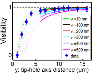
Thus when the holes are 2 m apart (=1 m) and the excitation point is 1 m away from the hole axis (m) and the visibility falls to zero. This is confirmed in figure 2(b) and (f) where no fringes are seen. It should be noted that while there is less and less overlap between the scattered light from the two holes as the tip is brought closer to them due to the directionality of the scattering, it is the polarization of the scattered light that causes the lack of interference fringes. On the other hand, when the tip is comparatively far from the holes as in figure 2(e) and (i) (m), and the visibility is maximal. This evolution of the visibility with the tip excitation position is shown in more detail in figure 3 (blue data points). These results clearly show that the light scattered at the two holes maintains the initial polarization of the incident plasmon wave.
Figure 2(j)-(m) shows the simulation results for the hole pair experiments. Again the calculations agree well with the experimental data. The small discrepancies at large angle (i.e. large , ) between the data and our model are possibly due to geometrical aberrations in the objective that are not taken into account in the simulation. Another source of error may be that no hole-reflected SPP wave is taken into account.
Not only do these experimental results tell us about the source polarization, but also about the source size. If we approximate the source seen by the two holes as a disc and use the van Cittert-Zernike theorem[38, 39] we can determine the degree of coherence at the two holes[40]. This formalism is only valid when both the source and hole separation are small compared to the tip-hole distance. Once these conditions are satisfied, the degree of coherence is equal to the absolute value of the normalized Fourier transform of the intensity function of the source, or more explicitly for a circular source :
| (8) |
is the radius of the circular source, is the distance between the two holes, is the wavelength and is the perpendicular distance from the source to the hole axis. Of these variables, only the size of the source is unknown. Thus from the data we can first determine the visibility (via equation 1) then find the degree of coherence from equation 7 and finally estimate an upper bound for the source size from equation 8. In figure 3, we have plotted the visibility for different values of the source radius and find a best fit to the data for the case where nm. Note that all the curves for nm pass through the error bars of the data so that this is indeed only an upper bound for the effective source size. The error introduced by the fact that the source is not strictly monochromatic may be shown to be on the order of 2% (see Appendix B). If the STM tip excitation position is no longer restricted to the -axis (i.e., the perpendicular bisector of the hole axis), then the plasmon path difference for the source to each of the two holes is no longer zero and . In such an experiment, may be determined and the temporal coherence of the STM-excited surface plasmons investigated.
5 Conclusion
In conclusion we have shown that the radiation from STM-excited SPPs scattered at holes becomes more and more directional as the hole size increases. This effect has been reproduced using a dipolar model. An SPP-Young’s experiment has been performed and the visibility as a function of the excitation position investigated, demonstrating that the polarization is maintained when SPPs are scattered into photons at holes. From this visibility data, an upper bound of 200 nm on the SPP source size has been determined. Such a small, electrically-excited SPP source that generates no background excitation radiation is a unique tool for the study of SPP coherence, and quantum SPP properties such as wave particle duality and SPP coupling to quantum emitters[28, 41, 42, 43].
Appendix A: Model
In our model we consider a cylindrical hole of radius and height
in a metal film with permittivity
. The mathematical approach consists
of removing a cylinder of metal from the film of thickness
and replacing it with an identical cylinder filled with air (i.e., with
permittivity
).
The electric displacement field
at point in the region surrounding each hole is
given by a Lippman Schwinger integral
where is the total dyadic
Green tensor corresponding to the film without a hole, the integration
volume corresponds to the cylindrical region occupied by the
hole (filled with air) and is the
incident SPP field propagating along the interface and existing
without the hole. In the transmitted region (i.e., in the substrate),
and only the volume integral
survives. Now, to a first-order (Born) approximation, we can write in
the transmitted region ,
where is the incident unperturbed SPP
field. However, since the SPP field strongly decays in the metal
(penetration length ) the volume integral
evolves into a surface integral over the aperture area :
,
where the coefficient arises from the integration of
the SPP exponential decay in the metal. We point out that it is
mainly the in-plane field which contributes to the signal since in
the metal .
Finally, in the far-field the propagation through the microscope can
be taken into account by modifying the dyadic Green function. In the
Fourier plane of the objective the signal field is therefore to a
first approximation proportional to the structure factor defined by
| (9) |
which is calculated for the in-plane wave vector ( is the oil index, and are the angle of photon emission in the spherical coordinate system with symmetry axis ). In our model we also take into account the modification of this formula using the formalism developed by Tang et al.[36] for large numerical aperture microscope objectives. The dependence of the results on wavelength is found to be weak in the wavelength range of interest. Consequently, the calculations used the peak wavelength of the measured spectrum.
Appendix B: Spectrum
The error introduced by the fact that the source is not strictly monochromatic may be shown to be on the order of 2%. The coherence length of a source may be determined from its spectral bandwidth via the expression[44]
| (10) |
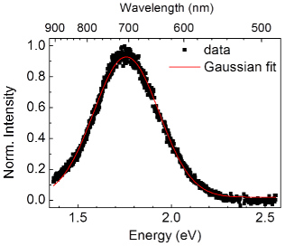
where is the plasmon wave velocity. From a spectral measurement of the light scattered by a pair of 1 m diameter holes (see figure 4) we obtain a value of 2 m for . Similarly, the degree of coherence as a function of path difference is given by the expression[44]
| (11) |
Using the value of found from the measured spectrum and nm for the (maximum) path difference we obtain (compared to a value of 1 that would be obtained with a strictly mono-chromatic source with infinite coherence length). From equation 7 in the main text we see that the resulting error on the visibility will be at most on the order of 2%.
References
References
- [1] W. L. Barnes, A. Dereux, and T. W. Ebbesen. Surface plasmon subwavelength optics. Nature, 424(6950):824–830, 2003.
- [2] T. W. Ebbesen, H. J. Lezec, H. F. Ghaemi, T. Thio, and P. A. Wolff. Extraordinary optical transmission through sub-wavelength hole arrays. Nature, 391(6668):667–669, February 1998.
- [3] C. Genet and T. W. Ebbesen. Light in tiny holes. Nature, 445(7123):39–46, January 2007.
- [4] F. J. Garcia-Vidal, L. Martin-Moreno, T. W. Ebbesen, and L. Kuipers. Light passing through subwavelength apertures. Rev. Mod. Phys., 82(1):729–787, January 2010.
- [5] N. Rotenberg, M. Spasenovic, T. L. Krijger, B. le Feber, F. J. Garcia de Abajo, and L. Kuipers. Plasmon scattering from single subwavelength holes. Phys. Rev. Lett., 108(12):127402, March 2012.
- [6] J. Prikulis, P. Hanarp, L. Olofsson, D. Sutherland, and M. Kall. Optical spectroscopy of nanometric holes in thin gold films. Nano Lett., 4(6):1003–1007, June 2004.
- [7] Y. Alaverdyan, B. Sepulveda, L. Eurenius, E. Olsson, and M. Kall. Optical antennas based on coupled nanoholes in thin metal films. Nat. Phys., 3(12):884–889, December 2007.
- [8] J. . M. Yi, A. Cuche, F. de Leon-Perez, A. Degiron, E. Laux, E. Devaux, C. Genet, J. Alegret, L. Martin-Moreno, and T. W. Ebbesen. Diffraction regimes of single holes. Phys. Rev. Lett., 109(2):023901, July 2012.
- [9] L. Yin, V. K. Vlasko-Vlasov, A. Rydh, J. Pearson, U. Welp, S. H. Chang, S. K. Gray, G. C. Schatz, D. B. Brown, and C. W. Kimball. Surface plasmons at single nanoholes in au films. Appl. Phys. Lett., 85(3):467–469, July 2004.
- [10] S. H. Chang, S. K. Gray, and G. C. Schatz. Surface plasmon generation and light transmission by isolated nanoholes and arrays of nanoholes in thin metal films. Opt. Express, 13(8):3150–3165, April 2005.
- [11] Tomas Rindzevicius, Yury Alaverdyan, Borja Sepulveda, Tavakol Pakizeh, Mikael Kall, Rainer Hillenbrand, Javier Aizpurua, and F. Javier Garcia de Abajo. Nanohole plasmons in optically thin gold films. J. of Phys. Chem. C, 111(3):1207–1212, January 2007.
- [12] Anne-Laure Baudrion, Fernando de Leon-Perez, Oussama Mahboub, Andreas Hohenau, Harald Ditlbacher, Francisco J. Garcia-Vidal, Jose Dintinger, Thomas W. Ebbesen, Luis Martin-Moreno, and Joachim R. Krenn. Coupling efficiency of light to surface plasmon polariton for single subwavelength holes in a gold film. Opt. Express, 16(5):3420–3429, March 2008.
- [13] M. Brun, A. Drezet, H. Mariette, N. Chevalier, J. C. Woehl, and S. Huant. Remote optical addressing of single nano-objects. Europhys. Lett., 64(5):634–640, December 2003.
- [14] C. Sonnichsen, A. C. Duch, G. Steininger, M. Koch, G. von Plessen, and J. Feldmann. Launching surface plasmons into nanoholes in metal films. Appl. Phys. Lett., 76(2):140–142, January 2000.
- [15] Rashid Zia and Mark L. Brongersma. Surface plasmon polariton analogue to young’s double-slit experiment. Nature Nanotech., 2(7):426–429, July 2007.
- [16] Marianne Derouard, Jerome Hazart, Gilles Lerondel, Renaud Bachelot, Pierre-Michel Adam, and Pascal Royer. Polarization-sensitive printing of surface plasmon interferences. Optics Express, 15(7):4238–4246, April 2007.
- [17] V. Haefele, F. de Leon-Perez, A. Hohenau, L. Martin-Moreno, H. Plank, J. R. Krenn, and A. Leitner. Interference of surface plasmon polaritons excited at hole pairs in thin gold films. Appl. Phys. Lett., 101(20):201102, November 2012.
- [18] H. F. Schouten, N. Kuzmin, G. Dubois, T. D. Visser, G. Gbur, P. F. A. Alkemade, H. Blok, G. W. Hooft, D. Lenstra, and E. R. Eliel. Plasmon-assisted two-slit transmission: Young’s experiment revisited. Phys. Rev. Lett., 94(5):053901, February 2005.
- [19] N. Kuzmin, G. W. T. Hooft, E. R. Eliel, G. Gbur, H. F. Schouten, and T. D. Visser. Enhancement of spatial coherence by surface plasmons. Opt. Lett., 32(5):445–447, March 2007.
- [20] S. Ravets, J. C. Rodier, B. Ea Kim, J. P. Hugonin, L. Jacubowiez, and P. Lalanne. Surface plasmons in the young slit doublet experiment. Journal of the Optical Society of America B-optical Physics, 26(12):B28–B33, December 2009.
- [21] P. Lalanne, J. P. Hugonin, and J. C. Rodier. Theory of surface plasmon generation at nanoslit apertures. Phys. Rev. Lett., 95(26):263902, December 2005.
- [22] L. Aigouy, P. Lalanne, J. P. Hugonin, G. Julie, V. Mathet, and M. Mortier. Near-field analysis of surface waves launched at nanoslit apertures. Phys. Rev. Lett., 98(15):153902, April 2007.
- [23] Choon How Gan, Greg Gbur, and Taco D. Visser. Surface plasmons modulate the spatial coherence of light in young’s interference experiment. Phys. Rev. Lett., 98(4):043908, January 2007.
- [24] Domenico Pacifici, Henri J. Lezec, Luke A. Sweatlock, Robert J. Walters, and Harry A. Atwater. Universal optical transmission features in periodic and quasiperiodic hole arrays. Opt. Express, 16(12):9222–9238, June 2008.
- [25] D. Pacifici, H. J. Lezec, Harry A. Atwater, and J. Weiner. Quantitative determination of optical transmission through subwavelength slit arrays in ag films: Role of surface wave interference and local coupling between adjacent slits. Phys. Rev. B, 77(11):115411, March 2008.
- [26] S. Aberra Guebrou, J. Laverdant, C. Symonds, S. Vignoli, and J. Bellessa. Spatial coherence properties of surface plasmon investigated by young’s slit experiment. Opt. Lett., 37(11):2139–2141, June 2012.
- [27] S. Aberra Guebrou, J. Laverdant, C. Symonds, S. Vignoli, F. Bessueille, and J. Bellessa. Influence of surface plasmon propagation on leakage radiation microscopy imaging. Appl. Phys. Lett., 101(12):123106, September 2012.
- [28] Roman Kolesov, Bernhard Grotz, Gopalakrishnan Balasubramanian, Rainer J. Stoehr, Aurelien A. L. Nicolet, Philip R. Hemmer, Fedor Jelezko, and Joerg Wrachtrup. Wave-particle duality of single surface plasmon polaritons. Nat. Phys., 5(7):470–474, July 2009.
- [29] Yang Zhang, Elizabeth Boer-Duchemin, Tao Wang, Benoit Rogez, Genevieve Comtet, Eric Le Moal, Gerald Dujardin, Andreas Hohenau, Christian Gruber, and Joachim R. Krenn. Edge scattering of surface plasmons excited by scanning tunneling microscopy. Opt. Express, 21(12):13938–48, June 2013.
- [30] T. Wang, E. Boer-Duchemin, Y. Zhang, G. Comtet, and G. Dujardin. Excitation of propagating surface plasmons with a scanning tunnelling microscope. Nanotechnology, 22(17):175201, April 2011.
- [31] Palash Bharadwaj, Alexandre Bouhelier, and Lukas Novotny. Electrical excitation of surface plasmons. Physical Review Letters, 106(22):226802, June 2011.
- [32] Eric Le Moal, Sylvie Marguet, Benoit Rogez, Samik Mukherjee, Philippe Dos Santos, Elizabeth Boer-Duchemin, Genevieve Comtet, and Gerald Dujardin. An electrically excited nanoscale light source with active angular control of the emitted light. Nano Letters, 13(9):4198–205, September 2013.
- [33] B. Sick, B. Hecht, and L. Novotny. Orientational imaging of single molecules by annular illumination. Phys. Rev. Lett., 85(21):4482–4485, November 2000.
- [34] M. Paulus, P. Cay-Balmaz, and O. J. F. Martin. Accurate and efficient computation of the green’s tensor for stratified media. Phys. Rev. E, 62(4):5797–5807, October 2000.
- [35] Lukas Novotny and Bert Hecht. Principles of nano-optics. Cambridge University Press, 2006.
- [36] Wai Teng Tang, Euiheon Chung, Yang-Hyo Kim, Peter T. C. So, and Colin J. R. Sheppard. Investigation of the point spread function of surface plasmon-coupled emission microscopy. Opt. Express, 15(8):4634–4646, April 2007.
- [37] A. Hohenau, J. R. Krenn, A. Drezet, O. Mollet, S. Huant, C. Genet, B. Stein, and T. W. Ebbesen. Surface plasmon leakage radiation microscopy at the diffraction limit. Opt. Express, 19:25749–25762, 2011.
- [38] Eugene Hecht. Optics. Addison-Wesley, 1990.
- [39] Max Born and Emil Wolf. Principles of Optics. Cambridge University Press, 7th edition edition, 1999.
- [40] B. J. Thompson and E. Wolf. Two-beam interference with partially coherent light. J. Opt. Soc. Am., 47:895, 1957.
- [41] A. Cuche, O. Mollet, A. Drezet, and S. Huant. ”deterministic” quantum plasmonics. Nano Letters, 10(11):4566–4570, 2010.
- [42] Oriane Mollet, Serge Huant, Geraldine Dantelle, Thierry Gacoin, and Aurelien Drezet. Quantum plasmonics: Second-order coherence of surface plasmons launched by quantum emitters into a metallic film. Phys. Rev. B, 86(4):045401, July 2012.
- [43] M. S. Tame, K. R. McEnery, S. K. Oezdemir, J. Lee, S. A. Maier, and M. S. Kim. Quantum plasmonics. Nat. Phys., 9(6):329–340, June 2013.
- [44] J. W. Goodman. Statistical Optics. Wiley, 1985.