Random Telegraph Signal in a Metallic Double-Dot System
Abstract
In this work we investigate the dynamics of a single electron surface trap, embedded in a self-assembly metallic double-dot system. The charging and discharging of the trap by a single electron is manifested as a random telegraph signal of the current through the double-dot device. We find that we can control the duration time that an electron resides in the trap through the current that flows in the device, between fractions of a second to more than an hour. We suggest that the observed switching is the electrical manifestation of the optical blinking phenomenon, commonly observed in semiconductor quantum dots.
Keywords: Random telegraph signal; Double dot; Metallic nanoparticles; Self-assembly; Charge trap; Photoluminescence blinking; Electrical transport;
Double quantum dot systems offer a unique opportunity for studying the world of quantum transport 1, and are considered promising candidates for quantum information operations 2. This stems from the ability to localize an electron in a limited region in space on the dot, and monitor its presence and properties, through the rich Coulomb blockade behavior 3, 4, 5. This concept has been realized in a variety of material systems with controlled size and shape, down to a few nanometers scale 6, 7, 8, 9, 10, 11. Another system, in which electrons can be stored and measured, is an electronic trap in solid 12, 13, 14. The electrons in such a trap are better isolated from the environment. However, their measurement and control are more difficult.
Here we demonstrate how these two systems, metallic double-dots and electronic traps, are combined to yield a hybrid structure in which an electron can be stored for long durations and can be easily detected and measured. The charging and discharging of the trap by a single electron is manifested as a Random Telegraph Signal (RTS) of the current through the double-dot device. RTS was studied in other systems of nano-objects, including semiconductor nanorods 15 and dots 16, and molecular junctions 17. It is commonly attributed to charging and discharging of surface traps, or to reconfiguration of molecular charge states. Here we study RTS in a self-assembled metallic nanoparticle double-dot system. We show that we can control the duration that an electron resides in the trap through the current, varying it between fractions of a second to minutes. Furthermore, we show that at the Coulomb blockade region, when no current is flowing, the electron can be kept in the trap for extremely long times ( hour). We find significant similarities between the electrical RTS in the metallic nanoparticle system and the optical blinking observed in semiconductor quantum dots 18, 19, suggesting that these are the optical and electrical manifestation of the same phenomenon.
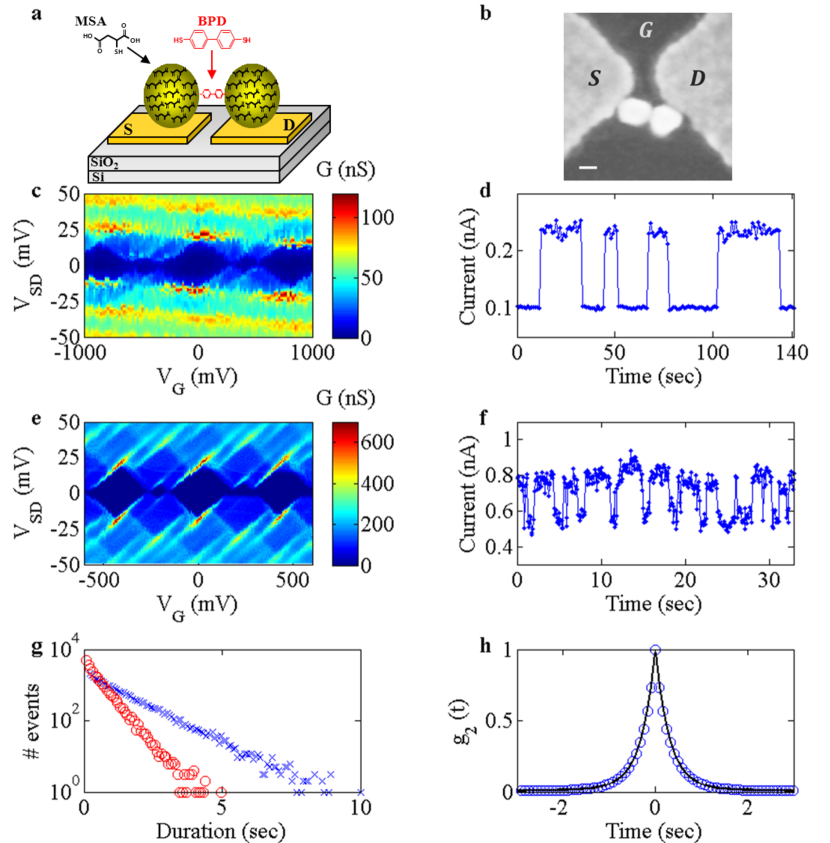
The system consists of two metallic nanoparticles (NPs) on top of a Si/SiO2 substrate [Fig. 1(a)-(b)]. The NPs are Au nm spheres, covered by a dense capping layer of mercaptosuccinic acid that acts as a tunnel barrier for electrical current into and from the NP. The dimer is formed by covalently linking the spheres with a short organic molecule, 4,4’-biphenyldithiol (BPD), thus forming a sub-nanometer gap between them 20, 11, and placed between e-beam defined electrodes by means of electrostatic trapping \bibnotemark[2]. The Si substrate is n-doped and used as a back gate. The measurements were done in a dilution refrigerator at a temperature of mK.
Typical electrical conductance properties as a function of the back gate voltage, , and the source-drain voltage, , are shown in Fig. 1(c),(e). The Coulomb blockade regime, consisting of a series of low conductance regions (diamonds) near zero is clearly visible. The large diamonds correspond to charging an extra electron on one of the dots, and the small ones - to charging the second dot while the first dot is already charged.
A noisy behavior is readily observed throughout the plane of device A [Fig. 1(c)]. We find that it corresponds to a time dependent switching behavior: Figure 1(d) shows a measurement of the current for over sec. The current abruptly switches between nA to nA, and remains at each conductance state (”on” and ”off”) for time durations and , which may vary in length. Such switching behavior, commonly known as random telegraph signal, is found in almost all devices we studied, each with different contrast and time durations. This ”noisy” pattern is the focus of our study.
Figures 1(e)-(f) show similar measurements of another device (device B), in which the conductance contrast is smaller and the time durations are substantially shorter. The fast dynamics of this device allows us to follow and analyze its behavior over many switching events. Figure 1(g) shows a histogram of that represents more than switching events. Clear exponential distributions are seen, from which the characteristic lifetime of these states, , can be extracted. Such exponential distributions are found in all measured devices.
The significance of these well-defined lifetimes can be realized by examining the time auto-correlation function of the measured RTS,
| (1) |
where , and represents time average. We find that this function falls exponentially at a decay rate which is the sum of the two inverse lifetimes, [Fig. 1(h)]. This behavior provides a useful insight into the underlying mechanism of RTS, as it describes a trap that is fed by an electron at a rate and is emptied at . One can describe the rate equations for its occupation probabilities as:
| (2a) | |||||
| (2b) | |||||
where . Solving equations (2) we indeed get . We, therefore, conclude that a trapped electron gates the double dot system and modifies its electrical conductance: different current levels correspond to different states of the trap - either empty or occupied.
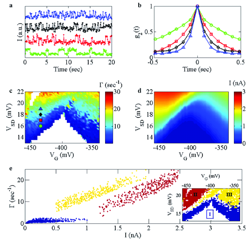
We map the dependence of the decay rate, , across the plane: for each value RTS was measured [Fig. 2(a)], the corresponding was calculated [Fig. 2(b)], and was extracted [Fig. 2(c)]. We find that is slower near the Coulomb blockade region, and becomes faster away from it. This behavior of nicely mirrors the current, , in the plane [Fig. 2(d)], indicating that the charging and discharging process of the trap is governed by the attempt rate of the flowing electrons. Figure 2(e) shows as a function of for points in the plane. Indeed, increases linearly with the current throughout, except for the Coulomb blockage region which will be discusses later.
We find a clear clustering of the measured decay rates into three groups [Fig. 2(e)]. The physical origin of this clustering can be understood by calculating the average charging state of the two dots at each value \bibnotemark[2]. We identify three main regions: the blockade [marked as I in Fig. 2(e)], in which the charging state is , the upper left region (II), in which an additional state, , contributes to the conduction, and the upper right region (III), with state. Here, is the number of excess electrons on the i’th dot. The clustering of follows these charging states: the two fast switching clusters (II and III) have the same average charge difference, , and differ in the average total charge, , while the slow region near the blockade (region I) is characterized by . We conclude that the trap dynamics is determined by the charging state of the two dots such that the electrostatic field between the dots, , acts as an effective drain-source field and the electrostatic potential, , acts as an effective gate.
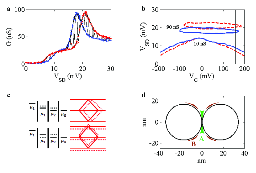
By examining the conductance, , we prove that the trap is indeed located between the dots near their surface. Figure 3(a) shows multiple scans of device A for a fixed value. This device exhibits a large RTS contrast [Fig. 1(d)], and, hence, it is easier to follow its conductance properties. It is seen that each conducting state (”on” or ”off”) is characterized by a distinct conductance spectrum, and the system jumps randomly from one to another. Hence, by measuring the conductance spectra for various values we can map the location of the conductance peaks of the two states in the plane [Fig. 3(b)]. We find that device A exhibits a rather surprising behavior, where the conductance peaks are shifted vertically with respect to each other.
Clearly, a trapped electron in the vicinity of the dimer shifts the two electrochemical potentials, and should induce a horizontal shift of the conductance spectrum in the plane [Fig. 3(c), top panel]. A significant vertical shift can only be obtained if an electron moves from one of the dots into a trap that is located between the dots. This process lowers the electrochemical potential of the first dot by , and raises the other by [Fig. 3(c), lower panel]. Here and are the individual and mutual charging energies of the dots, respectively.
We conduct a full numerical calculation of the induced gating of the two dots as a function of the trap location \bibnotemark[2]. This allows us to locate the traps in devices A and B as shown in Fig. 3(d). We find that the high contrast and vertical shift in device A are, indeed, due to a trap that is located in a rather small area, confined to the inter-dot region. The situation is somehow different for device B. Here we find a combination of horizontal and vertical shifts, with a smaller magnitude. This is consistent with a trap that is located slightly away from the central region between the dots, as depicted in Fig. 3(d). Indeed, we find a range of relative shifts in the seven measured devices, indicating that the trap may appear in different locations near the inter-dot region, restricted to a layer close to the surface of the dots \bibnoteA surface charge that is far away from the central region will not cause any significant effect, since it is equivalent to charging the dot by a full electron charge..
These location measurements suggest that the trap is related to the surrounding environment around the nanoparticles, i.e. the linking molecule or the capping layer. Indeed, the use of metallic nanoparticles allows us to rule out any trap within the nanoparticles volume. The linking molecule can be easily eliminated as the source for the trap - we studied the conductance of spontaneously formed dimers which did not contain the linking BPD molecule \bibnotemark[2], and observed a similar RTS behavior. The RTS signal was also found to be present in dimers which have a different capping layer (Na3citrate) 20, suggesting that the phenomenon is rather general and independent of the particular chemical composition of the layer. One may consider two types of traps that may give rise to the observed behavior: a region within the capping layer in which an electron may be localized, or a reconfiguration of a polar molecule, which is effectively equivalent to a movement of a charge near the nanoparticles 23. Further studies are needed to clarify the exact nature of the trap.
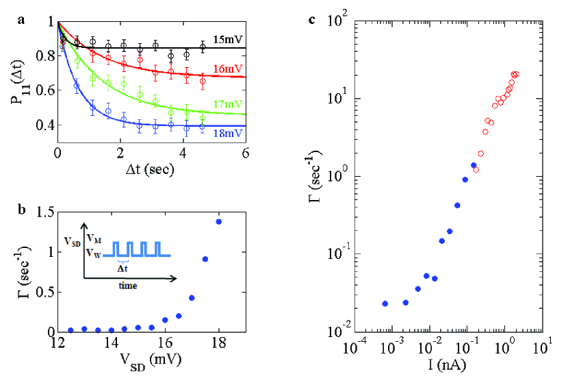
This system, a dimer with a charged trap, offers unique opportunities to control a single electron on macroscopic time scales and easily measure its state and dynamics. This control is demonstrated in Fig. 4, which shows that an electron can be trapped for extremely long times in the Coulomb blockade region. To extract in this region, where the current is very small and RTS cannot be detected, we performed the following sequence: We measured the conductance at a value, , outside the blockade and determine whether it is in the ”on” or ”off” state. We then switched the voltage into a lower value in the blockade, , and waited for a time duration at that voltage. Finally, we switched the voltage back to and measured again the conductance value [see inset of Fig. 4(b)]. This allowed us to determine the conditional probability to find the trap in the ”on” state at time if it was in the same state at time . Figure 4(a) shows this conditional probability for various values of . It is seen that as we lower and enter the blockade region the rate at which decays with becomes slower until it is nearly flat. Extracting the decay rate, , from these measurements, we find that it falls fast as we enter the Coulomb blockade regime and the occupation time of the trap exceeds a minute [Fig. 4(b)].
Combining the decay rates measured in the blockade region with the previous ones, outside the blockade [presented in Fig. 2(c)], we find a nice matching of the two sets of measurements [Fig. 4(c)]. It is seen that depends linearly on over several orders of magnitude: the slope of versus , plotted on a log-log scale, is approximately . We repeated this measurement with and found no decay of the probability up to minutes, implying that is much longer at this voltage \bibnotemark[2]. Since no current is flowing this isolated electron has limited interaction with the environment.
A clear demonstration of a single electron operation that can be realized in this system is the ability to ’write’ the trap state to the ”on” or ”off” position, and keep it for a desired duration \bibnotemark[2]. This is done by varying the applied voltages between two values. The ’readout’ is simply done by measuring the current through the device.
The characteristics of RTS in our system have many similarities with the optical blinking observed in semiconductor quantum dots 18, 19 and wires 24, in particular the abrupt switching between two distinct states, the relatively long time scales (order of seconds), and the current (intensity) dependence 25, 26. Furthermore, it is commonly accepted that optical blinking in these systems is due to a trapped charge at the surface 27, and there is a strong experimental evidence for a gating effect caused by this trapped charge 28, 29. These similarities suggest that the RTS observed in our work is the electrical manifestation of optical blinking, and can be used as a powerful tool to study this important effect.
We note, however, that there is a significant difference in the temporal statistics. While in our system the distribution of the ”on” and ”off” durations is exponential, the behavior in semiconductor dots is characterized by a power-law distribution 19. In fact, the first quantum dot blinking model, which attributed the phenomenon to a trapping of carrier on the surface, predicted an exponential distribution of the switching times 27. The origin of the power-law behavior remained not fully understood despite intense research in the last two decades 30. A series of modifications to the surface trap model have been proposed, in particular - the existence of multiple electron traps, varying with distance and/or trap depth, near the quantum dot surface 31. If this is indeed the origin of the power-law behavior, one can understand why it is not relevant in our system, where the effective traps are limited to a narrow area in the inter-dot region. We suggest that measurements of the electrical conductance of semiconductor quantum dots may be instrumental in deciphering the lingering question of optical blinking.
Nanoparticles synthesis and device fabrication methods, double-dot simulation, theoretical analysis of a trap dynamics, further measurements in the Coulomb blockade and demonstration of control, numerical calculations of the trap gating.
The authors declare no competing financial interest.
We would like to thank D. Mahalu and O. Raslin for their help in the electron beam lithography, and E. Cohen-Hoshen and J. Sperling for fruitful discussions on fabrication techniques.
[2]See Supporting Information
References
- van der Wiel et al. 2002 van der Wiel, W.; De Franceschi, S.; Elzerman, J. M.; Fujisawa, T.; Tarucha, S.; Kouwenhoven, L. P. Rev. Mod. Phys. 2002, 75, 1–22
- Loss and DiVincenzo 1998 Loss, D.; DiVincenzo, D. P. Phys. Rev. A 1998, 57, 120–126
- Kastner 1992 Kastner, M. Rev. Mod. Phys. 1992, 64, 849–858
- Petta et al. 2005 Petta, J. R.; Johnson, A. C.; Taylor, J. M.; Laird, E. A.; Yacoby, A.; Lukin, M. D.; Marcus, C. M.; Hanson, M. P.; Gossard, A. C. Science (New York, N.Y.) 2005, 309, 2180–4
- Maune et al. 2012 Maune, B. M.; Borselli, M. G.; Huang, B.; Ladd, T. D.; Deelman, P. W.; Holabird, K. S.; Kiselev, A. A.; Alvarado-Rodriguez, I.; Ross, R. S.; Schmitz, A. E.; Sokolich, M.; Watson, C. A.; Gyure, M. F.; Hunter, A. T. Nature 2012, 481, 344–7
- Banin et al. 1999 Banin, U.; Cao, Y.; Katz, D.; Millo, O. Nature 1999, 400, 542–544
- Feldheim and Foss 2002 Feldheim, D. L.; Foss, C. A. In Metal Nanoparticles: Synthesis, Characterization, and Applications, illustrate ed.; Feldheim, D. L., Foss, C. A., Eds.; Marcel Dekker, 2002; p 338
- Bolotin et al. 2004 Bolotin, K. I.; Kuemmeth, F.; Pasupathy, A. N.; Ralph, D. C. Appl. Phys. Lett. 2004, 84, 3154–3156
- Hu et al. 2007 Hu, Y.; Churchill, H. O. H.; Reilly, D. J.; Xiang, J.; Lieber, C. M.; Marcus, C. M. Nat. Nanotechnol. 2007, 2, 622–5
- Todd et al. 2009 Todd, K.; Chou, H.-T.; Amasha, S.; Goldhaber-Gordon, D. Nano Lett. 2009, 9, 416–21
- Guttman et al. 2011 Guttman, A.; Mahalu, D.; Sperling, J.; Cohen-Hoshen, E.; Bar-Joseph, I. Appl. Phys. Lett. 2011, 99, 063113
- Kane 1998 Kane, B. E. Nature 1998, 393, 133–137
- Tyryshkin et al. 2003 Tyryshkin, A. M.; Lyon, S. A.; Astashkin, A. V.; Raitsimring, A. M. Phys. Rev. B 2003, 68, 193207
- Jelezko et al. 2004 Jelezko, F.; Gaebel, T.; Popa, I.; Gruber, A.; Wrachtrup, J. Phys. Rev. Lett. 2004, 92, 076401
- Steinberg et al. 2010 Steinberg, H.; Wolf, O.; Faust, A.; Salant, A.; Lilach, Y.; Millo, O.; Banin, U. Nano Lett. 2010, 10, 2416–20
- Lachance-Quirion et al. 2014 Lachance-Quirion, D.; Tremblay, S.; Lamarre, S. A.; Méthot, V.; Gingras, D.; Camirand Lemyre, J.; Pioro-Ladrière, M.; Allen, C. N. Nano Lett. 2014, 14, 882–887
- Neel et al. 2011 Neel, N.; Kroger, J.; Berndt, R. Nano Lett. 2011, 11, 3593–6
- Nirmal et al. 1996 Nirmal, M.; Dabbousi, B. O.; Bawendi, M. G.; Macklin, J. J.; Trautman, J. K.; Harris, T. D.; Brus, L. E. Nature 1996, 383, 802–804
- Shimizu et al. 2001 Shimizu, K. T.; Neuhauser, R. G.; Leatherdale, C. A.; Empedocles, S. A.; Woo, W. K.; Bawendi, M. G. Phys. Rev. B 2001, 63, 205316
- Dadosh et al. 2005 Dadosh, T.; Gordin, Y.; Krahne, R.; Khivrich, I.; Mahalu, D.; Frydman, V.; Sperling, J.; Yacoby, A.; Bar-Joseph, I. Nature 2005, 436, 677–80
- 21 See Supporting Information
- 22 A surface charge that is far away from the central region will not cause any significant effect, since it is equivalent to charging the dot by a full electron charge.
- Schirm et al. 2013 Schirm, C.; Matt, M.; Pauly, F.; Cuevas, J. C.; Nielaba, P.; Scheer, E. Nat. Nanotechnol. 2013, 8, 645–8
- Glennon et al. 2007 Glennon, J. J.; Tang, R.; Buhro, W. E.; Loomis, R. a. Nano Lett. 2007, 7, 3290–5
- Banin et al. 1999 Banin, U.; Bruchez, M.; Alivisatos, a. P.; Ha, T.; Weiss, S.; Chemla, D. S. J. Chem. Phys. 1999, 110, 1195–1201
- Pistol et al. 1999 Pistol, M.-E.; Castrillo, P.; Hessman, D.; Prieto, J. A.; Samuelson, L. Phys. Rev. B 1999, 59, 10725–10729
- Efros and Rosen 1997 Efros, A. L.; Rosen, M. Phys. Rev. Lett. 1997, 78, 1110–1113
- Shimizu et al. 2002 Shimizu, K. T.; Woo, W. K.; Fisher, B. R.; Eisler, H. J.; Bawendi, M. G. Phys. Rev. Lett. 2002, 89, 117401
- Park et al. 2007 Park, S.-J.; Link, S.; Miller, W. L.; Gesquiere, A.; Barbara, P. F. Chem. Phys. 2007, 341, 169–174
- Frantsuzov et al. 2008 Frantsuzov, P.; Kuno, M.; Jankó, B.; Marcus, R. A. Nat. Phys. 2008, 4, 519–522
- Verberk et al. 2002 Verberk, R.; van Oijen, A. M.; Orrit, M. Phys. Rev. B 2002, 66, 233202