Thermoelectric properties of chalcopyrite type CuGaTe2 and chalcostibite CuSbS2
Abstract
Electronic and transport properties of CuGaTe2, a hole-doped ternary copper based chalcopyrite type semiconductor, are studied using calculations within the Density Functional Theory and solving the Boltzmann transport equation within the constant relaxation time approximation. The electronic bandstructures are calculated by means of the full-potential linear augmented plane wave method, using the Tran-Blaha modified Becke-Johnson potential. The calculated band gap of 1.23 eV is in agreement with the experimental value of 1.2 eV. The carrier concentration- and temperature dependent thermoelectric properties of CuGaTe2 are derived, and a figure of merit of is obtained at 950 K for a hole concentration of cm-3, in agreement with a recent experimental finding of , confirming that CuGaTe2 is a promising material for high temperature thermoelectric applications. The good thermoelectric performance of p-type CuGaTe2 is associated with anisotropic transport from a combination of heavy and light bands. Also for CuSbS2 (chalcostibite) a better performance is obtained for p-type than for n-type doping. The variation of the thermopower as a function of temperature and concentration suggests that CuSbS2 will be a good thermoelectric material at low temperatures, similarly to the isostructural CuBiS2 compound.
I Introduction
Thermoelectric (TE) materials with potential applications within power generation and refrigeration have represented a thrust area of research for the past few decades. TE materials can convert waste heat into electric power and hence play a vital role in meeting the present condition of energy crisis and environment pollution.Majumdar ; Bell ; Snyder ; Dress The performance of a TE material is reflected in the dimensionless figure of merit, , given by , where , , and are the thermopower, the electrical conductivity, the thermal conductivity, and the absolute temperature, respectively. includes both the electronic, , and the lattice contributions, , i.e. . From this expression, it is evident that finding materials with high is a challenge, as it appears that such a material should satisfy the conflicting requirements of high thermopower, which is often found for doped insulators, and behave as a good electrical conductor like a metal with a low thermal conductivity. Good electrical conductivity and poor thermal conductivity implies a weak electron scattering and strong phonon scattering. Remarkable progress has been made in recent years exploring different classes of materials for better TE performance.Snyder ; Dress ; Georg ; singh ; Abdeljalil ; Jiong ; andrew ; Wang ; Jovovic ; David ; YuLi ; khu ; Lijun ; Parker ; Khuong ; Mun Few materials with are known.Snyder Apart from the material properties necessary for a good figure of merit, there are also other materials properties to be considered. The materials should possess a high melting point as far as waste heat recovery is concerned, and they should be structurally stable in the operating temperature range. In addition, the constituents of the materials should be abundant and in-expensive. The real success in the field of thermoelectrics lies in identifying a material with all the desired properties. There are few commonly used good TE materials such as PbTe and Bi2Te3.Satterwaithe ; Goldsmid ; DJS Bi2Te3 can be hole doped and electron doped and has at room temperature, but still it has a shortfall as Te is a rare element and has many restrictions for large-scale applications.cubis2 ; Amatya Recently, alternative Pb-free materials such as AgGaTe2 and CuBiS2, have been considered.cubis2 ; Wentao ; aggate2 The present work on the chalcopyrite semiconductor CuGaTe2 is motivated by the recent experimental work ADV. MATER reporting a of 1.4 at temperatures above 800 K for this compound. Although many of the PbTe based materials may also have , their range of operating temperature is much lower than that of CuGaTe2.K. F. Hsu ; Y. Pei ; Biswas ; Poudeu ; Androulakis ; Pei Ab-inito calculations for the similar chalcopyrite compound AgGaTe2 were performed by Parker and Singhcubis2 and Wu et al.,Wentao who showed that hole doping of AgGaTe2 improves its TE performance. The present work is a theoretical analysis of CuGaTe2, which supports the classification of this compound as an excellent thermoelectric material. In addition, also CuSbS2 is examined. This compound is isostructural with CuBiS2, which has been predicted to be an excellent TE material.cubis2
The paper is organized as follows: Section II describes the method used for the calculations, and section III presents the results and a discussion. Conclusions are given in section IV.
II Methodology
The electronic band structures were calculated by means of the full-potential linear augmented plane wave (FP-LAPW) method based on first-principles density functional theory as implemented in the WIEN2k code.Blaha Since calculations using standard local-density (LDA) or Generalized Gradient Approximation (GGA) schemes for the exchange-correlation potential underestimate the band gaps of semiconductors, we have used the modified GGA known as the Tran-Blaha modified Becke-JohnsonBecke potential (TB-mBJ).Tran1 For k-space integrations a 20x20x20 k-mesh was used for CuGaTe2 and 19x31x8 k-mesh for CuSbS2 in the Monkhorst-Pack scheme, resulting in 641 and 800 k-points in the irreducible parts of the Brillouin zones for the two compounds, respectively. The self-consistent calculations included spin-orbit coupling. The crystal structure of CuGaTe2 is tetragonal with space group (no. 122) and lattice parameters a=6.028 Å and c=11.949 Å.Kuhn For CuSbS2, the crystal structure is in the orthorhombic space group (no. 62) with lattice parameters a=6.018 Å, b=3.7958 Å and c=14.495 Å.Atsushi All the calculations were performed with the experimental lattice parameters with an energy convergence criterion of Ry per formula unit. The carrier concentration (p for holes and n for electrons) and temperature () dependent thermoelectric properties like thermopower (), electrical conductivity (), power factor (), and figure of merit () were calculated using the BOLTZTRAPMadsen code, within the Rigid Band Approximation (RBA)Scheidemantel ; Jodin and the constant scattering time () approximation (CSTA). In the RBA the band structure is assumed unaffected by doping, which only leads to a shift of the chemical potential. For semiconductors it is a good approximation for calculation of the transport properties, when the doping level is not too high.Jodin ; Chaput ; Bilc ; Ziman ; Nag ; Mazin In the CSTA, the scattering time of electrons is assumed independent of the electron energy, while it may depend on carrier concentration and temperature. A detailed discussion of the CSTA is given in Refs. singh, , aggate2, and Khuong, , and references therein. The only situation where the CSTA can fail is when bipolar conduction is significant, which happens in narrow-gap materials. According to Sofo and Mahan,sofo the best performance of a thermoelectric material is found when the energy gap is about 10 kBTo, where To is the operating temperature, as far as direct band gap materials are concerned. In the case of CuGaTe2, which is found to have a direct band gap of about 1.2 eV, this corresponds to To 1400 K. According to the present calculations reaches its maximum value near 950 K, and this justifies the approximation used in the calculations for CuGaTe2, as we are still far away from the region of bipolar conduction. In the case of CuSbS2, the band gap around 1 eV corresponds to To 1200 K, however the melting point iswachtel only 825 K. Therefore, the present calculations for CuSbS2 cover only temperatures up to 700 K, again a safe regime as far as the CSTA is concerned.
III Results and Discussion
III.1 Band structure and Density of States of CuGaTe2 and CuSbS2
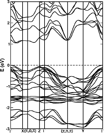
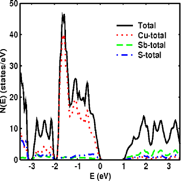
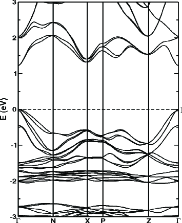
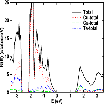
The calculated band structure of CuGaTe2 along the high symmetry directions of the tetragonal Brillouin zone is shown in FIG. 1(a). The valence band maximum (VBM) (zero energy in the band structure plot) and the conduction band minimum (CBM) are both located at the centre of the Brillouin zone i.e. at the -point, making the compound a direct-band-gap semiconductor. The band gap values obtained within the GGA and the TB-mBJ are given in Table I. From the large band gaps it is expected that there should not be any bipolar conduction. The band structure in the vicinity of the VBM exhibits a mixture of heavy and light bands, which is often favourable for thermoelectric performance, one can also see here such a situation in the vicinity of the VBM. The heavy band found just below the VBM arises from the Cu-d and Te-p states, and below this lies the light band of Te-p and Ga-d character. The Density of States (DOS) of CuGaTe2 is shown in FIG. 1(b), where it is apparent that the major contribution to the bands at the VBM comes from the Cu-d states, leading to a strong increase in the DOS as energy is moving away from the VBM. Similarly, the DOS also rises steeply above the CBM, albeit not as distinctly as around the VBM, cf. FIG. 1(a) and 1(b). The heavy bands usually contribute to a high thermopower while the lighter bands offer an advantage of high mobility, a favorable combination often leading to an excellent TE performance of the material. Although one might also expect that n-doping could give good thermoelectric performance for CuGaTe2, the presence of multiple heavy bands at the VBM would likely favour the p-type doping over n-type, as is indeed found in the succeeding subsection, where the transport properties and optimized doping level are discussed.
For CuSbS2 the calculated band structure along the high symmetry directions of the orthorhombic Brillouin zone is shown in FIG. 2(a). This compound is an indirect-band-gap semiconductor with a band gap of 1.05 eV, where experimental gap values are somewhat higher, 1.38 eVZhou and 1.52 eVRodriguez (see Table I). The gap is large enough to prevent bipolar conduction for operating temperatures below the melting point. The bands near the -point are dispersive in all three symmetry directions, albeit least dispersive along -Z. The DOS of CuSbS2 is shown in FIG. 2(b), from which it is seen that the major contribution to the DOS near the VBM comes from the Cu-d states. Compared to the DOS of CuGaTe2, there is less symmetry between the CBM and VBM regimes, which would render p-type doping more favorable over n-type doping in CuSbS2 than in CuGaTe2. The presence of the heavy mass band at the VBM for both compounds indicates the possibility for excellent thermo-electric performance. This is discussed in the following section.
III.2 Thermoelectric properties of CuGaTe2 and CuSbS2
The carrier concentration and temperature dependent thermoelectric properties of CuGaTe2 are obtained by solving the Boltzmann transport equation as implemented in the BOLZTRAPMadsen code. The calculated properties are the thermopower, the electrical conductivity divided by the scattering time (i.e. /), the power factor, and the figure of merit as functions of carrier concentration and temperature. Since most of the experiments are done in poly-crystalline samples, we have calculated the averages of the thermopower and the electrical conductivity (respectively) over three orthogonal axes in order to estimate the figure of merit. Due to the lack of experimental data for CuSbS2 from which the relaxation time may be extracted (temperature dependent concentration and resistivity), we have for this compound only studied the concentration and temperature dependent thermopower, and concentration dependent / ratio.
III.2.1 Thermopower
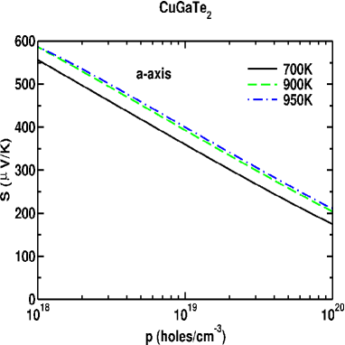
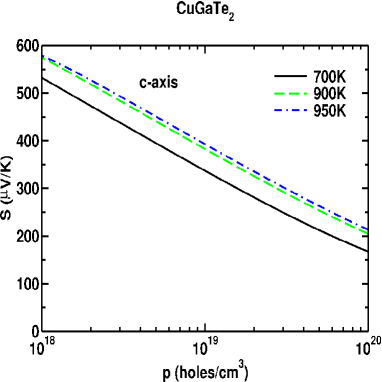
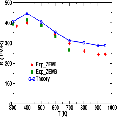
The calculated value of depends on carrier concentration and temperature, but it is independent of due to the CSTA. The calculated thermopower for CuGaTe2, , as a function of hole concentration at different temperatures along the a- and c-axes is shown in Figs. 3(a) and 3(b). The trend of the thermopower along the two axes is similar to what has been found for other thermoelectric materials with the tetragonal structure.Khuong ; aggate2 It is also seen that the thermopower increases with decreasing carrier concentration.The Pisarenko behavior, i.e. logarithmic variation of the thermopower with carrier concentration, is found in the range of – cm-3, which is an optimum working region for good thermoelectric materials. The variation of the thermopower of CuGaTe2 as a function of temperature was measured by Plirdpring et al.ADV. MATER These authors also determined the temperature dependent carrier density , so by combining this information with the calculated , the calculated temperature dependent thermopower may be obtained and compared directly to experiment. This is done in FIG. 4. The theory and experiment are in good agreement with a qualitatively similar shape and a maximum thermopower around 400 K (maximal thermopower of 450 V/K and 410 V/K in theory and experiment, respectively). At 900 K the thermopower has fallen to around 250 V/K. At 950 K, where the measured figure of merit has its maximum value (about ), an experimental thermopower of V/K is measured,ADV. MATER as compared to the theoretical value of V/K.
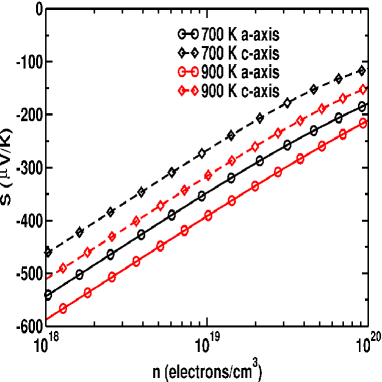
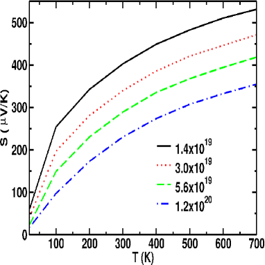
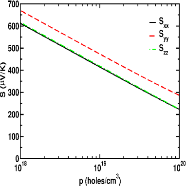
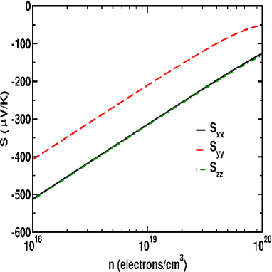
It is interesting to examine the thermopower also in the case of electron doping, which is illustrated in FIG. 5, showing the thermopower variation with electron concentration at different temperatures and along both the a and c axes. The magnitude of the thermopower is about the same for given carrier density for p- and n-type doping, about 400 V/K at cm-3 and 900 K, however the anisotropy is larger in the case of n-type doping. From FIG. 5 the difference in the thermopower along and is 65 V/K (larger along ), which is about twice as large as in p-type doped CuGaTe2 (FIG. 3). This might be unfavorable for the potential use of n-type doped CuGaTe2 as a thermoelectric material.aggate2 The variation of the thermopower with temperature for CuSbS2 at selected hole concentrations is displayed in FIG. 6(a). The thermopower increases with decreasing carrier concentration as in all good TE materials. The melting point of CuSbS2 is relatively low, K,wachtel and hence this compound is less suited for high temperature applications, however it may find application as a cooling component, similar to the isostructural CuBiS2 compound.cubis2 To investigate the anisotropy of thermoelectric properties we have calculated the directional dependent thermopower as function of the hole and electron concentration as shown in FIG. 6(b, c). From the figure, it appears that the thermopower is very similar in the the and directions, while it is higher in the direction by about 70 V/K for hole doping and numerically lower by 100 V/K for electron doping. Thus, the thermopower for hole doping is somewhat larger than for electron doping, assuming similar carrier densities. The magnitude of the thermopower for hole doping is similar to what is found for the isostructural CuBiS2,cubis2 while the anisotropy is somewhat larger.
III.2.2 Electrical conductivity
The electrical conductivity may be estimated for CuGaTe2 by a combination of theory and experiment. This requires that, the scattering time is estimated, which is possible from the experiments of Ref. ADV. MATER, , if the scattering time is assumed to be a function of temperature alone, i.e. . The calculated ratio is a function of and carrier concentration , i.e. . In the experiments the carrier concentration itself is a function of temperature and displayed in Fig. 3 of Ref. ADV. MATER, . The experimental data are available up to 800 K, and we have extrapolated in order to get the concentration up to 950 K. The scattering time then follows from the relation
Here, and are the measured conductivity and carrier concentration, respectively, while is the calculated ratio. Subsequently, we may obtain as a function of two variables by multiplying the calculated ratio by :
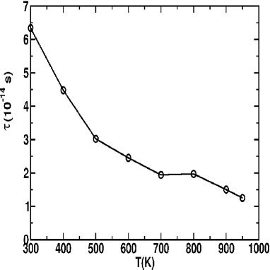
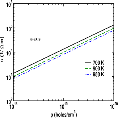
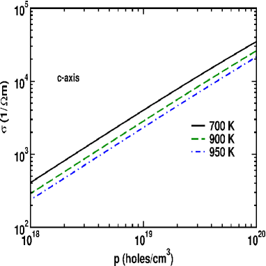
The scattering time obtained in this way is displayed in figure 7. A similar procedure was adopted by Ref. Khuong, , however using only one value and assuming phonon-dominated scattering. Fig. 8 shows the obtained electrical conductivity () along the a- and c- directions as functions of hole concentration. The electrical conductivity increases in both cases essentially linearly with the carrier concentration, as also found in Drude’s model. The conductivity is significantly higher along the -axis than along the -axis, approximately by a factor of 5. The electrical conductivity is a decreasing function of temperature for given carrier density, mainly reflecting the temperature dependence of the scattering time.
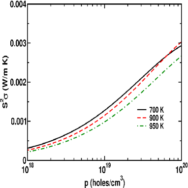
Having the thermopower and the electrical conductivity, the power factor (S2) is calculated and displayed in FIG. 9 as function of carrier concentration for three representative temperatures. At 950 K, the calculated power factor at the experimentally realized carrier concentration of cm-3 (present authors’ extrapolation of data from Ref. ADV. MATER, ) is mW/m K2, which is in fair agreement with the corresponding measured valueADV. MATER of 1.35 mW/m K2.
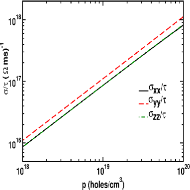
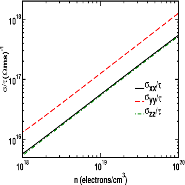
In the case of CuSbS2 the calculated variation of the / ratio with hole and electron concentration at 300 K is shown in FIG. 10(a,b). The / varies almost isotropically with a little difference seen along the b-axis, which is similar to the trend observed in the thermopower, FIG. 6(b,c). The / ratio is higher for hole doping than for electron doping, so for similar carrier density and similar scattering times, this implies better TE performance for p-type CuSbS2. As there are no experimental data available for this compound, we were not able to proceed to find the electrical conductivity as in the case of CuGaTe2.
III.2.3 Thermal Conductivity and
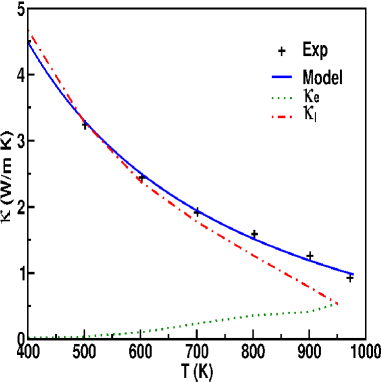
To calculate the figure of merit the thermal conductivity must be known. This was taken from the experiment.ADV. MATER is the sum of the electronic and the lattice thermal conductivities, , and these authors showed that if the electronic thermal conductivity is obtained from the Wiedemann-Franz (WF) relation , using the Lorentz number ( W / K2), the lattice contribution is well described with an inverse law, i.e. , in the range 400-800 K, as applicable to Umklapp scattering. The WF relation is valid for metals, whereas more accurate modeling may be needed in some cases for semiconductors, see Ref. EES2012, and references therein. At temperatures above 800 K the lattice thermal conductivity seems to fall more steeply than dictated by the Umklapp law.ADV. MATER Following Ong et al.Khuong (for the case of n-type ZnO) we have found that the experimental lattice conductivity is well approximated in the full range 400-950 K by a fit of the form , with W/m and W/m K. This is illustrated in FIG. 11, which also shows the above WF and Umklapp contributions.
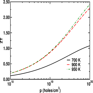
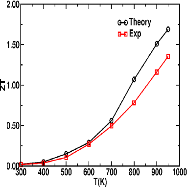
From the experimental information regarding the thermal conductivity, we may calculate the figure of merit as function of carrier concentration and temperature as illustrated in FIG. 12. FIG. 12(a) shows for three temperatures the carrier dependence of the figure of merit, which is rising above for carrier densities above cm-3. Such high carrier densities are not encountered in experiment, so for a better comparison with experiment the factor evaluated for the experimental carrier density (Ref. ADV. MATER, ) is displayed in FIG. 12(b). Here the theoretical figure of merit reaches a value of at K, in perfect agreement with the experimental value of at this temperature.ADV. MATER The experimental carrier density at K is only cm-3, as extrapolated from Fig. 3 of Ref. ADV. MATER, , i. e., significantly lower than the optimum density indicated from FIG. 12(a). This high figure of merit indeed renders CuGaTe2 a promising material for high temperature thermoelectric applications. Furthermore, under the same conditions, the Seebeck coefficient is calculated to be 287 V/K in good agreement with the measured value of 244 V/K.ADV. MATER
IV Conclusion
Electronic transport properties of CuGaTe2 and CuSbS2 were calculated using density functional theory. Both compounds were found to be very good thermoelectric materials with p-type doping. A somewhat anisotropic character of the thermopower and electrical conductivity as functions of hole concentration was found in both compounds. In the case of hole doped CuGaTe2 with a concentration of cm-3, we obtained a figure of merit and a thermopower of 287 V/K at 950 K, in excellent agreement with the reported experimental value. In the case of CuSbS2 the Seebeck coefficient was found to be large, e.g. at room temperature the calculated thermopower exceeds 400 V/K for a hole concentration of cm-3. The melting point of this compound is low, and high-temperature thermoelectric applications will be impractical, but this material might be suitable for low temperature applications.
V Acknowledgement
V.K.G. and V.K. would like to acknowledge IIT-Hyderabad for providing computational facility. V.K.G. would like to thanks MHRD for the fellowship. V.K. thanks NSFC awarded Research Fellowship for International Young Scientists under Grant No. 11250110051. G.V. thanks Center for Modelling Simulation and Design-University of Hyderabad (CMSD-UoH) for providing access to its computational facilities.
*Author for Correspondence, E-mail: kanchana@iith.ac.in
References
- (1) A. Majumdar, Science 303, 777-778 (2004).
- (2) L. E. Bell, Science 321, 1457-1461 (2008).
- (3) G. J. Snyder, and E. S. Toberer, Nat. Mater. 7, 105-114 (2008).
- (4) M. Zebarjadi, K. Esfarjani, M. S. Dresselhaus, Z. F. Ren, and G. Chen, Energy Environ. Sci. 5, 5147-5162 (2012).
- (5) G. K. H. Madsen, K. Schwarz, P. Blaha, and D. J. Singh, Phys. Rev. B 68, 125212 (2003).
- (6) D. J. Singh, Funct. Mat. Lett. 3, 223-226 (2010).
- (7) A. Assoud, Y. Cui, S. Thomas, B. Sutherland, and H. Kleinke, J. Solid State Chem. 181, 2024 (2008).
- (8) J. Yang, H. Li, T. Wu, W. Zhang, L. Chen, and J. Yang, Adv. Func. Mater. 18, 2880-2888 (2008).
- (9) A. F. May, D. J. Singh, and G. J. Snyder, Phys. Rev. B 79, 153101 (2009).
- (10) L. L. Wang, L. Miao, Z. Y. Wang, W. Wei, R. Xiong, H. J. Liu, J. Shi, and X. F. Tang, J. Appl. Phys. 105, 013709 (2009).
- (11) V. Jovovic, and J. P. Heremans, J. Electron. Mater. 38, 1504-1509 (2009).
- (12) D. Parker, and D. J. Singh, J. Appl. Phys. 108, 083712 (2010).
- (13) Y. L. Yan, and Y. X. Wang, Appl. Phys. Lett. 97, 252106 (2010).
- (14) K. P. Ong, D. J. Singh, and P. Wu, Phys. Rev. Lett. 104, 176601 (2010).
- (15) L. Zhang, M.-H. Du, and D. J. Singh, Phys. Rev. B 81, 075117 (2010).
- (16) D. Parker, and D. J. Singh, Phys. Rev. B 82, 035204 (2010).
- (17) K. P. Ong, D. J. Singh, and P. Wu, Phys. Rev. B 83, 115110 (2011).
- (18) E. D. Mun, S. L. Bud’ko, and P. C. Canfield, J. Phys.: Condens. Matter 23, 476001 (2011).
- (19) C. B. Satterwaithe, and R. W. Ure Jr., Phys. Rev. 108, 1164 (1957).
- (20) H. J. Goldsmid, A. R. Sheard, and D. A. Wright, Br. J. Appl. Phys. 9, 365 (1958).
- (21) D. J. Singh, Phys. Rev. B 81, 195217 (2012).
- (22) D. Parker, and D. J. Singh, Phys. Rev. B 83, 233206 (2011).
- (23) R. Amatya and R.J. Ram, J. Electron. Mater. 41, 1011 (2012).
- (24) W. Wu, K. Wu, Z. Ma, and R. Sa, Chem. Phys. Lett. 537, 62 (2012).
- (25) D. Parker, and D. J. Singh, Phys. Rev. B 85, 125209 (2012).
- (26) T. Plirdpring, K. Kurosaki, A. Kosuga, T. Day, S. Firdosy, V. Ravi, G. J. Snyder, A. Harnwunggmoung, T. Sugahara, Y. Ohishi, H. Muta, and S. Yamanaka, Adv. Mater. 24, 3622–3626 (2012).
- (27) K. F. Hsu, S. Loo, F. Guo, W. Chen, J. S. Dyck, C. Uher, T. Hogan, E. K. Polychroniadis, and M. G. Kanatzidis, Science 303, 818-821 (2004).
- (28) Y. Pei, J. Lensch-Falk, E. S. Toberer, D. L. Medlin, and G. J. Snyder, Adv. Funct. Mater. 21, 241-249 (2011).
- (29) K. Biswas, J. He, Q. Zhang, G. Wang, C. Uher, V. P. Dravid, and M. G. Kanatzidis, Nat. Chem. 3, 160-166 (2011).
- (30) P. F. P. Poudeu, J. D’Angelo, A. D. Downey, J. L. Short, T. P. Hogan, and M. G. Kanatzidis, Angew. Chem. Int. Ed. 45, 3835 (2006).
- (31) J. Androulakis, C.-H. Lin, H.-J. Kong, C. Uher, C.-I. Wu, T. Hogan, B. A. Cook, T. Caillat, K. M. Paraskevopoulos, and M. G. Kanatzidis, J. Am. Chem. Soc. 129, 9780 (2007).
- (32) Y. Pei, X. Shi, A. LaLonde, H. Wang, L. Chen, and G. J. Snyder, Nature 473, 66 (2011).
- (33) P. Blaha, K. Schwarz, G. K. H. Madsen, D. Kvasnicka, and J. Luitz, WIEN2K, An augmented plane wave + local orbitals program for calculating crystal properties. (Karlheinz Schwarz, Techn. Universität Wien, Austria), 2001.
- (34) A. D. Becke, and E. R. Johnson, J. Chem. Phys. 124, 221101 (2006).
- (35) F. Tran, and P. Blaha, Phys. Rev. Lett. 102, 226401 (2009).
- (36) B. Kuhn, W. Kaefer, K. Fess, K. Friemelt, Ch. Turner, M. Wendl, and E. Bucher, Phys. Stat. Sol. (a) 162, 661 (1997).
- (37) A. Kyono, and M. Kimata, Am. Miner. 90, 162 (2005).
- (38) G. K. H. Madsen, and D. J. Singh, Comput. Phys. Commun. 175, 67-71 (2006).
- (39) T. J. Scheidemantel, C. Ambrosch-Draxl, T. Thonhauser, J. V. Badding, and J. O. Sofo, Phys. Rev. B 68, 125210 (2003).
- (40) L. Jodin, J. Tobola, P. Pecheur, H. Scherrer, and S. Kaprzyk, Phys. Rev. B 70, 184207 (2004).
- (41) L. Chaput, P. Pecheur, J. Tobola, and H. Scherrer, Phys. Rev. B 72, 085126 (2005).
- (42) D. I. Bilc, S. D. Mahanti, and M. G. Kanatzidis, Phys. Rev. B 74, 125202 (2006).
- (43) J. M. Ziman, Electrons and Phonons: Theory of Transport Phenomena in Solids (Oxford University Press, London, UK, 1960).
- (44) B. R. Nag, Electron Transport in Compound Semiconductors (Springer-Verlag, Berlin, 1980).
- (45) D. J. Singh, and I. I. Mazin, Phys. Rev. B 56, R1650 (1997).
- (46) J. O. Sofo, and G. D. Mahan, Phys. Rev. B 49, 4565 (1994).
- (47) A. Wachtel, and A. Noreika, J. Electron. Mater. 9, 281 (1980).
- (48) J. Zhou, G.-Q. Bian, Q.-Y. Zhu, Y. Zhang, C.-Y. Li, and J. Dai, J. Solid State Chem. 182, 259 (2009).
- (49) Y. Rodrguez-Lazcano, M. Nair and P. Nair, J. Cryst. Growth 223, 399 (2001).
- (50) Y. Pei, A. D. LaLonde, H. Wang, and G. J. Snyder, Energy Environ. Sci. 5, 7963 (2012).
| CuGaTe2 | CuSbS2 | ||
|---|---|---|---|
| GGA | 0.57 | 0.77 | |
| TB-mBJ | 1.23 | 1.05 | |
| Expt. | 1.2a | 1.38b, 1.52c |
a: Ref. ADV. MATER, ; b: Ref. Zhou, ; c: Ref. Rodriguez, .
.
