Electron-hole pairing in graphene-GaAs heterostructures
Abstract
Vertical heterostructures combining different layered materials offer novel opportunities for applications novoselov_ps_2012 ; bonaccorso_matertoday_2012 ; britnell_science_2012 and fundamental studies of collective behavior driven by inter-layer Coulomb coupling ponomarenko_naturephys_2011 ; kim_prb_2011 ; gorbachev_naturephys_2012 ; kim_ssc_2012 . Here we report heterostructures comprising a single-layer (or bilayer) graphene carrying a fluid of massless (massive) chiral carriers andre_naturemater_2007 , and a quantum well created in GaAs 31.5 nm below the surface, supporting a high-mobility two-dimensional electron gas. These are a new class of double-layer devices composed of spatially-separated electron and hole fluids. We find that the Coulomb drag resistivity significantly increases for temperatures below 5-10 K, following a logarithmic law. This anomalous behavior is a signature of the onset of strong inter-layer correlations, compatible with the formation of a condensate of permanent excitons. The ability to induce strongly-correlated electron-hole states paves the way for the realization of coherent circuits with minimal dissipation high_science_2008 ; kuznetsova_opticsletters_2010 ; sanvitto_naturecommun_2013 and nanodevices including analog-to-digital converters dolcini_prl_2010 and topologically protected quantum bits peotta_prb_2011 .
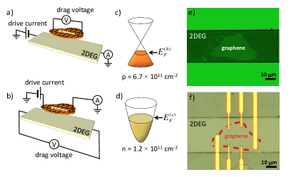
Our vertical heterostructures are prepared as follows. Single-layer (SLG) and bilayer graphene (BLG) flakes are produced by micromechanical exfoliation of graphite on Si/ kostya_pnas_2005 . The number of layers is identified by a combination of optical microscopy cnano and Raman spectroscopy RamanACF ; RamanACF2 . The latter is also used to monitor the sample quality by measuring the D to G ratio cancado and the doping level das . Selected flakes are then placed onto a GaAs-based substrate at the center of a pre-patterned Hall bar by using a polymer-based wet transfer process bonaccorso_matertoday_2012 (see Appendix A for further details). The GaAs-based substrates consist of modulation-doped GaAs/AlGaAs heterostructures hosting a two-dimensional electron gas (2DEG) in the GaAs quantum well placed below the surface. The heterostructures are grown by molecular beam epitaxy loren , and consist of a -doped GaAs cap layer, a AlGaAs barrier, a GaAs well and a thick AlGaAs barrier with a delta doping layer (see Appendix A for further details). Two different samples are fabricated: sample A having a -thick quantum well and sample B with a -thick quantum well. Hall bars ( wide and long) are fabricated by UV lithography. Ni/AuGe/Ni/Au layers are then evaporated and annealed at to form Ohmic contacts to the 2DEG, to be used for transport and Coulomb drag measurements (see Fig. 1). The Hall bar mesas are defined by conventional wet etching in acid solution. To ensure that the current in the 2DEG flows only in the region below the graphene flakes, channels with a width comparable to the transferred graphene flakes (typically ), are defined in the Hall bar by means of electron beam lithography and wet etching, Figs. 1e)-f). A SLG flake is transferred onto sample A and a BLG flake onto sample B. The integrity of the SLG and BLG flakes is monitored throughout the process by Raman spectroscopy. Fig. 6 in Appendix A compares the Raman spectra of as prepared SLG on Si/SiO2 and after transfer on the GaAs substrate. Analysis of G peak position, Pos(G), its full width at half maximum, FWHM(G), Pos(2D) and the area and intensity ratios of 2D and G peaks, allow us to monitor the amount and type of doping RamanACF2 ; das ; basko . This indicates a small doping for the as-prepared sample, decreasing to below for the transferred sample RamanACF2 ; das ; basko . The absence of a significant D peak both before and after transfer indicates that the samples have negligible amount of defects cancado ; RamanACF2 and that the transfer procedure does not add defects. Similarly, no increase in defects is seen for the BLG samples.
To ensure that the two-dimensional (2d) hole gas in SLG/BLG and the 2DEG in GaAs are electrically isolated, we monitor the inter-layer - characteristics in the - temperature range (see Appendix C), with and the inter-layer (“leakage”) current and inter-layer voltage, respectively, and the layers being the SLG (or BLG) and the GaAs quantum well. In SLG-based devices, a negligible inter-layer current is measured for up to for all temperatures, leading to inter-layer resistances . In the case of BLG, for , increases to at , with the inter-layer resistance increasing to several . In all cases, therefore, the inter-layer resistance is much larger than the largest intra-layer resistance for SLG, BLG and GaAs quantum well, which is .
To search for signatures of correlations between the 2DEG in the GaAs quantum well and the chiral hole fluid andre_naturemater_2007 in SLG or BLG, we measure the temperature dependence of the Coulomb drag resistance . In a Coulomb drag experiment gramila_prl_1991 ; sivan_prl_1992 ; rojo_jpcm_1999 a current source is connected to one of the two layers (the active or drive layer). The other layer (the passive layer) is connected to an external voltmeter, so that the layer can be assumed to be an open circuit (no current can flow in it). The drive current drags carriers in the passive layer, which accumulate at the ends of the layer, building up an electric field. The voltage drop related to this field is then measured. The quantity is defined as the ratio and is determined by the rate at which momentum is transferred between quasiparticles in the two layers rojo_jpcm_1999 .
Since originates from electron-electron interactions, it contains information on many-body effects stemming from correlations zheng_prb_1993 ; kamenev_prb_1995 . Experimentally, Coulomb drag has been indeed used as a sensitive probe of transitions to the superconducting state giordano_prb_1994 , metal-insulator transitions pillarisetty_prb_2005 , transition to the Wigner crystal phase in quantum wires yamamoto_science_2006 , and exciton condensation in quantum Hall bilayers nandi_nature_2012 . In the context of spatially-separated systems of electrons and holes, in the absence of a magnetic field, the theoretical studies in Ref. vignale_prl_1996, indicated that is comparable to the isolated layer resistivity in the exciton condensed phase of an electron-hole (e-h) double layer. For larger than, but close to, the mean-field critical temperature , the occurrence of e-h pairing fluctuations increases with respect to its value in the Fermi-liquid phase hu_prl_2000 ; snoke_science_2002 ; mink_prl_2012 ; mink_prb_2013 . An increase in with a suitable functional dependence on indicates the transition to an exciton condensate hu_prl_2000 ; snoke_science_2002 ; mink_prl_2012 ; mink_prb_2013 . This is similar to the enhancement of conductivity in superconductors due to Cooper-pair fluctuations (“paraconductivity”) above, but close to, the critical temperature Larkin_and_Varlamov .
Prior to Coulomb drag experiments, we perform magneto-transport measurements at , as for Figs. 2a)-b). In our setup, the 2DEG is induced in the quantum well by shining light from an infrared diode. In the SLG/2DEG device we find a 2DEG with density from low-field (below 1 Tesla) classical Hall effect and a mobility at 4K. At , the density decreases to and . Fig. 2a) shows the quantum Hall effect in the 2DEG. The quantum Hall plateaus at and (blue trace), correspond to the first two spin degenerate Landau levels prange . In correspondence of the plateaus, minima are found prange in the longitudinal resistance (red trace).
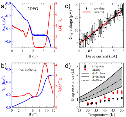
The 2d hole fluids in SLG and BLG have their highest mobility when the 2DEG is not induced. This is shown in Fig. 2b) for the SLG-based device (see also Appendix B). Figs. 2a)-b) indicate that the sign of the Hall resistance in SLG is opposite to the 2DEG, thereby demonstrating that SLG is -doped. At the hole density is and . At the corresponding values are and . Low-temperature magneto-transport in SLG, Fig. 2b), reveals quantum Hall plateaus at and , corresponding to massless Dirac fermions with spin and valley degeneracy andre_naturemater_2007 . On the contrary, when the 2DEG is optically induced, the hole density in SLG at is and , thereby weakening the manifestations of the quantum Hall effect (see Appendix B). The degradation of the SLG transport properties in the presence of the 2DEG could be linked to the creation of ionized Si donors within the -doped GaAs cap layer, acting as positively-charged scatterers dassarma_rmp_2011 .
We now focus on the Coulomb drag experiments. These are performed in the configuration sketched in Figs. 1a)-b) and in a 3He cryostat with a - temperature range. Ten - curves in a dc configuration are acquired for each and then averaged. We first address the SLG/2DEG case. Fig. 2c) reports a representative set of averaged drag voltage data taken in the 2DEG at . In this configuration, the SLG gating effect and consequent carrier depletion in the 2DEG are avoided by applying a positive current, from 0 to A in the SLG channel. Fig. 2c) shows that at this representative value of the drag voltage is linear with the drive current, thereby allowing the extraction of from the slope of a linear fit.
Fig. 2d) plots for , with the 2DEG used as the drive (black points) or passive (red points) layer. It also reports calculations of the dependence of in a hybrid Dirac/Schrödinger SLG/2DEG double layer within a Boltzmann-transport theory, which is justified in the Fermi-liquid regime carrega_njp_2012 ; principi_prb_2012 . This is done by generalizing the theory of Ref. principi_prb_2012, to include effects due to the finite width of the GaAs quantum well (see Appendix E). This shows that the experimental results in this temperature range are consistent with the canonical Fermi-liquid prediction gramila_prl_1991 ; sivan_prl_1992 ; rojo_jpcm_1999 ; zheng_prb_1993 ; kamenev_prb_1995 ; carrega_njp_2012 ; principi_prb_2012 , i.e. —see also Fig. 3a)—as constrained by the available phase-space of the initial and final states involved in the scattering process. The magnitude of the measured effect, however, is smaller than predicted by theory. Discrepancies of similar magnitude have been previously reported for Coulomb drag measurements between two SLG encapsulated in hexagonal Boron Nitride gorbachev_naturephys_2012 . Fig. 2d) demonstrates that the Onsager reciprocity relations onsager_physrev_1931_I ; onsager_physrev_1931_II , which in our case require that the resistance measured by interchanging drive and passive layers should be unchanged, are satisfied in the range. A slight violation of reciprocity, whose origin is at present not understood, seems to occur for .
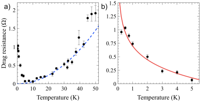
We now discuss the behavior of in the low- regime. We follow Ref. gorbachev_naturephys_2012, and use the lowest quality layer, in our case SLG, as the drive layer and measure the drag voltage in the 2DEG. In the reversed configuration, the drag voltage measured in SLG displays fluctuations gorbachev_naturephys_2012 ; kim_ssc_2012 as a function of the drive current, which hamper the extraction of , see Appendix D. measured in the 2DEG reveals an anomalous behavior below . Fig. 3 indicates that deviates from the ordinary dependence, as shown by a large upturn for lower than an “upturn” temperature . The enhancement of at low is a very strong effect: the drag signal increases by more than one order of magnitude by decreasing below , where is vanishingly small, in agreement with Fermi-liquid predictions (see Appendix E), down to .
Fig. 3b) is a zoom of the drag enhancement data in the low- range together with a fit (solid line) of the type mink_prl_2012 ; mink_prb_2013 :
| (1) |
where and are two fitting parameters and is the mean-field critical temperature of a low- phase transition. Even though this fitting procedure cannot predict , it is in excellent agreement footnote_temperature with the data for in the range -.
The logarithmic enhancement of described by Eq. (1) was theoretically predicted in Refs. mink_prl_2012, ; mink_prb_2013, on the basis of a Boltzmann transport theory for e-h double layers, where the scattering amplitude is evaluated in a ladder approximation Larkin_and_Varlamov . Similar results were obtained on the basis of a Kubo-formula approach hu_prl_2000 . Within these theoretical frameworks, the enhancement is attributed to e-h pairing fluctuations hu_prl_2000 ; snoke_science_2002 ; mink_prl_2012 ; mink_prb_2013 ; rist_prb_2013 extending above for a phase transition into an exciton condensed phase. This is ascribed to the quasi-2d nature of our SLG/2DEG heterostructure and shares similarities with other 2d systems where fluctuations play an important role like cuprate superconductors (see, for example, Ref. zhang_prb_2013, ) and cold Fermi gases feld_nature_2011 .
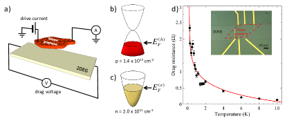
To further investigate this effect we explore a second device comprising of a hole-doped exfoliated BLG deposited on the surface of a GaAs quantum heterostructure. The hole density in BLG is from the low-field (below ) classical Hall effect and the mobility is at . The 2DEG has an electron density and a mobility at . Contrary to the SLG/2DEG case, in the BLG/2DEG device both electron and hole fluids have parabolic energy-momentum dispersions, Figs. 4b)-c), recently predicted perali_prl_2013 to be particularly favorable for the occurrence of e-h pairing. Since e-h pairing stems from e-e interactions, a lower kinetic energy in BLG (vanishing like andre_naturemater_2007 rather than like for small values of momentum ) compared to SLG enhances the relative importance of Coulomb interactions Giuliani_and_Vignale in BLG/2DEG heterostructures. To probe this, we measure the evolution of as a function of using BLG as the drive layer. Fig. 4 again shows a significant departure from the Fermi-liquid dependence. Consistent with the expected larger impact of interactions perali_prl_2013 ; Giuliani_and_Vignale , we get , i.e. twice the SLG/2DEG case, while the best fit of data based on Eq. (1) yields (to be compared with - in the SLG/2DEG).
A possible approach to further increase and is to tune the electron and hole densities in the two layers in such a way to match the corresponding Fermi wave numbers, and , respectively. In our devices the mismatch in the Fermi wave numbers is in the SLG/2DEG and in the BLG/2DEG case. Such a mismatch is expected pieri_prb_2007 to weaken the robustness of the exciton condensate phase in which condensed e-h pairs have zero total momentum . Preliminary calculations perali_private_commun , which include screening in the condensed phase sodemann_prb_2012 ; lozovik_prb_2012 ; neilson_arxiv_2013 , indicate that the exciton condensate state persists even in the presence of these values of , with scales comparable to those reported here. On the other hand, a mismatch in the Fermi wave numbers of the two fluids may favor other superfluid states, such as those discussed in Refs. fulde_pr_1964, ; larkin_jept_1965, ; casalbuoni_rmp_2004, ; pieri_prb_2007, ; subasi_prb_2010, . These states are however rather fragile in dimensionality , although some evidence was reported, e.g., in the layered heavy-fermion superconductor bianchi_prl_2003 .
The topic of exciton condensation is at the front-end of current condensed-matter research and it involves experimental studies of a wide class of solid-state systems rontani . Those include exciton-polaritons in semiconductor microcavities Kasprzak , which however display ultrashort (picosecond) lifetimes and optically-created indirect excitons in asymmetric semiconductor double quantum wells, where condensation competes with diffusion of the photo-created electrons and holes butov . Condensation of permanent inter-layer excitons was instead demonstrated in electron-electron double layers but at the price of applying high (several Tesla) magnetic fields to enter the quantum Hall regime (see Ref. nandi_nature_2012, and references therein). Finally, upturns of the Coulomb drag resistivity were reported in e-h doped GaAs/AlGaAs coupled quantum wells croxall_prl_2008 ; seamons_prl_2009 ; morath_prb_2009 . However, the combination of 2d electron and hole gases in the same GaAs material required a large nanofabrication effort and the reported magnitude of the drag anomalies was smaller than that found in our hybrid heterostructures. Thus our observations establish a new class of vertical heterostructure devices with a potentially large flexibility in the design of band dispersions, doping, and e-h coupling where excitonic phenomena are easily accessible.
Systems of inter-layer excitons might be used to create coherent interconnections between electronic signal processing and optical communication in integrated circuits high_science_2008 ; kuznetsova_opticsletters_2010 ; sanvitto_naturecommun_2013 or interfaced with superconducting contacts for a variety of applications, including analog-to-digital converters dolcini_prl_2010 and topologically protected quantum bits peotta_prb_2011 . The latter devices require, however, the exploitation of InAs-based 2DEGs that, unlike GaAs, make very good contact (i.e. no Schottky barriers) to superconductors deon_apl_2011 . Inter-layer excitons in graphene/InAs hybrids may also pave the way for the exploration of the interplay between spin-orbit coupling and pairing fluctuations.
Acknowledgements.
We thank R. Duine, R. Fazio, A. Hamilton, M. Katsnelson, A. MacDonald, D. Neilson, K. Novoselov, A. Perali, A. Pinczuk, and G. Vignale for very useful discussions. We acknowledge funding from EU Graphene Flagship (contract no. CNECT-ICT-604391), EC ITN project “INDEX” Grant No. FP7-2011-289968, the Italian Ministry of Education, University, and Research (MIUR) through the program “FIRB - Futuro in Ricerca 2010” Grant No. RBFR10M5BT (“PLASMOGRAPH”), ERC grants NANOPOTS, Hetero2D, a Royal Society Wolfson Research Merit Award, EU projects GENIUS, CARERAMM, RODIN, EPSRC grants EP/K01711X/1, and EP/K017144/1.Appendix A Sample details and fabrication
The samples are modulation-doped GaAs/AlGaAs heterostructures hosting a 2DEG with single-layer (SLG) and bilayer graphene (BLG) flakes transferred onto them. Two different heterostructures (A and B) are investigated, differing only in the width of the quantum well, which lies from the surface in both cases. The layer sequence, Fig. 5a), starting from the surface comprises a -thick -doped GaAs cap layer, followed by a undoped GaAs and a -thick undoped barrier layer of . The GaAs quantum well has a thickness of in sample A and in sample B; it is followed by a thick barrier, which hosts a Si -doping located from the well. The two samples differ in carrier density and mobility, as reported in the main text.
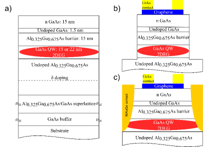
The Hall bar devices ( wide and long) are fabricated by UV lithography. Ni/AuGe/Ni/Au metals are evaporated and annealed at to form Ohmic contacts to the 2DEG. The mesa is then defined by wet etching in acid solution.
SLG and BLG flakes are produced by micromechanical exfoliation kostya_pnas_2005 of graphite on on Si substrates. The number of layers is identified by a combination of optical microscopy cnano and Raman spectroscopy RamanACF ; RamanACF2 . The latter is also used to monitor the sample quality by measuring the D to G ratio cancado and the doping level das . Selected flakes are then placed onto a GaAs-based substrate at the center of a pre-patterned Hall bar by using a polymer-based wet transfer process bonaccorso_matertoday_2012 . PMMA (molecular weight 950K) is first spin coated onto the substrate with micromechanically cleaved flakes, then the sample is immersed in de-ionized water, resulting in the detachment of the polymer film because of water intercalation at the PMMA-SiO2 interface bonaccorso_matertoday_2012 . Graphene flakes attach to the polymer and are removed from the substrate. The polymer+graphene film is then placed onto the target substrate and, after complete drying of the water, PMMA is removed by acetone. Success of the transfer is confirmed by optical inspection (bright and dark field microscopy), atomic force microscopy (AFM) and Raman spectroscopy. Raman spectra are collected with a Renishaw InVia spectrometer using laser excitation wavelengths at . Excitation power is kept below to avoid local heating and the scattered light is collected with a 100X objective. Fig. 6 plots the spectra of SLG and BLG flakes before and after transfer.
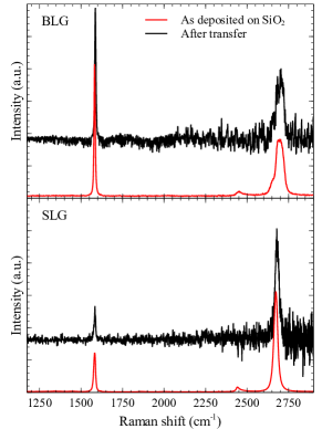
The strong luminescence background due to the GaAs/AlGaAs substrate has been subtracted out in order to highlight the Raman signal of the SLG/BLG flakes after transfer. This, combined with the lack of interference enhancement on the GaAs/AlGaAs substrate, explains why the spectra of the transferred flakes are noisy. As discussed in the main text for the SLG flake, also for the BLG flake we do not see any increase of D peak, thus showing that the transfer procedure does not induce extra defects.
Since the flakes are much smaller than the Hall bar widths, in each device we define a narrow channel () in the Hall bar by electron beam lithography (EBL) and wet etching, see Figs. 5b)-c). To avoid exposure of the flakes to the electron beam, we took an optical image to align the EBL. This procedure is possible because SLG and BLG on this substrate become optically visible once coated by PMMA, see Fig. 1. Finally, Ohmic contacts (Cr/Au) are fabricated by EBL, metal evaporation and lift-off.
Appendix B Electrical characterization
As described in the main text, the anomalous quantum Hall effect (QHE) in SLG is seen at when the 2DEG is not induced in the GaAs channel (see also black curve in Fig. 7). A markedly different result is seen when the 2DEG is induced by LED illumination. This is shown in Fig. 7, where we compare the Hall resistance at as a function of the perpendicular magnetic field up to for the two cases.
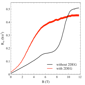
Because of the massless Dirac fermion nature of the charge carriers in SLG and the spin-valley degeneracy, plateaus are expected castroneto_rmp_2009 in the Hall resistance at , with . When the 2DEG is not induced, QHE plateaus are visible at while, as expected, the plateau is missing. In the other case, the plateau at is not visible and the resistance approaches the value for at the highest magnetic field. The two configurations have different mobility, , without the 2DEG, with the 2DEG. As explained in the main text, we can explain this difference considering that charged impurities (ionized Si donors) are left in the heterostructure when the 2DEG is induced, resulting in turn in an enhanced scattering of SLG carriers, which reduces mobility dassarma_rmp_2011 .
Appendix C Inter-layer (“leakage”) current
Measurements of the leakage current between the two layers are performed by applying a voltage source to the 2DEG and detecting the current with an ammeter connected to SLG/BLG Gupta . The applied voltage is negative to avoid depletion of the 2DEG.
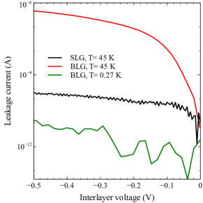
We report in Fig. 8 the measured leakage currents for the SLG and BLG devices as a function of the inter-layer voltage. We recall that in the drag experiment configuration, the maximum negative value for this voltage is . In the case of SLG, the current is smaller than even at . In the case of BLG we find a larger current at , but still much smaller than the drive current measured in the drag experiment (in the worst case of we have a leakage current of while the drive current is ). At the lowest temperature, the leakage current in BLG is smaller than the drive current by many orders of magnitude, so we do not expect it to affect the drag measurement gorbachev_naturephys_2012 .
Appendix D Drag measured by using graphene as a passive layer
The temperature dependence of in SLG as a function of the drive current in the 2DEG is reported in Fig. 9a). Upon reducing temperature, the drag voltage measured in SLG displays a series of oscillations, which we believe to be linked to mesoscopic fluctuations already discussed in Coulomb drag setups based on two spatially-separated SLG sheets gorbachev_naturephys_2012 ; kim_prb_2011 ; kim_ssc_2012 and also for all GaAs/AlGaAs double layers price_science_2007 . These fluctuations disappear for . Above this temperature the - relation becomes linear.
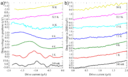
When the voltage drop is measured in the 2DEG no fluctuations arise at all the explored temperatures: see Fig. 9b). This allows us to extract the evolution of the drag resistance down to (see main text). A similar fluctuating behaviour of the drag voltage at low temperature is found in sample B in the configuration in which BLG is used as the passive layer.
Appendix E Theoretical background
We summarize the most elementary theory of drag resistance in the Fermi-liquid regime rojo_jpcm_1999 , which is based on Boltzmann-transport theory supplemented by second-order perturbation theory in the screened inter-layer interaction rojo_jpcm_1999 .
In the SLG/2DEG vertical heterostructure, the drag resistivity is given, in the low-temperature limit, by principi_prb_2012 :
| (2) | |||||
where () is the Fermi velocity in the top (bottom) layer, () is the Fermi energy in the top (bottom) layer, () is the Fermi wave number in the top (bottom) layer, , and . The low-temperature limit is defined by the inequality .
In Eq. (2) the screened interaction is given by:
| (3) |
where
| (4) | |||||
is the dielectric function in the random phase approximation Giuliani_and_Vignale . In Eq. (4), and are the density-density linear response functions of the electronic fluids in the top and bottom layer, respectively. Microscopic expressions for the density-density response function of the electron fluid in a doped graphene sheet can be found in Refs. wunsch_njp_2006, ; hwang_prb_2007, ; barlas_prl_2007, . The density-density response function of a 2DEG is extensively discussed in Ref. Giuliani_and_Vignale, .
In Eqs. (3)-(4), is the Coulomb interaction between two charges in the top layer,
| (5) |
while is the Coulomb interaction in the bottom layer,
| (6) |
with . Finally, the inter-layer interaction is given by
| (7) |
The dimensionless parameter represents the relative dielectric constant of the material above SLG (in our case air, ), while is the relative dielectric constant of GaAs, which is . In writing Eqs. (5)-(7) we neglect the difference between the dielectric constant of GaAs and AlGaAs. Note that in Eqs. (5)-(7) we introduced a form factor , which stems from the finite width of the quantum well hosting the 2DEG. This can be found davies by solving the Poisson equation for the SLG/2DEG vertical heterostructure under the assumption that the confining potential for the 2DEG along the growth direction is given by a square quantum well of width . This assumption has been checked with the help of a self-consistent Poisson-Schrödinger solver. We find
| (8) |
References
- (1) Novoselov, K. S. & Castro Neto, A. H. Two-dimensional crystals-based heterostructures: materials with tailored properties. Phys. Scr. T146, 014006 (2012).
- (2) Bonaccorso, F., Lombardo, A., Hasan, T., Sun, Z., Colombo, L. & Ferrari, A. C. Production and processing of graphene and 2d crystals. Mater. Today 15, 564 (2012).
- (3) Britnell, L., Gorbachev, R. V., Jalil, R., Belle, B. D., Schedin, F., Mishchenko, A., Georgiou, T., Katsnelson, M. I., Eaves, L., Morozov, S. V., Peres, N. M. R., Leist, J., Geim, A. K., Novoselov, K. S. & Ponomarenko, L. A. Field-effect tunneling transistor based on vertical graphene heterostructures. Science 335, 947-950 (2012).
- (4) Ponomarenko, L. A., Geim, A. K., Zhukov, A. A., Jalil, R., Morozov, S. V., Novoselov, K. S., Grigorieva, I. V., Hill, E. H., Cheianov, V. V., Fal’ko, V. I., Watanabe, K., Taniguchi, T. & Gorbachev, R. V. Tunable metal-insulator transition in double-layer graphene heterostructures. Nature Phys. 7, 958-961 (2011).
- (5) Kim, S., Jo, I., Nah, J., Yao, Z., Banerjee, S. K. & Tutuc, E. Coulomb drag of massless fermions in graphene. Phys. Rev. B 83, 161401(R) (2011).
- (6) Gorbachev, R. V., Geim, A. K., Katsnelson, M. I., Novoselov, K. S., Tudorovskiy, T. Grigorieva, I. V., MacDonald, A. H., Morozov, S. V., Watanabe, K., Taniguchi, T. & Ponomarenko, L. A. Strong Coulomb drag and broken symmetry in double-layer graphene. Nature Phys. 8, 896-901 (2012).
- (7) Kim, S. & Tutuc, E. Coulomb drag and magnetotransport in graphene double layers. Solid State Commun. 152, 1283 (2012).
- (8) Geim, A. K. & Novoselov, K. S. The rise of graphene. Nature Mater. 6, 183-191 (2007).
- (9) High, A. A., Novitskaya, E. E., Butov, L. V. & Gossard, A. C. Control of exciton fluxes in an excitonic integrated circuit. Science 321, 229-231 (2008).
- (10) Kuznetsova, Y. Y., Remeika, M., High, A. A., Hammack, A. T., Butov, L. V., Hanson, M. & Gossard, A. C. All-optical excitonic transistor. Optics Lett. 35, 1587-1589 (2010).
- (11) Ballarini, D., De Giorgi, M., Cancellieri, E., Houdré, R., Giacobino, E., Cingolani, R., Bramati, A., Gigli, G. & Sanvitto, D. All-optical polariton transistor. Nature Comm. 4, 1778 (2013).
- (12) Dolcini, F., Rainis, D., Taddei, F., Polini, M., Fazio, R. & MacDonald, A. H. Blockade and counterflow supercurrent in exciton-condensate Josephson junctions. Phys. Rev. Lett. 104, 027004 (2010).
- (13) Peotta, S., Gibertini, M., Dolcini, F., Taddei, F., Polini, M., Ioffe, L. B., Fazio, R. & MacDonald, A. H. Josephson current in a four-terminal superconductor/exciton-condensate/superconductor system. Phys. Rev. B 84, 184528 (2011).
- (14) Novoselov, K. S., Jiang, D., Schedin, F., Booth, T. J., Khotkevich, V. V., Morozov, S. V. & Geim, A. K. Proc. Natl. Acad. Sci. (USA) 102, 10451-10453 (2005).
- (15) Casiraghi, C., Hartschuh, A., Lidorikis, E., Qian, H., Harutyunyan, H., Gokus, T., Novoselov, K. S. & Ferrari, A. C. Rayleigh imaging of graphene and graphene layers. Nano Lett. 7, 2711-2717 (2007).
- (16) Ferrari, A. C., Meyer, J. C., Scardaci, V., Casiraghi, C., Lazzeri, M., Mauri, F., Piscanec, S., Jiang, D., Novoselov, K. S., Roth, S. & Geim, A. K. Raman spectrum of graphene and graphene layers. Phys. Rev. Lett. 97, 187401 (2006).
- (17) Ferrari, A. C. & Basko, D. M. Raman spectroscopy as a versatile tool for studying the properties of graphene. Nature Nanotech. 8, 235-246 (2013).
- (18) Cancado, L. G., Jorio, A., Martins Ferreira, E. H., Stavale, F., Achete, C.A., Capaz, R. B., Moutinho, M. V. O., Lombardo, A., Kulmala, T. & Ferrari, A. C. Quantifying defects in graphene via Raman spectroscopy at different excitation energies. Nano Lett. 11, 3190-3196 (2011).
- (19) Das, A., Pisana, S., Piscanec, S., Chakraborty, B., Saha, S. K., Waghmare, U. V., Yang, R., Novoselov, K.S., Krishnamurhthy, H. R., Geim, A. K., Ferrari, A. C. & Sood, A. K. Monitoring dopants by Raman scattering in an electrochemically top-gated graphene transistor. Nature Nanotech. 3, 210-215 (2008).
- (20) Pfeiffer, L. N. and West, K. W. The role of MBE in recent quantum Hall effect physics discoveries. Physica E 20, 57-64 (2003).
- (21) Basko, D. M., Piscanec, S. & Ferrari, A. C. Electron-electron interactions and doping dependence of the two-phonon Raman intensity in graphene. Phys. Rev. B 80, 165413 (2009).
- (22) Gramila, T. J., Eisenstein, J. P., MacDonald, A. H., Pfeiffer, L. N. & West, K. W. Mutual friction between parallel two-dimensional electron systems. Phys. Rev. Lett. 66, 1216-1219 (1991).
- (23) Sivan, U., Solomon, P. M. & Shtrikman, H. Coupled electron-hole transport. Phys. Rev. Lett. 68, 1196-1199 (1992).
- (24) Rojo, A. G. Electron-drag effects in coupled electron systems. J. Phys.: Condens. Matter 11, R31 (1999).
- (25) Zheng, L. & MacDonald, A. H. Coulomb drag between disordered two-dimensional electron-gas layers. Phys. Rev. B 48, 8203-8209 (1993).
- (26) Kamenev, A. & Oreg, Y. Coulomb drag in normal metals and superconductors: Diagrammatic approach. Phys. Rev. B 52, 7516-7527 (1995).
- (27) Giordano, N. & Monnier, J. D. Cross-talk effects in superconductor-insulator-normal-metal trilayers. Phys. Rev. B 50, 9363-9368 (1994).
- (28) Pillarisetty, R., Noh, H., Tutuc, E., De Poortere, E. P., Lai, K., Tsui, D. C. & Shayegan, M. Coulomb drag near the metal-insulator transition in two dimensions. Phys. Rev. B 71, 115307 (2005).
- (29) Yamamoto, M., Stopa, M., Tokura, Y., Hirayama, Y. & Tarucha, S. Negative Coulomb drag in a one-dimensional wire. Science 313, 204-207 (2006).
- (30) Nandi, D., Finck, A. D. K., Eisenstein, J. P., Pfeiffer, L. N. & West, K. W. Exciton condensation and perfect Coulomb drag. Nature 488, 481-484 (2012).
- (31) Vignale, G. & MacDonald, A. H. Drag in paired electron-hole layers. Phys. Rev. Lett. 76, 2786-2789 (1996).
- (32) Hu, B. Y.-K. Prospecting for the superfluid transition in electron-hole coupled quantum wells using Coulomb drag. Phys. Rev. Lett. 85, 820-823 (2000).
- (33) Snoke, D. Spontaneous Bose coherence of excitons and polaritons. Science 298, 1368-1372 (2002).
- (34) Mink, M. P., Stoof, H. T. C., Duine, R. A., Polini, M. & Vignale, G. Probing the topological exciton condensate via Coulomb drag. Phys. Rev. Lett. 108, 186402 (2012).
- (35) Mink, M. P., Stoof, H. T. C., Duine, R. A., Polini, M. & Vignale, G. Unified Boltzmann transport theory for the drag resistivity close to an interlayer-interaction-driven second-order phase transition. Phys. Rev. B 88, 235311 (2013).
- (36) Larkin, A. & Varlamov, A. Theory of Fluctuations in Superconductors (Clarendon Press, Oxford, 2004).
- (37) Prange, R. E. & Girvin, S. M. The Quantum Hall Effect (Springer-Verlag, New York, 1990).
- (38) Das Sarma, S., Adam, S., Hwang, E. H. & Rossi, E. Electronic transport in two-dimensional graphene. Rev. Mod. Phys. 83, 407-470 (2011).
- (39) Carrega, M., Tudorovskiy, T., Principi, A., Katsnelson, M. I. & Polini, M. Theory of Coulomb drag for massless Dirac fermions. New J. Phys. 14, 063033 (2012).
- (40) Principi, A., Carrega, M., Asgari, R., Pellegrini, V. & Polini, M. Plasmons and Coulomb drag in Dirac/Schrödinger hybrid electron systems. Phys. Rev. B 86, 085421 (2012).
- (41) Onsager, L. Reciprocal relations in irreversible processes. I. Phys. Rev. 37, 405-426 (1931).
- (42) Onsager, L. Reciprocal relations in irreversible processes. II. Phys. Rev. 38, 2265-2279 (1931).
- (43) E.g., fixing , the best fit yields and . We can well fit the experimental data by choosing any value of , as long as this is substantially lower than the lowest investigated temperature, i.e. . As it is clear from the functional form of the fitting function in Eq. (1), in this regime a change can be reabsorbed into a change of the background resistance .
- (44) Rist, S., Varlamov, A. A., MacDonald, A. H., Fazio, R. & Polini, M. Photoemission spectra of massless Dirac fermions on the verge of exciton condensation. Phys. Rev. B 87, 075418 (2013).
- (45) Zhang, W., Smallwood, C. L., Jozwiak, C., Miller, T. L., Yoshida, Y., Eisaki, H., Lee, D.-H. & Lanzara, A. Signatures of superconductivity and pseudogap formation in nonequilibrium nodal quasiparticles revealed by ultrafast angle-resolved photoemission. Phys. Rev. B 88, 245132 (2013).
- (46) Feld, M., Fröhlich, B., Vogt, E., Koschorreck, M. & Köhl, M. Observation of a pairing pseudogap in a two-dimensional Fermi gas. Nature 480, 75-78 (2011).
- (47) Perali, A., Neilson, D. & Hamilton, A. R. High-temperature superfluidity in double-bilayer graphene. Phys. Rev. Lett. 110, 146803 (2013).
- (48) Giuliani, G. F. & Vignale, G. Quantum Theory of the Electron Liquid (Cambridge University Press, Cambridge, 2005).
- (49) Pieri, P., Neilson, D. & Strinati, G. C. Effects of density imbalance on the BCS-BEC crossover in semiconductor electron-hole bilayers. Phys. Rev. B 75, 113301 (2007).
- (50) Perali, A. & Neilson, D., private communication.
- (51) Sodemann, I., Pesin, D. A. & MacDonald, A. H. Interaction-enhanced coherence between two-dimensional Dirac layers. Phys. Rev. B 85, 195136 (2012).
- (52) Lozovik, Yu. E., Ogarkov, S. L. & Sokolik, A. A. Condensation of electron-hole pairs in a two-layer graphene system: correlation effects. Phys. Rev. B 86, 045429 (2012).
- (53) Neilson, D., Perali, A., & Hamilton, A. R. Excitonic superfluidity and screening in electron-hole bilayer systems. arXiv:1308.0280.
- (54) Fulde, P. & Ferrell, R. A. Superconductivity in a strong spin-exchange field. Phys. Rev. 135, A550-A563 (1964).
- (55) Larkin A. J. & Ovchinnikov, Y. N. Inhomogeneous state of superconductors. Sov. Phys. JEPT 20, 762 (1965).
- (56) Casalbuoni, R. & Nardulli, G. Inhomogeneous superconductivity in condensed matter and QCD. Rev. Mod. Phys. 76, 263-320 (2004).
- (57) Subaşı, A. L., Pieri, P., Senatore, G. & Tanatar, B. Stability of Sarma phases in density imbalanced electron-hole bilayer systems. Phys. Rev. B 81, 075436 (2010).
- (58) Bianchi, A., Movshovich, R., Capan, C., Pagliuso, P. G. & Sarrao, J. L. Possible Fulde-Ferrell-Larkin-Ovchinnikov superconducting state in . Phys. Rev. Lett. 91, 187004 (2003).
- (59) For a recent review see, e.g., Rontani, M. & Sham, L. J. Coherent exciton transport in semiconductors. Novel Superfluids Vol. 2, edited by Bennemann, K. H. & Ketterson, J. B., International Series of Monographs on Physics no. 157 (Oxford University Press). Also available as arXiv:1301.1726.
- (60) Kasprzak, J., Richard, M., Kundermann, S., Baas, A., Jeambrun, P., Keeling, J. M. J., Marchetti, F. M., Szymańska, M. H., André, R., Staehli, J. L., Savona, V., Littlewood, P. B., Deveaud, B. & Dang, Le Si Bose-Einstein condensation of exciton polaritons. Nature 443, 409-414 (2006).
- (61) High, A. A., Leonard, J. R., Hammack, A. T., Fogler, M. M., Butov, L. V., Kavokin, A. V., Campman K. L., & Gossard A. C. Spontaneous coherence in a cold exciton gas. Nature 483, 584-588 (2012).
- (62) Croxall, A. F., Das Gupta, K., Nicoll, C. A., Thangaraj, M., Beere, H. E., Farrer, I., Ritchie, D. A. & Pepper, M. Anomalous Coulomb drag in electron-hole bilayers. Phys. Rev. Lett. 101, 246801 (2008).
- (63) Seamons, J. A., Morath, C. P., Reno, J. L., & Lilly, M. P. Coulomb drag in the exciton regime in electron-hole bilayers. Phys. Rev. Lett. 102, 026804 (2009).
- (64) Morath, C. P., Seamons, J. A., Reno, J. L., & Lilly, M. P. Density imbalance effect on the Coulomb drag upturn in an undoped electron-hole bilayer. Phys. Rev. B 79, 041305(R) (2009).
- (65) See, e.g., Deon, F., Pellegrini, V., Giazotto, F., Biasiol, G., Sorba, L. & Beltram, F. Quantum dot spectroscopy of proximity-induced superconductivity in a two-dimensional electron gas. Appl. Phys. Lett. 98, 132101 (2011).
- (66) Castro Neto, A. H., Guinea, F., Peres, N. M. R., Novoselov, K. S. & Geim, A. K. The electronic properties of graphene. Rev. Mod. Phys. 81, 109 (2009).
- (67) Das Gupta, L., Croxall, A. F., Waldie, J., Nicoll, C. A., Beere, H. E., Farrer, I., Ritchie, D. A. & Pepper, M. Experimental progress towards probing the ground state of an electron-hole bilayer by low-temperature transport. Advances in Condensed Matter Physics 2011, 1-22 (2011).
- (68) Price, A. S., Savchenko, A. K., Narozhny, B. N., Allison, G. & Ritchie, D. A. Giant fluctuations of Coulomb drag in a bilayer system. Science 316, 99-102 (2007).
- (69) Wunsch, B., Stauber, T., Sols, F. & Guinea, F. Dynamical polarization of graphene at finite doping. New J. Phys. 8, 318 (2006).
- (70) Hwang, E. H. & Das Sarma, S. Dielectric function, screening, and plasmons in two-dimensional graphene. Phys. Rev. B 75, 205418 (2007).
- (71) Barlas, Y., Pereg-Barnea, T., Polini, M., Asgari, R. & MacDonald, A. H. Chirality and correlations in graphene. Phys. Rev. Lett. 98, 236601 (2007).
- (72) Davies, J. The Physics of Low-dimensional Semiconductors (Cambridge University Press, Cambridge, 1998).