Electronic structure and magnetic properties of Mn and Fe impurities near GaAs (110) surface
Abstract
Combining density-functional theory calculations and microscopic tight-binding models, we investigate theoretically the electronic and magnetic properties of individual substitutional transition-metal impurities (Mn and Fe) positioned in the vicinity of the (110) surface of GaAs. For the case of the plus acceptor-hole (h) complex, the results of a tight-binding model including explicitly the impurity -electrons are in good agreement with approaches that treat the spin of the impurity as an effective classical vector. For the case of Fe, where both the neutral isoelectronic and the ionized states are relevant to address scanning tunneling microscopy (STM) experiments, the inclusion of -orbitals is essential. We find that the in-gap electronic structure of Fe impurities is significantly modified by surface effects. For the neutral acceptor state , the magnetic-anisotropy dependence on the impurity sublayer resembles the case of . In contrast, for electronic configuration the magnetic anisotropy behaves differently and it is considerably smaller. For this state we predict that it is possible to manipulate the Fe moment, e.g. by an external magnetic field, with detectable consequences in the local density of states probed by STM.
pacs:
75.50.Pp, 71.55.Eq, 71.15.MbI INTRODUCTION:
The study of the spin of individual transition-metal (TM) dopants in
a semiconductor host is an emergent field known as magnetic solotronics,
bearing exciting prospects for novel spintronics devices at the atomic
scale. Koenraad and Flatté (2011) The development of scanning tunneling microscopy
(STM) based techniques enabled the investigation of substitutional dopants
at a semiconductor surface with unprecedented accuracy and
degree of details. Yakunin et al. (2004); Shinada et al. (2005); Kitchen et al. (2006); Marczinowski et al. (2007); Lee and Gupta (2010); Garleff et al. (2010); Fuechsle et al. (2012); Pla et al. (2012)
The experimental advances have stimulated
theoretical studies of individual
magnetic impurities in semiconductors, based both on first-principles
calculations Zhao et al. (2004); Mahadevan et al. (2004); Mikkelsen et al. (2004); Stroppa et al. (2007); Ebert and Mankovsky (2009); Islam and Canali (2012)
and microscopic tight-binding (TB)
models. Tang and Flatté (2004, 2005); Timm and MacDonald (2005); Jancu et al. (2008); Strandberg et al. (2009, 2010, 2011); Mašek et al. (2010); Bozkurt et al. (2013)
Approaches based on the TB models
are particularly convenient to explore the solotronics limit of dilute
impurities in semiconductor hosts.
For the specific case of Mn dopants on the (110) GaAs surface,
TB models Tang and Flatté (2004, 2005); Jancu et al. (2008); Strandberg et al. (2009, 2010, 2011); Bozkurt et al. (2013)
have provided a quantitative description of the
electronic and magnetic properties of the associated acceptor states.
Early work by Tang and Flatté Tang and Flatté (2004) introduced
a TB model for a single substitutional Mn impurity in bulk GaAs.
Here the electronic structure of the host is described by a TB Hamiltonian, while
the hybridization between the Mn -levels and the -levels
of the nearest neighbors As atoms is
modeled as an effective spin-dependent potential.
This model captures several of the key features
of the Mn acceptor physics in GaAs found in experiment,
such as the anisotropic shape of the Mn
acceptor wavefunction.
However, the inclusion of surface effects are expected to be important for
a direct comparison with STM experiments,
where accessible impurities
are positioned in the proximity of the surface.
Later experimental Garleff et al. (2008)
and theoretical Jancu et al. (2008); Strandberg et al. (2009) studies
have indeed demonstrated a strong influence of the surface
on the properties of the Mn acceptor state.
In particular, the electronic structure and magnetic properties
of Mn on the (110) GaAs surface and in near-surface
layers have been investigated theoretically
in Ref. Strandberg et al., 2009.
This work uses a finite-cluster sp3 TB model for GaAs,
with the Mn impurity spin introduced as a classical spin, exchange-coupled
to the quantum spins of the nearest-neighbor As atoms.
For a substitutional Mn in bulk GaAs this model
is in good agreement with Ref. Tang and Flatté, 2004.
For a Mn on the surface the model finds, in agreement with
experimentKitchen et al. (2006); Lee and Gupta (2010),
a strongly localized and anisotropic mid-gap acceptor state.
Furthermore, the model makes predictions on the dependence of the
acceptor binding energy and magnetic anisotropy energy
on the subsurface layer where the Mn is positioned.
The former result has been later confirmed experimentally. Garleff et al. (2010)
The theoretical approach used both in Ref. Tang and Flatté, 2004
and Ref. Strandberg et al., 2009
must be viewed as an effective spin model for the Mn spin,
where the Mn -levels have been integrated out
and the Mn spin is treated as a classical vector.
The fact that this effective model
makes predictions consistent with experiment, and
it also agrees with TB approaches retaining a microscopic
description of -levels Jancu et al. (2008),
is a strong indication that the effective classical-spin approach
is essentially correct for a Mn impurity in GaAs, characterized by a half-filled -shell.
The model does have some limitations, which are recognized and
understood. Bozkurt et al. (2013)
Other TM impurities in GaAs are less investigated and understood,
and more refined microscopic theories are necessary.
This is one of the motivations of the present work.
The need of a microscopic description of TM impurities
on a semiconductor surface is also motivated by recent STM experimental studies
of Fe dopants on the (110) surface of GaAs. Richardella et al. (2009); Bocquel et al. (2013); Mühlenberend et al. (2013)
Despite similarities in the STM topographies of Mn and Fe impurities
as a result of the underlying symmetry of the host material Richardella et al. (2009), the
electronic structures of Mn and Fe ions within the GaAs gap
are known to be
different Mn Malguth1 et al. (2008), and this should have consequences in the STM
spectroscopic features.
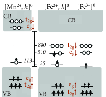
This can already be seen in Fig. 1, where we draw
schematically possible electronic configurations of Mn and Fe ions in bulk GaAs.
In fact, two experimental groups have reported
somewhat different results in the details of the Fe impurity-induced
in-gap electronic structure probed by STM.
Richardella et al. Richardella et al. (2009)
found two impurity-induced peaks in their spectroscopic measurements,
while a more recent study reported several peaks
below and above the valence band maximum, which can be associated
with the Fe impurity. Mühlenberend et al. (2013)
Another aspect of the complex electronic structure of Fe dopants on the (110)
surface of GaAs has been investigated
in the STM experiments by Bocquel et al. Bocquel et al. (2013)
The authors demonstrated the possibility of manipulating
the -shell occupancy of Fe via a voltage-dependent local manipulation
of the Fermi level due to tip-induced band bending.
In particular, a transition from an isoelectronic
to an ionized acceptor state (see Fig. 1) was realized
by varying the tip voltage. This transition corresponds to the
change in the filling of the impurity -shell from
five () to six () electrons and therefore to the change
in the core spin state from to .
It is clear that the classical-spin model, used to described
the neutral plus acceptor-hole (h) complex (),
is not applicable in this case, as it can not account
for the change in the valence state of Fe.
In this paper we employ a combined approach using both density functional
theory (DFT) calculations and microscopic TB modeling to
study the electronic structure and magnetic properties of substitutional
Mn and Fe impurities on the (110) GaAs surface and up to
nine monolayers below the surface. In our TB model we include explicitly
the -, - and -orbitals of the impurity atom.
The relative shifts in the on-site energies for the exchange-split minority and
majority -levels of the dopant are extracted from DFT calculations.
For the case of Mn we find good agreement
with previous work, where the Mn magnetic moments was treated classically. This indicates that
our microscopic TB model correctly reproduces the physics of the complex,
while providing access to additional features inaccessible by the classical spin-model.
In the case of Fe, we perform
DFT calculations for both bulk and (110) GaAs surface. Here our DFT calculations provide a very valuable input for understanding
the changes in the in-gap electronic states due to the proximity to the surface,
and for interpreting the results of recent STM experiments.
Furthermore, using the TB model combined with parameters extracted directly from DFT calculations,
we provide a detailed analysis of the relevant electronic and magnetic properties of Fe on the (110) GaAs surface.
In particular, we calculate
the spatial distribution of the wavefunctions associated with the impurity-induced states
in the gap as well as the magnetic anisotropy and its
dependence on the valence state of the impurity. We show that for the neutral acceptor state ,
the magnetic-anisotropy dependence on the impurity position with respect to the surface layer
is similar to that of .
In contrast to this, the isoelectronic state, ,
behaves differently and its anisotropy energy is considerably smaller. This result suggests a route towards manipulation
of the Fe magnetic moment by external magnetic fields,
accompanied by detectable changes in the electronic local density of states (LDOS) which can be measured by STM.
This is different from the case of Mn,
where such manipulation was shown to be difficult since the large magnetic anisotropy energy (up to 15meV)
of Mn in the subsurface layers would require
extremely strong magnetic fields to change the direction of its magnetic moment. Bozkurt et al. (2013)
The rest of the paper is organized as follows. In the next section
In Sec. II.
we describe the details of our microscopic TB approach.
In Sec. III we present the results of DFT calculations for Mn and Fe impurities in GaAs,
and discuss how these results can be used to extract
some of the parameters of the TB Hamiltonian.
The results of the TB calculations are described in section IV.
Firstly, in section IV.1 we present the calculations of the electronic energy spectrum, LDOS
and magnetic anisotropy for the Mn acceptor on the (110) GaAs surface and few layer below it. In particular, we provide a
quantitative comparison between the results obtained with our fully microscopic TB model
and the results of the classical spin model for Mn,
reported previously. Strandberg et al. (2009)
Secondly, in section IV.2 we address similar properties of Fe dopants both in bulk GaAs and on the (110)
GaAs surface. We focus in particular on the differences in the in-gap electronic structure,
LDOS and magnetic anisotropy, associated
with the Fe impurity in the bulk and on the surface. For the case of Fe on the surface, we show the dependence of the magnetic
anisotropy on the valence states of the impurity and discuss possible implications on
STM experiments. Finally, we draw some conclusions.
II MICROSCOPIC TIGHT-BINDING MODEL
We use a multi-orbital TB model to describe TM impurities substituting Ga atoms in GaAs.
The model includes - and -orbitals for all Ga and As atoms and -, - and -orbitals for
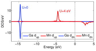
the impurity atoms. Introducing the -orbitals for the impurities only, and not for Ga atoms,
is justified by the fact that, as we will show in the next section,
the -levels of Ga are located far below ( 15 eV) the
Fermi level (see Fig. 4).
The second-quantized TB Hamiltonian for (Ga, TM)As takes the following form
| (1) |
The first term in Eq. (1) is the TB Hamiltonian for the GaAs host (with the exclusion of the Ga atoms replaced by the TM impurity). It is the sum of two terms
| (2) |
where
| (3) |
is the usual TB-band Hamiltonian for bulk GaAsChadi (1977) written in terms of Slater-Koster parameters, () Slater and Koster (1954); Papaconstantopoulos and Mehl (2003), representing both on-site energies and nearest-neighbors hopping amplitudes. Here and are electron creation and annihilation operators; and are atomic indices that run over all atoms other than the impurity, and are orbital indices and is a spin index defined with respect to an arbitrary quantization axis. The one-body term
| (4) |
models the on-site spin-orbit interaction (SOI) in GaAs, with the values of the re-normalized spin-orbit splittings taken from Ref. Chadi, 1977. The second term in Eq. (1) describes the TM impurity and its coupling to the atoms of the host. We have
| (5) |
where and are creation and annihilation operators
at the impurity site ; the orbital index runs over -, -, and -orbitals.
The first term in
Eq. (5) describes a hopping between the impurity and its As nearest-neighbors.
For the Slater-Koster hopping parameters between the impurity -orbitals and the nearest-neighbor
As - and -orbitals we use the same values as for the corresponding hopping parameters
between Ga and As, which are available in the literature. Jancu et al. (1998)
Our tight-binding model must be viewed as a phenomenological
approach which allows us to introduce, in a physically meaningful way,
the microscopic d-levels for the impurity and to go beyond the classical-spin model used previously.
The second term in Eq. (5) represents on-site energies of the impurity for a given orbital.
The -orbital energies play an important role in the model.
Their values for “spin-up” (majority)
and “spin-down” (minority) electrons
are different, which leads to a different occupation for opposite spin states,
and hence to a non-zero spin magnetic moment at the impurity site.
As a first estimate of the on-site -orbital energies, we use the values of the exchange-split
majority and minority -levels, which can be identified
in the spin- and orbital-resolved density of states (DOS) of the impurity, calculated with DFT.
The exact procedure and the choice of
the -orbital on-site energies for specific cases of Mn and Fe in GaAs will be discussed in
section III.
The last term in Eq. (5) is an on-site spin-orbit coupling term for the impurity atom,
analogous to the one given in Eq. (4).
The spin-orbit coupling terms and will cause the total
ground-state energy of the system
to depend on the direction of the impurity magnetic moment,
defined with respect to an arbitrary quantization axis. This is the origin of the magnetic anisotropy energy.
Finally, the third term in Eq. (1)
| (6) |
is a long-range repulsive Coulomb
potential that is dielectrically screened by the host material
(the index runs over all impurity atoms). This term prevents extra electrons from approaching
the impurity atom too
closely and therefore, prevents it from charging.
This contributes to localize the acceptor hole around the impurity.
The dielectric constant for the impurity on the GaAs
surface is reduced from the bulk GaAs value in order to mimic
a weaker dielectric screening at the surface (12 for bulk and 6 for the surface).
This crude choice is qualitatively supported by experimental results.Garleff et al. (2010)
As already mentioned in the introduction, the modeling of the TM impurity considered here (see Eq. 5)
differs from the approach of Ref. Strandberg et al., 2009
in that the TM impurity -orbitals are introduced explicitly.
In Ref. Strandberg et al., 2009
the -orbitals are integrated out and their spin-dependent hybridization with the As orbitals is represented by
the following effective spin Hamiltonian
| (7) |
Eq. 7 describes the antiferromagnetic exchange coupling (with coupling constant )
between the TM impurity spin
(treated as a classical vector) and the nearest neighbor
As -spins .
Below we will refer to the model of Eq. 7 as classical-spin model,
in contrast to the present impurity model,
given in Eq. 5, which will be denoted as quantum -level model.
The electronic structure of GaAs with a single substitutional Mn or Fe impurity atom
is obtained by performing supercell-type calculations with a cubic cluster of 3200 atoms
and periodic boundary conditions in either 2 or 3 dimensions, depending on
whether we are studying the surface or a bulk-like
system. The surface of GaAs is attractive from both
theoretical and experimental points of view due to the absence of large surface
reconstruction. In order to remove
artificial dangling-bond states that would otherwise appear in the
band gap, we include relaxation of surface layer positions
following a procedure put forward in
Refs. Chadi, 1978 and Chadi, 1979.
For more details the reader is
referred to Ref. Strandberg et al., 2009.
We would like to note here that while the effects of
strain induced by the (110) surface relaxation in GaAs are
included in our study, following the prescription of
Refs. Chadi, 1978 and Chadi, 1979 mentioned above, we do not take into
account the modification in strain and relaxation caused
by the presence of the magnetic impurity. A systematic study
of surface-induced strain and strain from an embedded quantum
dot on the symmetry of an acceptor is presented, respectively,
in Refs. Çelebi et al., 2010 and Yakunin et al., 2007.
In Ref. Niquet et al., 2009 the authors
present a model for the on-site matrix elements of the TB Hamiltonian
of a strained diamond or zinc-blend crystal.
Finally, in a more recent paper Zieliński (2012), the author
presents a method to include strain into the tight-binding Hamiltonian, which
is suitable for calculations of the electronic
and optical properties of semiconductor nanosystems
embedded in a host crystal. These extensions of the TB model represent future challenges to further improve the description of the strain effects induced by surfaces and impurities in semiconductors.
III DFT calculations and extraction of the TB parameters
The DFT calculations are performed using the full-potential all-electron method with
the basis consisting of linearized augmented plane waves combined with local orbitals (LAPW+lo),
as implemented
in the WIEN2k package. Blaha et al. (2001) We use the generalized gradient approximation (GGA) with
Perdew-Burke-Ernzerhof (PBE) exchange correlation functionalPerdew et al. (1996) as well as GGA+U, where the
orbital dependent parameter is used to capture electronic correlations
in the core shell of the impurity.
Because of the time-expensive nature of the plane wave method, we have used the SIESTA ab initio
package, which employs pseudopotentials and a numerical basis set Soler et al. (2002), for relaxing the
surfaces in our calculations. The relaxed coordinates are then used as input for WIEN2k calculations.
For bulk calculations, we consider a supercell containing a
total of 64 atoms, with one Ga atom replaced by a TM impurity atom. We use 100 non-equivalent
-points
in the Brillouin zone. For the surface calculations, a surface supercell with six layers,
each containing 16 atoms, is constructed by cleaving the bulk crystal along the direction. A vacuum
of 25 Bohr is added along the surface to avoid supercell interaction. All the surface calculations are
performed by substituting one Ga atom from the surface layer by a TM impurity. Note that due to computational
limitations caused by the large size of the supercell we use one k-point in the surface calculations. This
choice of k-point sampling can be justified based on the fact that the Brillouin zone for the surface
supercell is considerably smaller than that of the bulk. Islam and Canali (2012)
The DFT calculations carried out in this work
provide the spin-resolved DOS for the -electrons
of Mn and Fe impurities in the bulk and on the surface of GaAs. Importantly,
the splitting between the majority and the minority -levels of the impurities, calculated with DFT,
determines the relative values of the on-site energies for the corresponding
majority and minority -orbitals
in our TB model.
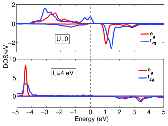
Fig. 2 shows the spin-resolved DOS for the
Mn dopant in bulk GaAs for two different choices of the parameter in the GGA+U calculations.
The parameter tends to localize the majority -shell electrons
and push them deeper in the valence band.
It is clear from the figure that the separation between
majority (spin-up) and minority (spin-down) -orbitals of different symmetry ( and )
increases with increasing the value of .
A microscopic determination of the parameter U
in first-principles GGA+U (or LDA+U) calculations in complex
materials is an outstanding and complicated issue in computational
physics and material science, details of which were first
addressed in Ref. Anisimov et al., 1991. For the specific
case of TM impurities in semiconductors, more information is
available on the value of U for Mn in GaAs via comparison with
experiment and calculations; while for the
case of Fe dopants, information is scarcer.
We believe that neglecting U altogether is
not justified, since some kind of self-interaction correction
to the TM must be included and it does have an effect on the
electronic structure, noticeably the position of the d-levels.
Our approach has been to choose a value not very different from
the value of U for Mn, under the assumption that the two cases should be
qualitatively similar and that small variations of U, if present,
should not change the results substantially.
Refs. Sato et al., 2010 and Belhadji et al., 2007
both use eV in Fe-doped GaN semiconductors.
In Ref. Gopal and Spaldin, 2006 which investigates several transition-metal-doped ZnO semiconductors
with LDA+U, the value of eV (and exchange eV) is used
for all transition metals. This paper mentions explicitly that,
although small variations are expected across the TM series, the
choice of constant values permits a more straightforward comparison,
which is precisely our point of view on this issue.
The value of is usually
chosen to match photoemission spectra
and in our calculation we use eV Sato et al. (2010),
although the results for are also presented.
The values of the on-site TB parameters for the Mn -orbitals in bulk
are determined based on the calculations with eV (see the bottom panel of Fig. 2).
As a first estimate for these parameters we take the positions of the spin-resolved and levels.
We then tune the value of the on-site energy for the majority orbital to get
the exact position of the acceptor level introduced by Mn in the bulk GaAs gap.
The values of the on-site energies are summarized in Table 1.
The spin-resolved DOS for Mn on the (110) GaAs surface is shown in Fig. 3.
The lower symmetry on the surface lifts the degeneracy of the -orbitals and,
strictly speaking, we can no longer identify peaks corresponding to orbitals with and
symmetry as in the bulk case. However, as one can see from the bottom panel
of Fig. 3, in the case of eV the positions of the main peaks in
the surface DOS are quantitatively similar to the positions of the and peaks
in the bulk calculation with the same value of U (bottom panel of Fig. 2).
Therefore, in our TB calculations for Mn on the (110) GaAs
surface we use the same set of parameters as for Mn in bulk.
As we will show in section IV.1,
the properties of the acceptor state obtained from these
calculations are in good agreement with the STM experiments.
| Mn (bulk) | Mn (surface) | Fe (bulk) | Fe (surface) | |
|---|---|---|---|---|
| -4.5 | -4.5 | -6.5 | -4.5 | |
| -2.226 | -2.226 | -6.5 | -4.5 | |
| 3.5 | 3.5 | -0.138 | -1 | |
| 3.5 | 3.5 | -0.02 | -1 |
In Fig. 4 we also plot the spin-resolved density of states for the -orbitals of a Ga atom on the (110) GaAs surface, and compare it with the analogous quantity for a substitutional Mn atom. We can clearly see that the Ga -orbitals are, as expected, unpolarized and occur at energies far below the Fermi level.
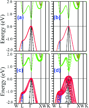
The band structure of bulk GaAs (see Fig. 5)
reveals that the top of the valence band in GaAs is completely
dominated by like states, both for Ga and As. Levels of
character are visibly present, particularly for Ga
atoms, even at the Gamma point. However, their contribution
is only 2% of the like states. These results justify our simplifying choice of
disregarding Ga -orbitals in the TB model.
We would like to emphasize that the level parameters in the empirical
TB model can differ considerably from the corresponding electronic atomic
orbitals. Therefore our remark on the position of the ab-initio Ga
level energy being far away from the Fermi energy as a
justification of our neglect of these levels in the TB model
must be taken with caution. Note, however, that the parametrization
of GaAs that we adopt here, which excludes levels of Ga and As atoms, is a
standard procedure and therefore the ab-initio results are not inconsistent
with neglecting the Ga and As levels in the TB model.
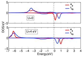
We will now discuss the case of Fe in GaAs. The spin-resolved DOS for the Fe dopant in
bulk GaAs is presented in Fig. 6. We note that our calculations
with for both Fe and Mn in bulk GaAs are in agreement with previously reported results. Mahadevan et al. (2004)
As one can see from Fig. 6,
the majority and peaks are pushed deeper in the valence band
for eV compared to the case with .
Interestingly, the positions of the minority and peaks above the Fermi level are sensitive to the value of U.
The minority doublet () level is lower in energy than the minority triplet ()
level for the case with , however these two levels swap for eV.
Based on the calculation with eV, we choose the positions of the
two main peaks for the majority -levels (-6.5 eV) as the on-site energy of the corresponding -orbitals
in our TB model for Fe in bulk.
We then tune the value of the on-site energy for the minority and orbitals to get
the exact electronic structure of Fe in bulk GaAs. Malguth1 et al. (2008) We tune these two parameters to avoid any complications
caused by swapping of the two minority peaks for different parameters.
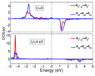
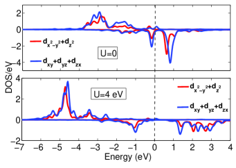
The results of the DFT calculations for the Fe dopant on the (110) surface of GaAs are shown in
Fig. 7. The lower symmetry on the surface lifts the degeneracy of the -orbitals and more peaks
appear in the DOS compared to the bulk.
The values of the TB parameters of the -orbitals of Fe on the surface are again extracted directly from
the DFT calculation with eV (see the bottom panel of Fig. 7) as the positions of the peaks in the
spin-resolved DOS for the corresponding orbitals.
In contrast to Mn, we do not tune the extracted values
for Fe on the GaAs surface. This is due to the lack of accepted experimental data on
the position of the impurity-induced states in the gap for the case of Fe on the surface.
We take the value for the spin-up on-site energy of and orbitals from the main peak of the majority DOS,
which is located at 4.5 eV. In the case of the minority DOS, we find two pronounced peaks, one above and the
other one below zero. The choice of the
positive on-site energy for the spin-down and orbitals
pushes the Fe levels into the conduction band, which seems to be an
unlikely scenario based on the bulk level-structure. Therefore
we take the value for the on-site energy for spin-down and orbitals
from the peak in the minority DOS located at -1 eV (see Table 1).
IV RESULTS AND DISCUSSION
IV.1 Mn dopants on (110) GaAs surface
We start by discussing the results of TB modeling of a single Mn dopant in GaAs.
As we will see in the following, our TB model incorporating the impurity -orbitals
reproduces the well-known features of Mn in the bulk and on the surface of GaAs,
in agreement with previous
studies. However,
we also find some interesting differences between our approach
and the classical-spin model. Strandberg et al. (2009)
These differences are mainly
related to the magnetic anisotropy of Mn on the surface and in the subsurface layers.
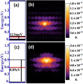
Fig. 8 shows the electronic properties of Mn in the bulk
(top panels) and on the (110) surface
(bottom panels) of GaAs. Mn introduces three levels in the GaAs gap,
with the highest level, which is unoccupied,
known as the hole-acceptor level. The other two levels are occupied and they lie below the acceptor.
The position of the acceptor level with respect to the valence band is found
at 113 meV for the bulk and at 0.89 eV for the surface dopant.
While the bulk calculation reproduces exactly the
experimental value Schairer and Schmidt (1974); Lee and Anderson (1964); Chapman and Hutchinson (1967); Linnarsson et al. (1997)
(see the discussion about the TB parametrization in section III),
the surface calculation also gives
the position of the acceptor level close to the experimental result. Kitchen et al. (2006)
As one can see from Fig. 8(c), the calculated LDOS for the acceptor on the surface
shows more concentration of the spectral weight on the Mn site compared to the bulk case, which is an
indication of a deeper and a more localized state.
In general, the calculations presented in Fig. 8 support the results
of the classical spin model Tang and Flatté (2004); Strandberg et al. (2009)
and are in good agreement with other theoretical and
experimental results. Jancu et al. (2008); Kitchen et al. (2006)
We would like to comment on one important feature of the
electronic structure of Mn in bulk GaAs.
According to Fig. 8(a)
the three levels introduced by Mn in the bulk GaAs gap
are found to be spread over an energy interval of approximately 30 meV,
when SOI is included in the calculations.
(In the Figure, the top-most level and the lowest level in the gap are split
by meV).
This is a shortcoming that the present quantum -level model shares with
the classical-spin models of
Refs. Tang and Flatté, 2004; Strandberg et al., 2009: In fact
the three (predominantly)
levels appearing in the gap should be degenerate in the perfectly
tetragonal environment of an impurity in bulk GaAs. The lifting of the
degeneracy is connected with the breaking of time reversal and rotational symmetry
in mean-field-like treatments of the kinetic-exchange coupling between
the TM impurity -levels and the levels of the nearest neighbor As atoms.
The symmetry of the Mn acceptor ground state in bulk GaAs
is an important issue. The correct framework to discuss this
problem is within a many-body approach. For a Mn in bulk GaAs,
a simplified many-body Hamiltonian that captures the salient
features of the problem consists of the Mn impurity (with ten
levels occupied on average by five electrons) and the four
nearest-neighbor As atoms. The problem is eventually reduced
to a sum of three terms: the acceptor Hamiltonian (with
single-particle degeneracy equal to six corresponding to
twice the number of levels) which in the GS is spanned by
states with five electrons (or, equivalently, one hole); the
Mn-impurity part with (on average) five electrons localized
in the orbitals of Mn2+; and a hopping Hamiltonian describing
the hybridization between As orbitals and Mn2+ orbitals.
This finite-cluster many-electron model captures the tetragonal
symmetry of the system; although (being a finite system), it is
only a rudimentary representation of the valence-band structure
at the point.
The many-body Hamiltonian can be solved
approximately by second order perturbation theory in the hopping
parameters. In the paramagnetic regime, which conserves time reversal
symmetry, the model yields a three-fold degenerate GS, corresponding
to the lowest-energy spin-multiplet , describing the effective
exchange antiferromagnetic coupling between the hole spin and
the manganese spin . The preservation of time reversal symmetry,
which can be enforced in this many-body approach, is crucial.
Note that on the general basis of group theory, irreducible representations
of in a tetragonal symmetry must necessarily be degenerate.
The case considered here is an example of this general property.
This property is lost when the Mn quantum spin is replaced by a
classical spin vector pointing in some arbitrary direction. Likewise
and for the same reason, it is also lost in any mean-field treatment
of the many-body Hamiltonian describing the Mn impurity. This is the
case of our quantum Hamiltonian, where the levels are chosen to be
spin-polarized in a similar arbitrary but fixed direction, effectively
behaving like an external magnetic field, which breaks both time and
rotational invariance. Note that this is also the case of ab-initio
spin density functional theory, whose rationale is quite close to our
d-level model. The ensuing effective one-body Hamiltonian displays
in three in-gap single-particle acceptor states of predominantly
p-character, which are typically split by an amount of the order of
the spin-orbit coupling strength. Thus the GS has degeneracy one
instead of three, as derived in the many-body approach.
It turns out that this drawback of the effective one-particle
Hamiltonian (either with the classical spin-model or with the
mean-field treatment of the levels) and its incorrect description
of the GS degeneracy is uninfluential when it comes to describing
the properties of the Mn –acceptor state which can be probed by
STM experiments, for example. The reason is that, when an electron
is added to the system (via electron tunneling, for example),
the inclusion of an interaction Hubbard U implies that only a
single state is accessible even in the many-body approach. In
other words, for typical values of the Hubbard U parameter, a
second-bound state is not found for the impurity(see, for example,
the discussion in Ref. Tang and Flatté, 2004). This important
remark justifies the use of the effective single-particle models
considered above, and explains their remarkable success in reproducing
the main features of the Mn acceptor wave functions probed in STM experiments.
A perfect three-fold degenerate level is expected for the
present model and for the models of
Ref. Tang and Flatté, 2004; Strandberg et al., 2009 when
SOI is switched off.
Indeed, our calculations show that
(i) the splitting between the three levels in the gap, as well as the
relative position of the acceptor level with respect to the top
of the valence band (113 meV) remain unchanged in very large clusters
consisting of up to
30,000 atoms,
when SOI is included.
(ii) the small splitting still present in the supercell calculations
with 3200 atoms without SOI is instead purely a finite-size effect,
which vanishes when increasing the
size of the supercell: the splitting reduces from 11.54 meV
for 3200 atoms to 0.62 meV for 20,000 atoms. That is, in the absence of SOI,
the splitting is zero for this model.
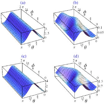
Fig. 9 shows the magnetic-anisotropy-energy landscape for a single Mn in the bulk
and on the (110) GaAs surface. The magnetic-anisotropy-energy landscape is defined as
the ground-state energy of the system plotted for different
directions of the spin quantization axis, that is, as a function of the angles and
(polar and azimuthal angles, which define the direction of the quantization axis).
The coordinate system used for these plots has parallel
to the [001] direction and (, ) parallel to [010] direction.
We compare the results obtained with our TB model (top panels) and with the
classical-spin model, introduced in Ref. Strandberg et al., 2009 (bottom panels).
The magnetic anisotropy landscape is similar for the two models. In particular, for Mn in bulk the models feature
two bistable easy axes, which are parallel to the
[001] direction and are separated by a barrier in the (001) plane
(see Figs. 9(a) and (c)).
The fact that the shape of the magnetic anisotropy
landscape does not change, means that the symmetry properties that
control this quantity are correctly represented by the classical-spin
model, or at least, they are captured in the same way as the more microscopic model.
Although the overall shapes of magnetic
anisotropy landscapes for Mn on the surface are in qualitative agreement
(see Figs. 9(b) and (d)),
the anisotropy energy is one order of magnitude smaller in
the case of our quantum -level
model. A smaller value of the anisotropy energy is consistent with the picture
of a localized acceptor level (Fig. 8).
The set of TB parameters extracted from GGA+U calculations
for Mn on the surface gives a deeper and a more localized acceptor state,
compared to the calculations done with the classical spin model Strandberg et al. (2009), which
in turn leads to lower anisotropy.

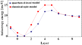
Figs. 10 and 11 show the
calculated LDOS and the anisotropy energy of the acceptor state when Mn is
successively moved down from the surface layer towards the center of the cluster.
Fig. 11 shows a comparison of the anisotropy energy calculated with the two models as
a function of the Mn depth, where we also include the values for the (110) surface and for the bulk.
Here the value of the anisotropy energy is defined to be difference between
the maximum and the minimum ground-state energy,
calculated as a function of either the direction of magnetic moment in the
case of classical-spin model, or the quantization axis in the quantum -level model.
We would like to point several important features
that can be seen on this figure. The lower value of the anisotropy energy compared to the classical-spin
model, found in our calculations, persists for almost all
of the considered subsurfaces. The relatively high anisotropy for the bulk
found in both models is a finite-size effect. In fact, our calculations demonstrate
that the bulk anisotropy energy drops to a small fraction of a meV when the number of atoms
in the cluster is increased by a factor of ten.
As Mn is moved toward the center of the cluster, one expects the anisotropy
energy to drop to its bulk value.
The present cluster (3200 atoms) includes 20 Ga layers along the [110] direction, therefore the ninth
Ga sublayer is the last sublayer where we can replace a Ga with a Mn impurity atom.
By increasing the size of the cluster we are able to place the Mn atom in the deeper sublayers.
As expected,
such calculations show that the anisotropy energy
decreases toward its bulk value as Mn is moved further away from the surface.
It is important to point out that the qualitative behavior of the magnetic
anisotropy energy landscape (for the relevant case of a Mn close to the surface)
remains unchanged with the size of the cluster. This includes the landscape of
the anisotropy energy (e.g., easy and hard axes) as well as the anisotropy energy as a
function of Mn depth (Fig. 11 of the paper). Calculations carried out
on much larger clusters Mahani et al. (2014) show that show
that the qualitative behavior of magnetic anisotropy in
Figs. 9 and 11 remains intact as a function of the cluster size, while the value of
anisotropy energy saturates to a smaller value without any qualitative change.
Note that the initial increase of the anisotropy energy up to the fifth sublayer,
and its subsequent decrease,
also reported in Ref. Strandberg et al., 2009, is most likely due to the quasi-degeneracy between
the last occupied and the acceptor states. It can be explained intuitively by looking at Fig. 10.
The acceptor wave function becomes more extended as Mn moves away from the first sublayer. Such
an extended wave function will be strongly affected by the surface until the Mn is moved
deep enough so that the surface effects start to diminish (this corresponds to the sixth sublayer).
A very small magnetic anisotropy of the first sublayer (of the order
of 0.06 meV) is due to its highly localized
wave function (see Fig. 10(a)).
The acceptor wave function in this case is less anisotropic, compared to
the surface acceptor, which can be seen from the LDOS for
easy and hard directions. The easy or hard direction here
refer to a direction of the quantization axis for which the ground state energy of the system is minimum
or maximum, respectively.
The comparison between the anisotropy energy of Mn calculated with the two models seems to indicate that
the difference is most pronounced on the surface and in the first five sublayers below the surface.
As we mentioned earlier, this is due to the fact that the surface acceptor state in
our fully quantum TB model is a deeper acceptor compared to its classical counterpart,
which leads to a lower anisotropy energy.
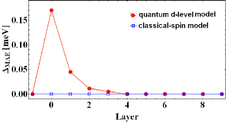
Another difference between the two models is illustrated in Fig. 12, where we plot the difference of the ground-state (GS) and the acceptor-level anisotropy energy, as a function of the Mn depth. For the classical-spin model it was found that the energy of the (single-particle) acceptor level and (many-particle) GS energy of the system are very accurately related by
| (8) |
where is a constant independent of , . This means that the sum of the two energies and is the same for any direction of the Mn magnetic moment. If and define the two directions where attains its maximum and minimum value respectively, from Eq. 8 we obtain
| (9) |
The quantity is by definition the magnetic anisotropy of the system, . Similarly, Eq. 8 implies that is the opposite of the magnetic anisotropy of the acceptor level, . Therefore, we can rewrite Eq. 9 as
| (10) |
Eq. 8 and Eq. 10 are very useful and powerful.
They imply that the total anisotropy
of the system is essentially determined by the anisotropy of the single-particle acceptor level.
This picture remains valid as long as the coupling to the conduction band is not sensitive
to the magnetization orientation.
It turns out that
in the case of
the quantum -level TB model,
Eq. 8 is not exactly satisfied.
As a result, the quantity is not exactly zero,
although, as shown in Fig. 12, its value is negligible
for most of the cases, except for the surface and the first sublayers.
We suggest that the small change in the difference of the GS and the acceptor
anisotropy energy is due to the inclusion of the -orbitals, which
brings about a magnetization-direction dependence coupling with the conduction band.
In the classical-spin model, the majority -electrons are essentially
represented by a classical vector of fixed value , which only affects
the (occupied) energy-levels of the valence band through its SOI-induced orientation dependence.
In contrast, our quantum -level model includes the impurity
-orbitals and the hopping between the -orbitals and the nearest neighbor As atoms
explicitly in the Hamiltonian. Unoccupied spin-down (minority) -levels,
located way up in the conduction
band, hybridize with like-spin As p-orbitals of the valence band.
This coupling
is responsible for the small deviation from Eq. 10,
which is also affected by the distance of the Mn atom from the surface.
as shown in Fig. 12.
IV.2 Fe dopants on (110) GaAs surface
As we showed in section IV.1, despite quantitative differences between the classical and the fully quantum treatments of the impurity magnetic moment, the classical spin model gives a good estimate of magnetic and electronic properties of the state, with a half-filled 3-shell of Mn and a bound acceptor state. However, when the electronic transitions within the -level shell of the dopant are important as in the case of Fe in GaAs, the inclusion of electrons is necessary. In this section we present the results of our fully quantum microscopic TB model for Fe in the bulk and on the (110) surface of GaAs.
Fe in the neutral acceptor state, , in GaAs has six electrons in
its shell plus a weakly bound hole. The transition from
to the neutral isoelectronic state occurs when the minority -electron
occupies the hole bound to Fe atom. A fully unoccupied minority orbitals in our TB
represents the Fe atom in its isoelectronic state (),
while the neutral acceptor state
()
is realized when one electron from the valance band occupies one of the minority -orbitals, and
creates an electron-hole excitation. (see Fig. 1).
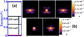
Fig. 13 shows the electronic structure and the LDOS of a single Fe
impurity in the bulk. The minority doublet () level lies at 510 meV above
the top of the valence band while the minority triplet () level is found at 370 meV above
the level. This bulk level-structure is in agreement with the results
reported previously. Malguth1 et al. (2008); Bocquel et al. (2013)
The LDOS for each of the degenerate and levels are shown in the bottom
and in the top of Fig. 13(b), respectively. The wave functions of the
two-fold generate level are highly localized
and 60% of the spectral weight is located at the Fe site. In the case of the three-fold degenerate
level almost 50% of the spectral weight is located on the Fe atom.
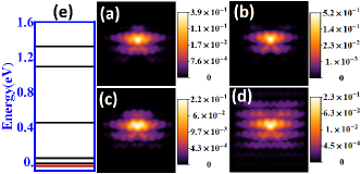
The lower symmetry of the surface compared to the bulk changes the electronic structure of the
impurity. Fig. 14(e) shows the energy level-structure inside the gap for Fe positioned
on the (110) GaAs surface. As one can clearly see from the figure,
all of the levels inside the gap, which are primarily originating from the Fe -orbitals, are split.
The two unoccupied levels immediately above the Fermi level
are closer to the valence band edge and are therefore more delocalized around
the impurity. The splitting between these two levels is 60 meV.
The LDOS calculated for this pair of states is plotted in Fig. 14(d).
The other three levels in the gap appear at 0.45 eV, 1.1 eV and 1.3 eV. The corresponding LDOS images
for each of the levels are plotted in Figs. 14(a-c). These distinct energy states
appear to be more localized on the impurity compared to the states which are closer to the valence band edge.
The shape of these acceptor states bear a striking resemblance to the STM topographies of Fe impurities on GaAs surface,
reported by Richardella et al. (see Fig. 2(c) in Ref. Richardella et al., 2009). However, we
find differences in the exact positions of the levels in the gap, compared to the
experimental data. In fact, Richardella et al. found two Fe-induced peaks
in their spectroscopic data, located at eV and eV, respectively.
We note, however, that due to the finite energy resolution of the STM, the existence of more than
one energy level within the width of a broad peak in the experimental spectroscopic data is not unlikely.
In addition, the
positions of the peaks can be modified by the tip induced band bending. One should also take into account that the splitting between the
energy levels in the gap are sensitive to the amount of the lattice distortion.
The above considerations
may provide an explanation for the quantitative differences in the in-gap level-structure obtained with our TB model and that
reported in Ref. Richardella et al., 2009. Finally, we note that in a more recent experimental study Mühlenberend et al. (2013), the authors
found evidence of six peaks in their measurements for Fe on the (110) GaAs surface. In particular, one
of the observed peaks can be related to the two closely spaced energy levels in the vicinity of the Fermi energy that
we found in our TB calculations (see Fig. 14). The occupancy of the levels close to the Fermi energy
can be different depending on the valence state of Fe, namely and .
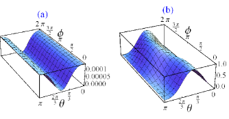
Fig. 15 shows the magnetic anisotropy energy
of the Fe impurity in the state
for different directions of the quantization axis.
The surface anisotropy
energy is approximately 1 meV, while Fe in
bulk GaAs displays a considerably smaller anisotropy energy,
of the order of meV.
The magnetic anisotropy energy landscape for the
state (not shown here) is qualitatively and
quantitatively similar to that of .
In Fig. 16
we compare the anisotropy energy for the two valence states of Fe, and ,
as the impurity atom is moved down from the (110) surface toward the
center of the cluster.
The qualitative and quantitative difference between the
anisotropy energy in the two valence states is remarkable.
While for the sublayer dependence shows strong
similarities with the case of , the
anisotropy for the the isoelectronic state is quite different: it is
typically
one order of magnitude smaller that for and depends
weakly on the sublayer.
This striking behavior can be easily understood on the basis of the discussion
leading to Eqs. 8-10.
As for the Mn impurity, the total magnetic anisotropy
of the system is closely related to the magnetic anisotropy of the acceptor levels.
As seen in Fig. 1, in the isoelectronic state
this -orbital-like acceptor level is occupied by the extra electron
that Fe has with respect to Mn.
Therefore the total energy of the system
contains also the contribution of this level. Then Eq. 10
implies that most of the
anisotropy coming from all the other occupied levels of the valance band is
essentially canceled by the approximately equal and opposite contribution coming from
the occupied acceptor. In contrast, in the valence state, the
extra electron occupies one of the higher minority -orbital levels in the gap, and the
acceptor level is empty (or is occupied by a ”hole”). Thus, as for the ,
the cancellation does not occur. Furthermore, the anisotropy of the top-most -orbital level
is, as expected, small. Therefore the behavior of is quite
similar to . These simple considerations lead us to predict
that, at least within our non-self-consistent treatment, the charged
states and should have the same behavior
of and respectively, since the
occupancy of the acceptor state is the same. This is exactly what our calculations
show. Again, we emphasize that our non-self consistent calculations should be
taken cautiously when charged states are involved.
The importance of this result stems from the fact that the valence and charge state
of individual TM impurities in GaAs can presently be manipulated with a variety of techniques.
For example, as mentioned earlier, it is possible to switch the impurity from
the to the state
via a voltage-dependent local manipulation
of the Fermi level
by means of tip-induced band bending
in STM experiments. Bocquel et al. (2013)
A similar manipulation of the Fermi level might soon allow the
switching between the and the charge state.
On the other hand, optical manipulation of the valence state might permit
switching between the and the states.
Our calculations indicate that the switching between these valence and charged
states should be also accompanied and characterized by significant changes in the
magnetic anisotropy energy of the system.
We would like to mention that for a Fe impurity in bulk, our ab-initio calculations,
in agreement with previously published results, show that the splitting
of the (minority) levels in the GaAs gap follows the behavior described
in Fig. 1. This figure shows that the dominant effect of the splitting
comes from the tetragonal symmetry of the lattice. Effects coming from
the spin-orbit interaction, which are certainly present for the ()
minority-spin level occupied by the sixth electron in Fe, seem to be small.
The situation for the Fe dopant on the surface is more complex since, as we have already
described, in this case the surface-induced broken symmetry
contributes substantially to the splitting, in a way that is not easily
disentangled from other, more intrinsic, mechanisms. In any case, it is
quite remarkable that the behavior of the anisotropy for the
complex resembles qualitatively the behavior of the : in both
cases the total anisotropy is controlled by the anisotropy of the impurity
acceptor level, regardless of whether or not an extra electron is present.
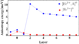
Fig. 17 shows the magnetic anisotropy landscape for the Fe impurity in the isoelectronic state as a function of its position below the surface. Although the results for the surface layer (Fig. 15(b)) and for the first sublayer (Fig. 16(a)) are similar, in the latter case the magnetic anisotropy energy is smaller. As the Fe atom is moved away from the surface, the behavior of the magnetic anisotropy approaches that found in the bulk. When Fe is placed in the ninth sublayer, i.e in the middle of the cluster, we expect it to behave like Fe in the bulk. This is confirmed in Fig. 17(i), which shows that the anisotropy energy has now decreased down to meV compared to meV for the surface and the anisotropy landscape is almost identical to its bulk counterpart (see Fig. 15(a)).
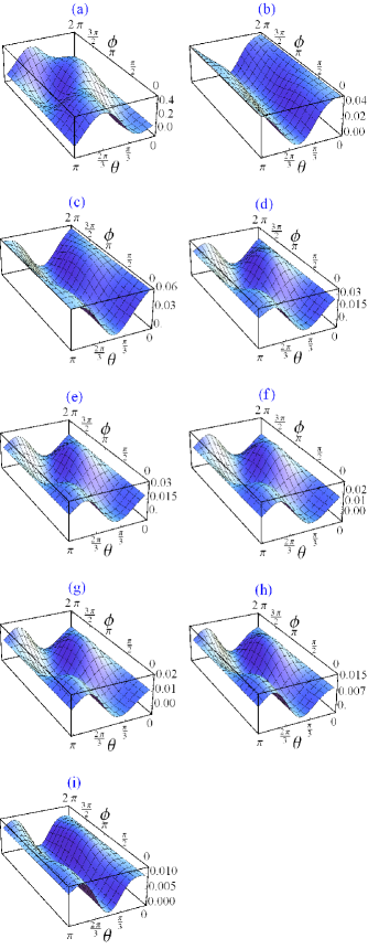
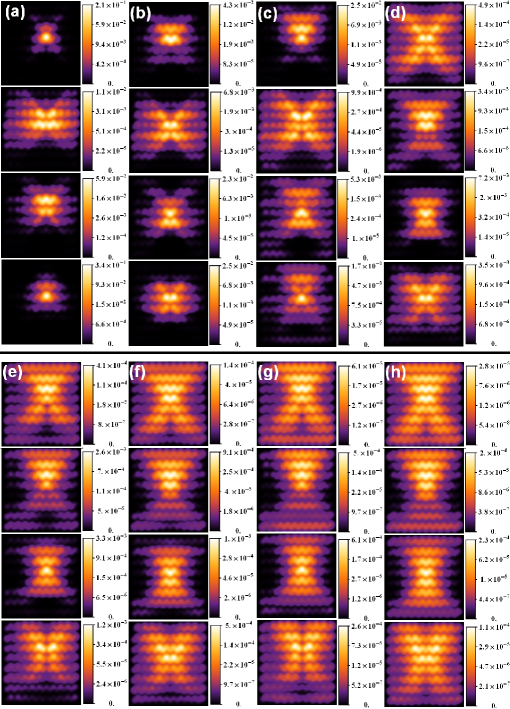
Fig. 18 shows the LDOS for the four top-most Fe-induced levels in the gap when the spin quantization axis is along the easy direction. As the Fe atom is moved down from the surface towards the center of the cluster, the concentration of the spectral weight on the impurity site decreases and the LDOS becomes more delocalized. The butterfly shape of the LDOS around the impurity is more pronounced for the sublayers located further away from the surface.
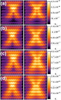
The surface LDOS for Fe in the sublayers close to the surface is not very sensitive to the direction of the spin quantization axis. However, we find that when Fe is placed between the fifth and the eighth sublayer, the calculated LDOS images do display visible differences for the easy and hard directions, as shown in Fig. 19. These changes might well be detectable by STM, when the direction of the impurity magnetic moment is changed by an external magnetic field. An estimation based on the maximum anisotropy energy of 0.05 meV (for the fifth sublayer which decreases to 0.026 meV for the eighth sublayer) for the Fe on its isoelectronic state, suggests that it should be possible to manipulate the spin of the impurity with magnetic fields of the order of T. This is very different from the case of Mn on the (110) GaAs surface. As was demonstrated in Ref. Bozkurt et al., 2013 both theoretically and experimentally, due to the strongly localized character of the Mn acceptor wavefunction on the surface and the large magnetic anisotropy energy of Mn in the near-surface layers, the acceptor hole LDOS is practically insensitive to the direction of the Mn magnetic moment in magnetic fields up to 6 T. In the case of Fe in its isoelectronic state, the combination of low anisotropy energy and the sensitivity of the surface LDOS to the direction of the impurity magnetic moment makes such manipulation possible with magnetic fields well within the experimental range.
V Conclusions
In this paper we have studied the electronic structure and
magnetic properties of individual Mn and Fe dopants in the bulk
and near the (110) surface of GaAs. Our theoretical treatment is
based on a microscopic TB model including explicitly the
-orbitals of the dopant.
We have employed DFT calculations to obtain the spin-resolved density
of states for the impurity -states, which was then used to
determine the TB parameters for the
-orbitals. We calculated the in-gap electronic level-structure, LDOS
and magnetic anisotropy landscapes for Mn and Fe impurities positioned
on the surface or in subsurface layers.
Our calculations for Mn are typically in good agreement with the results
obtained by a TB model where the impurity magnetic moment is treated
as an effective classical spin. In particular, we reproduced
the well known features of Mn in GaAs, such as the position
of the acceptor level in the gap and the spatial
character of its wavefunction both in bulk and on the surface, which are also in agreement
with experimental results.
However, the microscopic quantum model finds a lower magnetic
anisotropy energy for a Mn dopant on the surface compared to the classical-spin model.
The difference between the anisotropy energy in the two models stems from the deeper
and therefore the considerably more localized character of the acceptor state on the surface, found
in the quantum -level model.
For the case of Fe in bulk, the microscopic model correctly finds
two degenerate minority-spin levels in the gap, of predominately -character,
with the expected two-fold and three-fold degeneracy associated to the and
symmetry respectively.
The structure of these minority -character
levels changes significantly when Fe is placed on the surface or in the nearby sublayers.
Indeed, we find that the orbital degeneracy is lifted by surface effects,
and the electronic structure consists of
five unoccupied non-degenerate levels in the gap, two of which are very close to the top
of valence band, two in the middle and one close to the conduction band.
We were able to make connections between the calculated in-gap level structure
and the experimental spectroscopic data for Fe on the (110) GaAs surface.
We also presented the calculated anisotropy energy landscapes and the LDOS of the in-gap states
for Fe near the (110) surface. Importantly,
we found that the anisotropy energy of the Fe impurity on the surface and
subsurfaces depends on its valence state.
Although the neutral acceptor state behaves similarly to Mn, for
the isoelectronic state the anisotropy energy is considerably smaller,
and behaves differently as a function of the impurity depth and the orientation of its
magnetic moment. For a Fe dopant positioned in between the fifth to eighth sublayers,
the anisotropy energy drops
to a fraction of a meV.
At the same time the spatial profile of the
wavefunction associated with the top-most impurity level in the gap, is considerably
extended and therefore sensitive to the
orientation of the impurity magnetic moment.
This situation is quite different from the case of the Mn acceptor Bozkurt et al. (2013),
whose wavefunction is strongly localized for a dopant on the surface (where the anisotropy is small)
and extended for a dopant in the sublayers (where, however, the anisotropy is large).
These special
features of the Fe dopant will permit the manipulation of the Fe spin by means of an external magnetic
field of few Tesla. Under this occurrence, the results of our calculations predict that, for a Fe dopant
in its isoelectronic state,
positioned a few monolayers
below the (110) GaAs surface, a change in the direction of the dopant magnetic moment will produce
a detectable difference in the STM cross-sectional view of the LDOS of the impurity
levels in the gap.
Acknowledgments
It is a pleasure to thank A. H. MacDonald, M. E. Flatté and P. M. Koenraad for very useful discussions and collaboration. This work was supported by the Faculty of Technology at Linnaeus University, by the Swedish Research Council under Grant Number: 621-2010-3761, and the NordForsk research network 080134 “Nanospintronics: theory and simulations”. Computational resources have been provided by the Lunarc center for scientific and technical computing at Lund University.
References
- Koenraad and Flatté (2011) P. M. Koenraad and M. E. Flatté, Nat. Mater. 10, 91 (2011).
- Yakunin et al. (2004) A. M. Yakunin, A. Y. Silov, P. M. Koenraad, J. H. Wolter, W. Van Roy, J. De Boeck, J.-M. Tang, and M. E. Flatté, Phys. Rev. Lett. 92, 216806 (2004).
- Shinada et al. (2005) T. Shinada, S. Okamoto, T. Kobayashi, and I. Ohdomari, Nature (London) 437, 1128 (2005).
- Kitchen et al. (2006) D. Kitchen, A. Richardella, J.-M. Tang, M. E. Flatté, and A. Yazdani, Nature 442, 436 (2006).
- Marczinowski et al. (2007) F. Marczinowski, J. Wiebe, J.-M. Tang, M. E. Flatté, F. Meier, M. Morgenstern, and R. Wiesendanger, Phys. Rev. Lett. 99, 157202 (2007).
- Lee and Gupta (2010) D. H. Lee and J. A. Gupta, Science 330, 1807 (2010).
- Garleff et al. (2010) J. K. Garleff, A. P. Wijnheijmer, A. Y. Silov, J. van Bree, W. Van Roy, J.-M. Tang, M. E. Flatté, and P. M. Koenraad, Phys. Rev. B 82, 035303 (2010).
- Fuechsle et al. (2012) M. Fuechsle, J. A. Miwa, S. Mahapatra, H. Ryu, S. Lee, O. Warschkow, L. C. L. Hollenberg, G. Klimeck, and M. Y. Simmons, Nat. Nanotechnol. 7, 242 (2012).
- Pla et al. (2012) J. J. Pla, K. Y. Tan, J. P. Dehollain, W. H. Lim, J. Morton, D. N. Jamieson, A. S. Dzurak, and A. Morello, Nature (London) 489, 541 (2012).
- Zhao et al. (2004) Y. Zhao, P. Mahadevan, and A. Zunger, Apl. Phys. Lett. 19, 3753 (2004).
- Mahadevan et al. (2004) P. Mahadevan, A. Zunger, and D. D. Sarma, Phys. Rev. Lett. 93, 177201 (2004).
- Mikkelsen et al. (2004) A. Mikkelsen, B. Sanyal, J. Sadowski, L. Ouattara, J. Kanski, S. Mirbt, O. Eriksson, and E. Lundgren, Phys. Rev. B 70, 085411 (2004).
- Stroppa et al. (2007) A. Stroppa, X. Duan, M. Peressi, D. Furlanetto, and S. Modesti, Phys. Rev. B 75, 195335 (2007).
- Ebert and Mankovsky (2009) H. Ebert and S. Mankovsky, Phys. Rev. B 79, 045209 (2009).
- Islam and Canali (2012) M. F. Islam and C. M. Canali, Phys. Rev. B 85, 155306 (2012).
- Tang and Flatté (2004) J.-M. Tang and M. E. Flatté, Phys. Rev. Lett. 92, 047201 (2004).
- Tang and Flatté (2005) J.-M. Tang and M. E. Flatté, Phys. Rev. B 72, 161315 (2005).
- Timm and MacDonald (2005) C. Timm and A. H. MacDonald, Phys. Rev. B 71, 155206 (2005).
- Jancu et al. (2008) J.-M. Jancu, J.-C. Girard, M. O. Nestoklon, A. Lemaitre, F. Glas, Z. Z. Wang, and P. Voisin, Physical Review Letters 101, 196801 (2008).
- Strandberg et al. (2009) T. O. Strandberg, C. M. Canali, and A. H. MacDonald, Phys. Rev. B 80, 024425 (2009).
- Strandberg et al. (2010) T. O. Strandberg, C. M. Canali, and A. H. MacDonald, Phys. Rev. B 81, 054401 (2010).
- Strandberg et al. (2011) T. O. Strandberg, C. M. Canali, and A. H. MacDonald, Phys. Rev. Lett. 106, 017202 (2011).
- Mašek et al. (2010) J. Mašek, F. Máca, J. Kudrnovský, O. Makarovsky, L. Eaves, R. P. Campion, K. W. Edmonds, A. W. Rushforth, C. T. Foxon, B. L. Gallagher, V. Novák, J. Sinova, and T. Jungwirth, Phys. Rev. Lett. 105, 227202 (2010).
- Bozkurt et al. (2013) M. Bozkurt, M. R. Mahani, P. Studer, J.-M. Tang, S. R. Schofield, N. J. Curson, M. E. Flatté, A. Y. Silov, C. F. Hirjibehedin, C. M. Canali, and P. M. Koenraad, Phys. Rev. B 88, 205203 (2013).
- Garleff et al. (2008) J. K. Garleff, C. Çelebi, W. Van Roy, J.-M. Tang, M. E. Flatté, and P. M. Koenraad, Phys. Rev. B 78, 075313 (2008).
- Richardella et al. (2009) A. Richardella, D. Kitchen, and A. Yazdani, Phys. Rev. B 80, 045318 (2009).
- Bocquel et al. (2013) J. Bocquel, V. R. Kortan, C. Sahin, R. P. Campion, B. L. Gallagher, M. E. Flatté, and P. M. Koenraad, Phys. Rev. B 87, 075421 (2013).
- Mühlenberend et al. (2013) S. Mühlenberend, M. Gruyters, and R. Berndt, Phys. Rev. B 88, 115301 (2013).
- Malguth1 et al. (2008) E. Malguth1, A. Hoffmann, and M. R. Phillips, physica status solidi (b) 245, 455 (2008).
- Chadi (1977) D. J. Chadi, Phys. Rev. B 16, 790 (1977).
- Slater and Koster (1954) J. C. Slater and G. F. Koster, Phys. Rev. 94, 1498 (1954).
- Papaconstantopoulos and Mehl (2003) D. A. Papaconstantopoulos and M. J. Mehl, J. Phys.: Cond. Mat. 15, R413 (2003).
- Jancu et al. (1998) J.-M. Jancu, R. Scholz, F. Beltram, and F. Bassani, Phys. Rev. B 57, 6493 (1998).
- Chadi (1978) D. J. Chadi, Phys. Rev. Lett. 41, 1062 (1978).
- Chadi (1979) D. J. Chadi, Phys. Rev. B 19, 2074 (1979).
- Çelebi et al. (2010) C. Çelebi, J. K. Garleff, A. Y. Silov, A. M. Yakunin, P. M. Koenraad, W. Van Roy, J.-M. Tang, and M. E. Flatté, Phys. Rev. Lett. 104, 086404 (2010).
- Yakunin et al. (2007) A. M. Yakunin, A. Y. Silov, P. M. Koenraad, J.-M. Tang, M. E. Flatté, J.-L. Primus, W. V. Roy, J. D. Boeck, A. M. Monakhov, K. S. Romanov, I. E. Panaiotti, and N. S. Averkiev, Nat. Mater. 6, 512 (2007).
- Niquet et al. (2009) Y. M. Niquet, D. Rideau, C. Tavernier, H. Jaouen, and X. Blase, Phys. Rev. B 79, 245201 (2009).
- Zieliński (2012) M. Zieliński, Phys. Rev. B 86, 115424 (2012).
- Blaha et al. (2001) P. Blaha, K. Schwarz, G. K. H. Madsen, D. Kvasnicka, and J. Luitz, WIEN2k, An Augmented Plane Wave Plus Local Orbitals Program for Calculating Crystal properties (Vienna University of Technology, Austria) (2001).
- Perdew et al. (1996) J. P. Perdew, K. Burke, and M. Ernzerhof, Phys. Rev. Lett. 77, 3865 (1996).
- Soler et al. (2002) J. M. Soler, E. Artacho, J. D. Gale, A. García, J. Junquera, P. Ordejón, and D. Sánchez-Portal, Journal of Physics: Condensed Matter 14, 2745 (2002).
- Anisimov et al. (1991) V. I. Anisimov, J. Zaanen, and O. K. Andersen, Phys. Rev. B 44, 943 (1991).
- Sato et al. (2010) K. Sato, L. Bergqvist, J. Kudrnovský, P. H. Dederichs, O. Eriksson, I. Turek, B. Sanyal, G. Bouzerar, H. Katayama-Yoshida, V. A. Dinh, T. Fukushima, H. Kizaki, and R. Zeller, Rev. Mod. Phys. 82, 1633 (2010).
- Belhadji et al. (2007) B. Belhadji, L. Bergqvist, R. Zeller, P. H. Dederichs, K. Sato, and H. Katayama-Yoshida, Journal of Physics: Condensed Matter 19, 436227 (2007).
- Gopal and Spaldin (2006) P. Gopal and N. A. Spaldin, Phys. Rev. B 74, 094418 (2006).
- Schairer and Schmidt (1974) W. Schairer and M. Schmidt, Phys. Rev. B 10, 2501 (1974).
- Lee and Anderson (1964) T. Lee and W. W. Anderson, Solid State Commun. 2, 265 (1964).
- Chapman and Hutchinson (1967) R. A. Chapman and W. G. Hutchinson, Phys. Rev. Lett. 18, 443 (1967).
- Linnarsson et al. (1997) M. Linnarsson, E. Janzen, B. Monemar, M. Kleverman, and A. Thilderkvist, Phys. Rev. B 55, 6938 (1997).
- Mahani et al. (2014) M. Mahani, A. Pertsova, and C. Canali, arXiv:1402.3069 (2014).