Short-range disorder effects on electronic transport in 2D semiconductor structures
Abstract
We study theoretically the relative importance of short-range disorder in determining the low-temperature 2D mobility in GaAs-based structures with respect to Coulomb disorder which is known to be the dominant disorder in semiconductor systems. We give results for unscreened and screened short-range disorder effects on 2D mobility in quantum wells and heterostructures, comparing with the results for Coulomb disorder and finding that the asymptotic high-density mobility is always limited by short-range disorder which, in general, becomes effectively stronger with increasing ‘carrier density’ in contrast to Coulomb disorder. We also predict an intriguing re-entrant metal-insulator transition at very high carrier densities in Si-MOSFETs driven by the short-range disorder associated with surface roughness scattering.
One of the most spectacular applied physics and electronic materials advances of the last 40 years has been the 2000-fold enhancement of the low-temperature carrier mobility in molecular beam epitaxy (MBE)-grown GaAs-based 2D semiconductor structures. Between 1978, when the modulation doping technique was introduced by Störmer et al. stormer in 2D n-GaAs-AlGaAs heterostructures, and now (i.e., 2014), the electronic mobility () at low temperatures (below the Bloch-Grüneisen temperature scale, where phonons are unimportant kawamura ) has increased in 2D GaAs systems from cm2/Vs to cm2/Vs heiblum due to the steady improvement in purity, growth, fabrication, and processing techniques of individual 2D GaAs samples. As an aside, it may be pointed out that this increase in low-temperature mobility in 2D GaAs structures is comparable in magnitude to the much better known Moore’s law exponential increase in the room-temperature microprocessor speed in CMOS devices achieved over the same time scale although the qualitative origins of the two enhancements are very different (better MBE growth and improved modulation doping for individual 2D n-GaAs structures whereas better packaging and miniaturization for Si microprocessors).
In this work, we study theoretically the harmful effects of short-range disorder scattering in limiting the low-temperature electronic mobility in 2D GaAs structures, contrasting short-range disorder scattering with the corresponding long-range Coulomb disorder scattering arising from quenched charged impurities which has been extensively studied in the literature hwang1 ; hwang2 . It is well-known that Coulomb disorder arising from unintentional charged impurities in the background and from the intentional dopants needed in order to produce free carriers in semiconductors is the main mobility-limiting scattering mechanism in high-mobility 2D GaAs structures. However, at higher carrier densities, where Coulomb disorder is strongly screened out, other weaker and short-ranged scattering mechanisms arising from alloy disorder, interface roughness, neutral impurities, and defects could play a quantitative role in determining the 2D mobility in high-mobility 2D GaAs systems. Theoretically studying the quantitative effect of such short-range disorder scattering is the goal of this work.
Our theory uses the Boltzmann transport equation for calculating the carrier mobility () limited by individual scattering mechanisms by directly calculating the relevant transport relaxation or scattering time () with the mobility being defined as and the conductivity given by , where is the 2D carrier density (and the carrier effective mass). Within the leading-order Born approximation the disorder induced scattering rate is given (at ) by andormp ; dassarma2011
| (1) | |||||
Here ‘’ denotes the -th type of disorder characterized by a random distribution of scattering centers with density along the -direction nomal to the 2D layer with being the bare impurity potential and the static RPA dielectric screening function for the 2D carrier system. If screening is irrelevant as it is for most short-range disorder, we take . Also, , is the 2D carrier energy. The functions , , are to be calculated in the appropriate basis of the quasi-2D quantized confinement wavefunction (along the direction) of the 2D semiconductor structure so that they are really matrix elements in the appropriate ground subband of the 2D system. For Coulomb disorder, , where is the background lattice dielectric constant and is the impurity charge strength of the charged center producing the disorder. For short-range disorder, we assume with no loss of generality, , an uncorrelated delta-function white noise disorder characterized by a potential strength (as well as an impurity density ). It is then straightforward to calculate the short-range scattering rate
| (2) |
wgere with being the ground state quasi-2D confining wavefunction defining the quantum bound state of the 2D system along the -direction, i.e., the total single-particle ground-state wavefunction is given by , where r, k are 2D position and wave vector respectively.
If screening is neglected and the 2D system is approximated to be an idealized zero-thickness layer, then and , so that the scattering rate is a constant determined only by the strength of the short-range disorder (and carrier effective mass), becoming completely independent of 2D wave vector and carrier density. (In practice, there might be some carrier density dependence even in the absence of screening because of the quasi-2D form-factor associated with the confinement wavefunction.) If it is appropriate to screen the short-range disorder using the static RPA dielectric function , where is the 2D screening wave vector, Eq. (2) gives
| (3) |
Putting as appropriate at , Eq. (3) implies that the 2D mobility [] limited by screened short-range disorder has the following high and low-density behavior (ignoring any density dependence arising from the confinement wavefucntion effects, i.e., in the strict 2D limit)
| (4) | |||||
Thus, the high-density limit of the screened situation is the same as the unscreened case of no density dependence (since in the high-density limit), but the low-density (and strongly screened ) situation produces the somewhat counter-intuitive dependence where increasing (decreasing) 2D carrier density suppresses (enhances) the 2D mobility constrained by short-range disorder scattering. By contrast, the Coulomb disorder limited mobility behaves as with and or 3/2 depending respectively on whether the charged impurities are near or far from the 2D layer hwang2 . Thus, Coulomb disorder limited 2D mobility always increases with increasing 2D carrier density whereas the short-range disorder limited 2D mobility is either a constant independent of density or decreases with increasing density. This immediately implies that short-range disorder becomes increasingly more important at higher carrier densities where Coulomb disorder is increasingly suppressed. (In fact, similar transport behavior occurs also in graphene dassarma2011 where the low- to intermediate-density mobility is a constant because of Coulomb disorder whereas the high-density mobility decreases with increasing carrier density because of short-range scattering.) Thus, the low-temperature high-density maximum mobility of all 2D systems is eventually always limited by short-range scattering since the Coulomb disorder limited scattering is strongly and monotonically suppressed with increasing density. This behavior is well-known in 2D Si-MOSFETs andormp and in graphene hwanggraphene ; columbia , but is true for 2D GaAs systems also where the mobility must saturate (or even decrease) at high enough carrier density because any existing short-range disorder (no matter how small) arising from alloy disorder or interface roughness or neutral defects would eventually dominate the high-density mobility once the Coulomb scattering effects have become negligible. (The 2D Coulomb disorder case has recently been discussed in depth by us elsewhere hwang1 ; hwang2 .)
We note that the fact that the low (high)-density regime is more strongly (weakly) screened than the high (low)-density regime follows simply from the Fermi wave vector going as in 2D versus the screening wave vector going as a constant – the same situation applies in 3D systems too where and . This is simply a universal feature of the dimensionless quantum screening parameter increasing with decreasing carrier density in a quantum degenerate electron gas – obviously, the absolute magnitude of screening (i.e. itself) always increases with increasing density both in quantum and classical situations. While any long-range Coulomb disorder (arising from random charged impurity scattering) must always be screened, the short-range disorder may or may not always be screened depending on its physical origin – for example, the short-range disorder arising from interface roughness (atomic defects or vacancies) should typically be screened (unscreened).
We now present our detailed numerical results for 2D mobility limited by short-range scattering comparing and contrasting with the corresponding Coulomb disorder situation. Our numerical results (all at ) include full effects of the appropriate quais-2D confinement wavefunction in our calculations, both for GaAs quantum wells [where the well-width ‘’ determines ] and heterostructures [where the ground-state confinement wavefunction depends explicitly on the carrier density through the self-consistency effect stern ; andormp , thus providing an additional density dependence of the mobility]. Our use of Born approximation in the Boltzmann transport theory is justified by the high carrier density regime of our interest, and is also borne out by the extensive success of the Born approximation in calculating 2D semiconductor transport properties over the last 40 years, both for long-range Coulomb disorder and short-range interface roughness disorder. andormp We mention also that the parameters used for our transport calculations are realistic numbers for Si MOS structures andormp , but not for GaAs-based 2D systems where the interface roughness scattering is much weaker than in Si MOSFETs since the GaAs-AlGaAs interface has very little roughness with GaAs and AlGaAs being almost lattice-matched. The other differences between Si and GaAs systems are the different effective masses, background dielectric constants, and lower impurity disorder in GaAs.
In Figs. 1–3 we show respectively our numerical results for the mobility () as a function of carrier density () in GaAs-AlGaAs heterostructures (Fig. 1) and GaAs-AlGaAs quantum wells (Figs. 2 and 3). In each case, as well as the density scaling exponent of mobilityhwang2 , i.e., , are both shown for several different models of long- and short-range disorder scattering: unscreened and screened Coulomb disorder; unscreened and screened neutral short-range disorder. In Figs. 1 (heterostructure) and 2 (quantum well), the impurities are located inside the 2D electron layer whereas in Fig. 3 (quantum well) the impurities are located at the interface. The absoulte magnitude of the mobilities are not particularly relevant since the impurity densities (or the scattering strength) are not known in general, but the relative variations in the mobility as a function of density for various scattering mechanisms provide a meaningful comparison. We adjusted the various unknown impurity parameters (e.g. for Coulomb disorder and for short-ranged disorder) so that all the results for different scattering mechanisms can be fitted within the same figure. It is easy to obtain the mobility limited by arbitrary scattering strength (i.e. different values of and/or ) simply by appropriately scaling our results shown in Figs. 1–3, remembering that (or ).
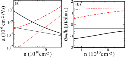
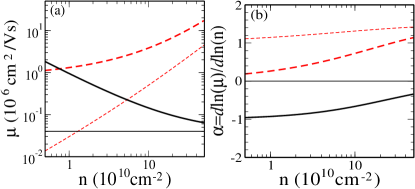
The most important qualitative results of Figs. 1–3 are the following: (i) The mobility often, but not always, could decrease with increasing density for short-range disorder scattering; (ii) the high-density mobility is always dominated by short-range disorder; (iii) a consequence of the last statement is that at sufficiently high density , where , will either become zero or become negative; (iv) the detailed quantitative aspects of short-range disorder effect on the mobility would depend on many (unknown) microscopic details such as the location of the disorder (at the interface or in the layer), screened or not, quantum well or heterostructure; (v) the 2D mobility, when limited by short-range disorder in the channel, has an exponent which is qualitatively different from the exponent limited by Coulomb disorder () – whether is actually zero or negative depends on whether the short-range disorder is screened or not; (vi) the mobility decreases linearly with , and thus it decreases linearly with the number of Al atoms (i.e. Al density) in the channel assuming that the mobility is limited by alloy disorder scattering manfra .
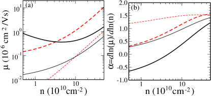
We note that it is straightforward to derive the following dependence of mobility limited by unscreened short-range disorder on the quasi-2D form-factor arising from the wavefunction confinement effect;
| (5) |
where ‘’ is the quantum well width and ‘’ is the variational parameters defining () which is given by in the simple Stern-Howard variational approximation andormp . In general, and , and thus (heterostructure) and (quantum well) for the unscreened short-range disorder. In the presence of screening, an extra factor of comes in (see Eq. 3) so that we get (heterostructure) and (quantum well) in the limit of screened short-range disorder. For , the screening effect disappears as discussed earlier.
Finally, we conclude by making an intriguing prediction about a re-entrant metal-insulator transition which should occur in 2D Si-MOSFETs at a very high carrier densities ( cm-2) driven entirely by the short-range disorder scattering associated with the surface roughness at the Si-SiO2 interface which is known to be the dominant high-density mobility-limiting mechanism andormp . As shown in Fig. 4, the Si MOSFET mobility at first increases (for ) with increasing carrier density reaching a maximum sample-dependent value at some characteristic sample-dependent density with decreasing with increasing carrier density at high densityandormp . The numerical results shown in Fig. 4 are easily understood based on the realistic model of just two scattering mechanisms, leading to mobilities limited by Coulomb impurities () and surface roughness () dominating at low () and high () densities, respectively
| (6) |
with , where , and , where . From Eq. (6), we then get
| (7) |
where and are constants (i.e. roughly independent of carrier density) which depend on the details of Coulomb disorder and surface roughness disorder, respectively. Equation (7) implies and , and thus has a maximum at a disorder-dependent non-universal density with the value . It is easy to show where and are the charged impurity disorder strength and surface roughness scattering strength, respectively. Thus, increases (decreases) with increasing charged impurity density. All of these behaviors are clearly manifest in our Fig. 4 where we show realistic numerical results for two situations with low and high values of (thus corresponding to a high- and a low-quality MOSFET sample, respectively) using the same surface roughness disorder parameters. The two sets of results in Fig. 4 [i.e., 4(a) and 4(b)] correspond to using two different sets of surface-roughness materials parameters at the Si-SiO2 interface which are in general not independently known and often inferred based on the modeling of transport measurements.
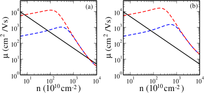
What we summarize above is known in some form in the literature on Si-MOSFET transport propertiesandormp , but now we make a striking new observation which seems to have been completely overlooked in the extensive literature on MOSFETs. We note that the transport mean free path (), , with being the Fermi velocity, is very small in Si-MOSFETs both at low carrier density (where Coulomb scattering dominates) and at high carrier density (where short-range surface roughness disorder dominates). It is well-known that Si-MOSFETs universally undergo a low-density metal-insulator transition (MIT) at a critical density (), dominated by charged impurity scattering, where the mean free path becomes short enough so that the Ioffe-Regel-Mott criterion is satisfied. This low-density MIT in Si-MOSFETs has been studied extensively in the literature over the last forty years andormp ; abrahams ; dassarma2011 . What we predict here is that the Ioffe-Regel-Mott criterion may also be satisfied at high density () where very strong short-range surface roughness scattering would eventually reduce the mobility to a low enough value ( cm2/Vs) so that would be satisfied at a second critical density () with the insulating state being re-entrant for (as well as for ) with the intermediate density regime being metallic. We show the , which is equivalent to line, in our Fig. 4 to emphasize the fact that there can, in principle, be two solutions for the integral equation at two densities, depending on the details of disorder. Our extensive numerical investigations with many possible realistic Si-MOSFET disorder parameters we find that cm-2 in general with cm-2 being the most likely value for most realistic Si-MOSFET samples. By contrast cm-2 typically depending on the amount of Coulomb disorder in the system. Of course, it is also possible that the surface roughness scattering is never strong enough to induce condition at any carrier density in which case there will be no re-entrant transition to an insulating phase at high carrier density as shown in Fig. 4(b).
If low-temperature transport measurements are feasible in Si-MOSFETs at carrier densities above cm-2, we believe that our predicted re-entrant metal-insulator transition could be observed experimentally. We emphasize, however, that the integral equation may have zero, one [Fig. 4(b)], or two [Fig. 4(a)] solutions in general depending on the details and the relative strengths of the applicable long- and short-range disorder in the system, given that for and for . The three solutions correspond respectively to the system being always localized because of very large disorder ( for all density), having an insulating phase at low density driven by Coulomb disorder and a metallic phase for all [as in Fig. 4(b)], and the re-entrant insulating case with a second insulator for [as in Fig. 4(a)] driven by strong surface roughness disorder. The first two situations are well-known in the MOSFET literature, but the re-entrant high-density insulating phase predicted here has not yet been reported experimentally to the best of our knowledge.
This work is supported by LPS-CMTC, Microsoft Q, and Basic Science Research Program through the National Research Foundation of Korea Grant funded by the Ministry of Science, ICT & Future Planning (2009-0083540).
References
- (1) H. L. Störmer, R. Dingle, A. C. Gossard, and Wiegmann, Inst. Conf. Ser. London 43, 557 (1978).
- (2) T. Kawamura and S. Das Sarma, Phys. Rev. B 45, 3612 (1992).
- (3) H. C. Choi, W. Kang, S. Das Sarma, L. N. Pfeiffer, and K. W. West, Phys. Rev. B 77, 081301(R) (2008); W. E. Chickering, J. P. Eisenstein, L. N. Pfeiffer, and K. W. West, Phys. Rev. B 87, 075302 (2013); N. Deng, A. Kumar, M. J. Manfra, L. N. Pfeiffer, K. W. West, and G. A. Csáthy, Phys. Rev. Lett. 108, 086803 (2012); W. Pan, J. S. Xia, H. L. Stormer, D. C. Tsui, C. Vicente, E. D. Adams, N. S. Sullivan, L. N. Pfeiffer, K. W. Baldwin, and K. W. West, Phys. Rev. B 77, 075307 (2008); I. P. Radu, J. B. Miller, C. M. Marcus, M. A. Kastner, L. N. Pfeiffer, K. W. West, Science 320, 899 (2008).
- (4) E. H. Hwang and S. Das Sarma, Phys. Rev. B 77, 235437 (2008).
- (5) S. Das Sarma and E. H. Hwang, Phys. Rev. B 88, 035439 (2013).
- (6) T. Ando, A. B. Fowler, and F. Stern, Rev. Mod. Phys. 54, 437 (1982).
- (7) S. Das Sarma, S. Adam, E. H. Hwang, and E. Rossi Rev. Mod. Phys. 83, 407 (2011).
- (8) E. H. Hwang, S. Adam, and S. Das Sarma, Phys. Rev. Lett. 98, 186806 (2007).
- (9) Y.-W. Tan, Y. Zhang, K. Bolotin, Y. Zhao, S. Adam, E. H. Hwang, S. Das Sarma, H. L. Störmer, and P. Kim, Phys. Rev. Lett. 99, 246803 (2007).
- (10) F. Stern and S. Das Sarma, Phys. Rev. B 30, 840 (1084); W. E. Howard and F. F. Fang, Phys. Rev. B 13, 2519 (1976).
- (11) J. D. Watson, S. Mondal, G. Gardner, G. A. Csáthy, and M. J. Manfra, Phys. Rev. B 85, 165301 (2012)
- (12) E. Abrahams, S. V. Kravchenko, and M. P. Sarachik, Rev. Mod. Phys. 73, 251 (2001).