Observation of monolayer valence band spin-orbit effect and induced quantum well states in MoX2
Abstract
Transition metal dichalcogenides have attracted much attention recently due to their potential applications in spintronics and photonics as a result of the indirect to direct band gap transition and the emergence of the spin-valley coupling phenomenon upon moving from the bulk to monolayer limit. Here, we report high-resolution angle-resolved photoemission spectroscopy on MoSe2 (molybdenum diselenide) single crystals and monolayer films of MoS2 grown on Highly Ordered Pyrolytic Graphite substrate. Our experimental results, for the first time, resolve the two distinct bands at the Brillouin zone corner of the bulk MoSe2, and provide evidence for the critically important spin-orbit split bands of the monolayer MoS2. Moreover, by depositing potassium on cleaved surfaces of these materials, the process through which quantum well states form on the surfaces of transition metal dichalcogenides is systematically imaged. We present a theoretical model to account for the observed spin-orbit splitting and the rich spectrum of the quantum well states observed in our experiments. Our findings taken together provide important insights into future applications of transition metal dichalcogenides in nanoelectronics, spintronics, and photonics devices as they critically depend on the spin-orbit physics of these materials.
In the recent years, with the discovery of two-dimensional states in graphene Novoselov2005 ; Zhang2005 ; Geim2007 and topological insulator surfaces Hasan2010 ; Qi2011 ; Hasan2011 , there has been an outburst of research activities to understand the physical properties of materials featuring two-dimensional (2D) states and their applications to optoelectronics and spintronics. One family of 2D materials that has recently attracted much attention is transition metal dichalcogenides (TMDCs) such as monolayers and few-layers of MX2 (M = Mo, W and X = S, Se) Wang2012b ; Balendhran2013 . These materials are easy to cleave, exfoliate, and fabricate Coleman2011 ; Castellanos-Gomez2012 , and have band gaps comparable in size to that of silicon (1.1 eV - 1.4 eV in bulk and 1.5 eV - 1.9 eV in monolayers) with the predicted property of transitioning from an indirect to a direct one upon reduction in size from bulk to monolayer Wang2012b ; Kobayashi1995 ; Lebegue2009 ; Ding2011 ; Kuc2011 ; Mak2010 ; Splendiani2010 , making them suitable for potential use in electronics applications such as thin film transistors. Furthermore, it has been predicted that the exotic spin-valley coupling phenomena occurs in monolayers of TMDCs, thus making them appropriate for spintronics and valleytronics devices Zhu2011 ; Xiao2012 ; Zeng2012 ; Zeng2013 . Nevertheless, even though many recent studies have examined the possibility of using transition metal dichalcogenides in single-layer transistors Radisavljevic2011 ; Yoon2011 ; Yin2012 ; Zhang2012 , and have investigated their optical properties and potential use in optoelectronics Frindt1963a ; Frindt1963b ; Kam1982 ; Zeng2012 ; Mak2010 ; Splendiani2010 , surprisingly there have only been a few experimental works on uncovering the electronic band structures of the bulk, few-layers, and monolayers of these materials and their modification under external effects such as doping, surface deposition, or heterostructuring. The few existing momentum-resolved spectroscopic studies on these materials also lack the resolution and depth to highlight the important features of their band structures Boker2001 ; Mahatha2012 ; Mahatha2012a ; Mahatha2013 ; Jin2013 . For instance, only recently using micro-ARPES the evolution of the valence band at the corner of the Brillouin zone (BZ) from higher to lower binding energies upon reducing the number of layers to monolayer has been demonstrated Jin2013 .
The interest in monolayers of the MX2 series lies in the emergence of the direct band gap as a consequence of the disappearance of van der Waals interlayer interactions in the monolayer limit Splendiani2010 ; Wang2012b , as well as the valence band strong spin-orbit splitting due to the loss of inversion symmetry Zhu2011 ; Xiao2012 ; Wang2012b ; Jin2013 . However, since films of TMDCs on typical substrates such as Si/SiO2 grow in very small flakes of 10 m 10 m and are usually composed of islands of variable thicknesses next to each other, tracking these two properties in a momentum-resolved fashion has proven to be challenging. Furthermore, the splitting of the valence band top into two distinct degenerate bands in the bulk limit due to both strong spin-orbit coupling and interlayer hopping Zahid2013 could be of interest and has not been resolved to date. Moreover, until very recently MoS2 has experimentally gotten the most attention amongst various members of the TMDCs family such as MoSe2, WS2, and WSe2. This is despite the fact that the stronger spin-orbit coupling of the later compounds make them more attractive for spintronics applications.
Thus, in this work we utilize angle-resolved photoemission spectroscopy (ARPES) to directly map the electronic band structure of bulk MoSe2 across the entire BZ. We then study the evolution of its band structure upon in-situ surface deposition with an alkali metal (potassium). Our results demonstrate the formation of a nearly free 2D electron gas (2DEG) within the potassium overlayers confined to the surface of MoSe2 in the form of quantum well states (QWSs). This quantum confinement of potassium layers could potentially enhance the optoelectronics performance of bulk and thin films of the TMDCs and be utilized in optoelectronics applications of these materials. Moreover, we resolve the band structure of a monolayer of MoS2 grown on Highly Ordered Pyrolytic Graphite (HOPG) substrate using the chemical vapor deposition (CVD) growth method and find evidence suggesting the existence of the split valence band induced by strong spin-orbit coupling and broken inversion symmetry. We compare our ARPES results with first-principles theoretical calculations to gain microscopic insights on the electron behavior in these materials which is critically important for optimizing their potential performance in device settings.
Results
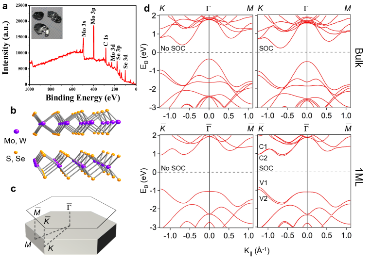
Crystal structure of MX2. The crystal structure of MX2 (M = Mo, W and X = S, Se) is a layered structure with layers of M atoms sandwiched between two layers of X atoms. These layers, which are held together through van der Waals forces, are shifted relative to each other in such a way that M atoms in one layer are placed directly above the X atoms in the neighboring layers Wang2012b ; Balendhran2013 ; Mahatha2012 . This crystal structure and the corresponding Brillouin zone are shown in Figs. 1b and 1c, respectively. The center of the BZ is the point, with points the center of the hexagonal BZ edges, and points the corners of the hexagon. , , and are the projection of these points onto the 2D surface BZ as illustrated in Fig. 1c. X-ray photoemission spectroscopy (XPS) measurements of the single crystals of MoSe2 used in our studies reveal sharp peaks corresponding to Mo 3, 3, and 3 core levels, as well as those of Se 3 and 3 as shown in Fig. 1a, thus indicating the high quality of the studied samples.
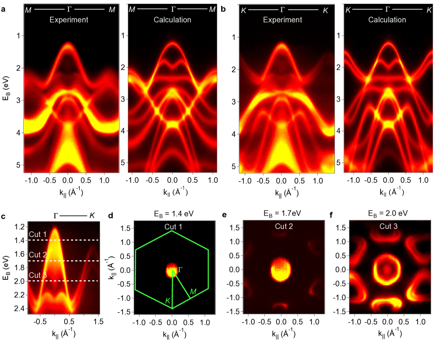
Electronic band structure of MoSe2. We start by investigating the band structure of MoSe2. The - maps of the electronic band structure measured by ARPES (left panels in Figs. 2a and 2b) along the two high symmetry directions of the BZ, and , show extraordinary resemblance to the calculated bands from the first-principles calculations (right panels in Figs. 2a and 2b). The ARPES measurements here were performed at a photon energy of = 90 eV. The kinetic energy value of the Fermi level is determined by measuring that of the polycrystalline gold separately at the same photon energies and under the same experimental conditions. The valence band maximum (VBM) is found to be located at the point of the BZ at a binding energy of 1.2 eV. The valence band just below the topmost band at binding energies of 1.7 eV - 1.9 eV, which appears clearly in our first-principles calculations has a somewhat weaker intensity in our ARPES measurements due to matrix elements effect.
One important feature of our measurements is the unambiguous observation of the two distinct bands near the top of the valence band along the direction of the BZ. These bands are highlighted in Fig. 2c, a zoomed-in version of the top part of the valence band along the direction, and are well in agreement with band structure calculations conducted here as well as the ones reported in earlier studies Wang2012b ; Lebegue2009 ; Ding2011 . Constant binding energy contours at representative binding energies of 1.4 eV, 1.7 eV, and 2.0 eV are presented in Figs. 2d - 2f. At eV, there exists only one electron-like pocket around each of the points of the BZ (see Fig. 2e), whereas two concentric pockets are observed at eV (see Fig. 2f), clearly resolving the two distinct bands at the BZ corners.
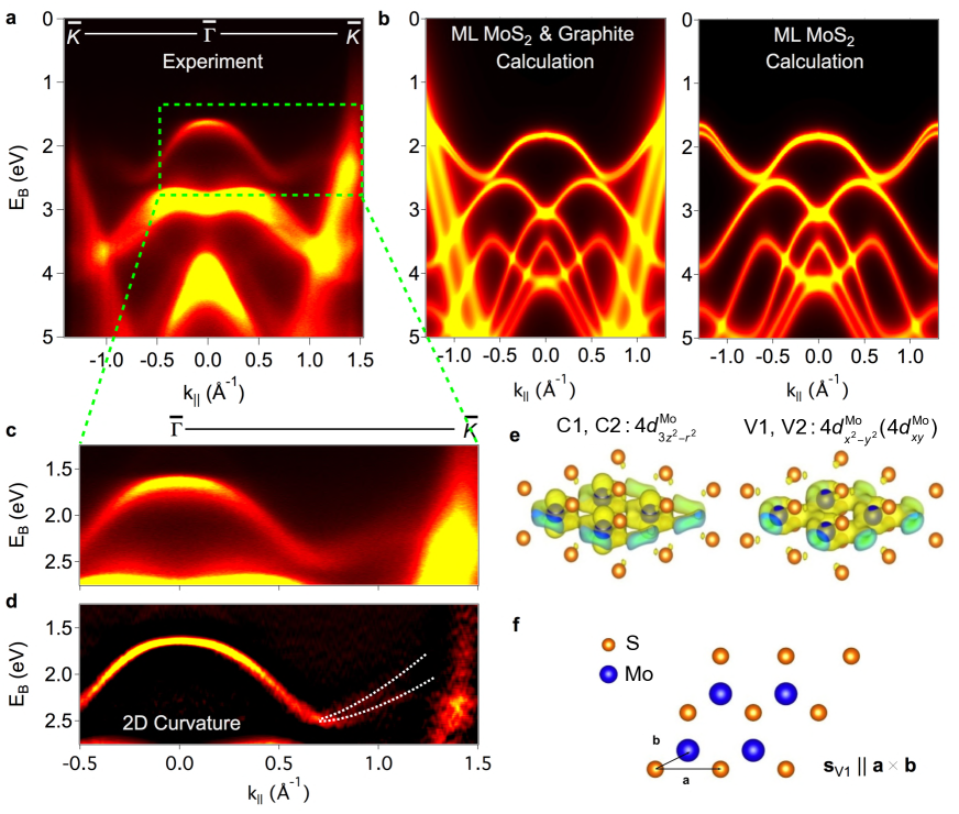
Spin-orbit induced splitting of the valence band in monolayer TMDCs. Fig. 1d shows our first-principles band structure calculations for bulk (top row) and monolayer (bottom row) MoS2, with (right column) and without (left column) considering spin-orbit coupling. These demonstrate the indirect to direct band gap transition on going to the monolayer limit and the spin-orbit splitting of the monolayer valence band in TMDCs. The Fermi level in these - maps is indicated by the dashed lines. In the next step we turn our attention to monolayer MoS2 on HOPG substrate. This conducting substrate was deliberately chosen to avoid the electronic charging of the film during the photoemission process. The - map of the electronic band structure of this sample along the high symmetry direction reveals the electronic bands of monolayer MoS2 as well as the linear bands of graphite from the HOPG substrate at the point of the BZ. We have conducted first-principles calculations of monolayer MoS2 (right panel in Fig. 3b) and the hybrid structure of this monolayer and graphite (left panel in Fig. 3b), which indicate the general agreement with our ARPES findings. Despite the existence of the graphite’s bands at the points, and their merging with the MoS2 valence band around these points of the BZ, we can still resolve a large section of the MoS2 valence band top near along the high symmetry direction , as highlighted in Fig. 3c, a zoomed-in version of Fig. 3a near the top of the valence band.
Moreover, we note the broadening of the valence band close to the Fermi level along the high symmetry direction (see Fig. 3c). Performing 2D curvature analysis Zhang2011 of the obtained bands, we resolve two split branches of the valence band of MoS2 along this high symmetry direction (close to the point) as shown in Fig. 3d. The white dotted lines are guides to the eyes for these two spin-orbit split branches of the valence band. This is consistent with the spin splitting scenario predicted to exist in this material. Monolayers of TMDCs lack inversion symmetry and are non-centrosymmetric. The in-plane confinement of electron motion and high mass of the elements in these materials result in strong spin-orbit splitting of the valence band. This property makes these materials promising candidates for applications in spintronics devices Wang2012b ; Zhu2011 ; Xiao2012 ; Zeng2013 . Our observation here is the first momentum-resolved experimental evidence for such spin-orbit splitting. Further spin-resolved ARPES studies are needed to identify the spin configuration of these split bands.
To further demonstrate the orbital property and spin texture of monolayer MoS2, we calculate the charge densities and spin expectation values of the lowest two conduction states and the topmost two valence states at marked in Fig. 1d as C1, C2, V1, and V2, respectively. The charge density plots shown in Fig. 3e indicate that the dominant orbital components are Mo and Mo for C1(C2) and V1(V2), respectively. The calculated spin expectation values of states near show nearly out-of-plane spin polarization, which can be attributed to an interplay of the pure in-plane electron motion and the inversion symmetry breaking crystal potential. The out-of-plane character of Mo explains the negligible spin splitting between the C1 and C2 states.
On the other hand, the calculated energy splitting between V1 and V2 states is 138 meV at , as a consequence of the prominent in-plane charge density variation of Mo orbital, which is in good agreement with previous results from Density Functional Theory calculations Zhu2011 . According to the calculated spin expectation values, we deploy a straightforward method to determine the spin orientation of the V1 and V2 states, which are important when considering the selection rule of polarized photon excitations. Viewing monolayer MoS2 from top, since sulfur atoms sit on the hexagonal lattices it’s alway possible to find a primitive vector connecting to adjacent sulfur atoms in the same direction as . Call this vector a and drawing another vector b from the sulfur atom at the origin of a to the nearest Mo atom, the spin orientation of V2 is in the direction of and that of V1 points to the opposite direction.
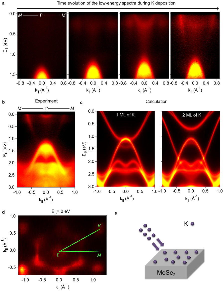
Observation of QWSs of a nearly free 2DEG by surface deposition. In order to study the effect of alkali metal deposition on the surface of bulk MoSe2, we deposit potassium (K) in-situ on cleaved surfaces of crystals of this material, and track the evolution of the band structure spectra as the deposition occurs. Deposition was performed at = 60 K with an estimated deposition rate of 0.08 - 0.09 Åmin-1. Fig. 4a shows the evolution of the band structure - map along the direction of the BZ during the deposition process. We observe that the VBM at moves closer to the Fermi level by about 200 meV. We associate this shift with the formation of a conducting layer on the surface of our sample after potassium deposition. More specifically, the VBM of the MoSe2 sample is at eV, but before deposition is shifted down by about 200 meV due to the electronic charging effect. Next, we observe the formation of new electronic states in the band gap of MoSe2, extending from the Fermi level to the valence band (see middle panels in Fig. 4a). Upon the completion of the deposition process these in-gap states are completely formed as shown in the last panel of Fig. 4a and Fig. 4b.
We note the formation of electron-like pockets on the Fermi surface after the completion of the deposition process. These pockets appear right at the points of the BZ. Since the energy spacing between these pockets and the VBM ( eV) is smaller than the indirect gap of MoSe2 ( eV) we rule out the possibility of these pockets being a part of the conduction band of MoSe2. The resulting Fermi surface after potassium deposition shows two concentric circular shaped pockets around the center of the BZ, as well as the aforementioned pockets at the points (Fig. 4d). The circular pockets around are identified as the first and second QWSs, whereas the pockets at as resulting from the surface states of potassium. We furthermore conduct first-principles calculations of potassium layers formed on the surface of bulk MoSe2 and find that our experimental observation is in qualitative agreement with two atomic monolayers of potassium deposited on the surface of MoSe2, as shown in Fig. 4c. The possibility of directly accessing the conduction band of bulk and monolayer TMDCs through intercalation and adsorption of alkali metals has been theoretically predicted Dolui2013 . Our results suggest that adsorption of alkali metals on the surface of bulk MoSe2 results in the formation of QWSs and a nearly free 2DEG rather than electron doping and providing access to the conduction band.
Discussion
The splitting of the valence band along the high symmetry direction of the monolayer MoS2 and other TMDCs which is due to strong spin-orbit coupling (because of the high mass of the elements) and lack of inversion symmetry, has been suggested in previous theoretical studies as well as our first-principles calculations here Wang2012b ; Zhu2011 . For the bulk, this splitting is caused by the combination of interlayer interaction and spin-orbit coupling. In this case, there is no spin splitting between these two bands and they are indeed spin-degenerate (Kramers’ degeneracy) due to the presence of inversion symmetry along with time reversal symmetry. But, the strong spin-orbit coupling in TMDCs results in enhanced splitting of these spin-degenerate bands at the point of the BZ (see Fig. 1d) Zahid2013 . Our results resolve these two distinct bands at the corners of the BZ through ARPES measurements and theoretical first-principles calculations. Furthermore, we have provided the first momentum-resolved experimental evidence of the spin-split valence band of monolayer MoS2 grown on HOPG substrate. However, further spin-resolved ARPES measurements are needed to confirm the spin configuration of these two split bands.
Recently, experimental evidence and theoretical prediction of valley confinement has been suggested in monolayer MoS2. Specifically, it has been suggested that the split valence band at neighboring points of the BZ ( and ) posses opposite out of plane spin configurations Xiao2012 ; Zeng2012 ; Zeng2013 . The spin-orbit splitting observed in our study of monolayers of MoS2 paves the way to more detailed studies of spin and valley physics in TMDCs. It also serves as a guide for spintronics and valleytronics applications of TMDCs.
Our results also track the evolution of the band structure of MoSe2 throughout the surface deposition process with an alkali metal (potassium). We note that short after the deposition process has started potassium atoms sit on the surface of MoSe2 in a manner that results to the partial formation of the first QWS (see second panel in Fig. 4a). Consequently, the first QWS appears in full, as shown in the third panel of Fig. 4a, and finally the first two QWSs are completely formed. In the process of surface deposition, 2D conduction channels (quantum well states) emerge on the surface of the semiconducting MoSe2 (with an indirect insulating energy gap of 1.8 eV) and, as a consequence, the electronic behavior of the system changes dramatically. This tunable feature can be utilized to quantitatively control the electronic properties of this quasi-2D material. Our investigation of the dynamical process in which a nearly free 2DEG is formed on TMDCs could have important implications for future optoelectronics studies and applications of TMDCs using surface manipulations by elements such as alkali metals on bulk, few-layers, and monolayers of these materials.
In conclusion, we have conducted detailed high-resolution ARPES and first-principles calculations studies of the electronic structure of both bulk and monolayer TMDCs. We have resolved the two distinct spin-degenerate valence bands of the bulk MoSe2, and have provided evidence for the spin-orbit split bands of the monolayer MoS2, at the corners of the BZ. We have furthermore investigated the process of the formation of QWSs on the surface of bulk MoSe2, and demonstrated the formation of a 2DEG on the cleaved surfaces of TMDCs. Our findings shed light on future applications of bulk and monolayer MoX2 in electronics and spintronics devices.
Methods
Electronic structure measurements. ARPES measurements were performed with incident photon energies of 35 - 100 eV at beamline 4.0.3 of the Advanced Light Source (ALS) in the Lawrence Berkeley National Laboratory (LBNL). Samples were cleaved in-situ between 10 and 20 K at chamber pressure better than torr resulting in shiny surfaces. Energy resolution was better than 15 meV and momentum resolution was better than 1% of the surface BZ.
Sample growth. To prepare MoS2 films, molybdenum chloride (MoCl5) and sulfur powder were used as precursors and the growth of monolayer films was carried out in a CVD chamber. The ultrasonicated cleaned HOPG substrates were loaded into the CVD chamber 6 cm away from the central hot zone. Argon (Ar) gas was used as carrier gas in a pressure of 3 torr. Single crystals of MoSe2 were grown by the chemical vapor transport method, using I2 as the transporting agent. They were formed in silver-colored, graphite-like, single crystalline platelets up to 10 10 mm2 in surface area and 2 mm in thickness (inset in Fig. 1a).
First-principles calculation methods. First-principles calculations of the electronic structures were performed using HGH-type pseudo-potentials Hartwigsen1998 and a plane-wave basis set. The main program employed was developed by the ABINIT group Gonze2002 ; Gonze2005 . Spin-orbit coupling was included, where appropriate, using the relativistic LDA approximation. The experimental resolution was taken into account in the spectral simulations of Figs. 2, 3, and 4, but the matrix elements effect was not considered.
References
- (1) Novoselov, K. S. et al. Two-dimensional atomic crystals. Proc. Natl. Acad. Sci. U.S.A. , 10451-10453 (2005).
- (2) Zhang, Y., Tan, Y-W., Stormer, H. L. & Kim, P. Experimental observation of the quantum Hall effect and Berry’s phase in graphene. Nature , 201-204 (2005).
- (3) Geim, A. K. & Novoselov, K. S. The rise of graphene. Nat. Mater. , 183-191 (2007).
- (4) Hasan, M. Z. & Kane, C. L. Topological Insulators. Rev. Mod. Phys. , 3045 (2010).
- (5) Qi, X-L. & Zhang, S-C. Topological insulators and superconductors. Rev. Mod. Phys. , 1057 (2011).
- (6) Hasan, M. Z. & Moore, J. E. Three dimensional topological insulators. Rev. Mod. Phys. , 3045 (2010).
- (7) Wang, Q. H., Kalantar-Zadeh, K., Kis, A., Coleman, J. N. & Strano, M. S. Electronics and optoelectronics of two-dimensional transition metal dichalcogenides. Nat. Nanotechnol. , 699-712 (2012).
- (8) Balendhran, S. et al. Two-dimensional molybdenum trioxide and dichalcogenides. Adv. Funct. Mater. , 3952-3970 (2013).
- (9) Coleman, J. N. et al. Two-dimensional nanosheets produced by liquid exfoliation of layered materials. Science , 568-571 (2011).
- (10) Castellanos-Gomez, A., Barkelid, M., Goossens, A. M., Calado, V. E., van der Zant, H. S. J. & Steele, G. A. Laser-thinning of MoS2: on demand generation of a single-layer semiconductor. Nano Lett. , 3187-3192 (2012).
- (11) Kobayashi, K. & Yamauchi., J. Electronic structure and scanning-tunneling-microscopy image of molybdenum dichalcogenide surfaces. Phys. Rev. B , 17085-17095 (1995).
- (12) Lebègue, S. & Eriksson. O. Electronic structure of two-dimensional crystals from ab initio theory. Phys. Rev. B , 115409 (2009).
- (13) Ding, Y., Wang, Y., Ni, J., Shi, L., Shi, S. & Tang, W. First principles study of structural, vibrational and electronic properties of graphene-like MM2 (M=Mo, Nb, W, Ta; X=S, Se, Te) monolayers. Physica B: Cond. Matt. , 2254-2260 (2011).
- (14) Kuc, A., Zibouche, N. & Heine. T. Influence of quantum confinement on the electronic structure of the transition metal sulfide S2. Phys. Rev. B , 245213 (2011).
- (15) Mak, K. F., Lee, C., Hone, J., Shan, J. & Heinz, T. F. Atomically thin MoS2: a new direct-gap semiconductor. Phys. Rev. Lett. , 136805 (2010).
- (16) Splendiani, A. et al. Emerging photoluminescence in monolayer MoS2. Nano Lett. , 1271-1275 (2010).
- (17) Zhu, Z. Y., Cheng, Y. C. & Schwingenschlögl, U. Giant spin-orbit-induced spin splitting in two-dimensional transition-metal dichalcogenide semiconductors. Phys. Rev. B , 153402 (2011).
- (18) Xiao, D., Liu, G-B., Feng, W., Xu, X. & Yao, W. Coupled spin and valley physics in monolayers of MoS2 and other group-VI dichalcogenides. Phys. Rev. Lett. , 196802 (2012).
- (19) Zeng, H., Dai, J., Yao, W., Xiao, D. & Cui, X. Valley polarization in MoS2 monolayers by optical pumping. Nat. Nanotechnol. , 490-493 (2012).
- (20) Zeng, H. et al. Optical signature of symmetry variations and spin-valley coupling in atomically thin tungsten dichalcogenides. Sci. Rep. , 1608 (2013).
- (21) Radisavljevic, B., Radenovic, A., Brivio, J., Giacometti, V. & Kis. A. Single-layer MoS2 transistors. Nat. Nanotechnol. , 147-150 (2011).
- (22) Yoon, Y., Ganapathi, K. & Salahuddin, S. How good can monolayer MoS2 transistors be? Nano Lett. , 3768-3773 (2011).
- (23) Yin, Z. et al. Single-layer MoS2 phototransistors. ACS Nano , 74-80 (2012).
- (24) Zhang, Y., Ye, J., Matsuhashi, Y. & Iwasa, Y. Ambipolar MoS2 thin flake transistors. Nano Lett. , 1136-1140 (2012).
- (25) Frindt, R. F. The optical properties of single crystals of WSe2 and MoTe2. J. Phys. Chem. Solids , 1107-1108 (1963).
- (26) Frindt, R. F. & Yoffe, A. D. Physical properties of layer structures: optical properties and photoconductivity of thin crystals of molybdenum disulphide. Proc. R. Soc. London, Ser. A , 69-83 (1963).
- (27) Kam, K. K. & Parkinson, B. A. Detailed photocurrent spectroscopy of the semiconducting group VIB transition metal dichalcogenides. J. Phys. Chem. A , 463-467 (1982).
- (28) Böker, Th. et al. Band structure of MoS2, MoSe2 and -MoTe2: angle-resolved photoelectron spectroscopy and ab initio calculations. Phys. Rev. B , 235305 (2001).
- (29) Mahatha, S. K., Patel, K. D. & Menon. K. S. R. Electronic structure investigation of MoS2 and MoSe2 using angle-resolved photoemission spectroscopy and ab initio band structure studies. J. Phys.: Condens. Matter , 475504 (2012).
- (30) Mahatha, S. K. & Menon. K. S. R. Inhomogeneous band bending on MoS2(0001) arising from surface steps and dislocations. J. Phys.: Condens. Matter , 305502 (2012).
- (31) Mahatha, S. K. & Menon. K. S. R. Quantum well states in Ag thin films on MoS2(0001) surfaces. J. Phys.: Condens. Matter , 115501 (2013).
- (32) Jin, W. et al. Direct measurement of the thickness-dependent electronic band structure of MoS2 using angle-resolved photoemission spectroscopy. Phys. Rev. Lett. , 106801 (2013).
- (33) Zahid, F., Liu, L., Zhu, Y., Wang, J. & Guo, H. A generic tight-binding model for monolayer, bilayer and bulk MoS2. AIP Adv. , 052111 (2013).
- (34) Zhang, P., Richard, P., Qian, T., Xu, Y-M., Dai, X. & Ding. H. A precise method for visualizing dispersive features in image plots. Rev. Sci. Instrum. , 043712-043712 (2011).
- (35) Dolui, K., Rungger, I., Das Pemmaraju, C. & Sanvito, S. Possible doping strategies for MoS2 monolayers: an ab initio study. Phys. Rev. B , 075420 (2013).
- (36) Hartwigsen, C., Goedecker, S. & Hutter, J. Relativistic separable dual-space Gaussian pseudopotentials from H to Rn. Phys. Rev. B , 3641-3662 (1998).
- (37) Gonze, X. et al. First-principles computation of material properties: the ABINIT software project. Comput. Mater. Sci. , 478-492 (2002).
- (38) Gonze, X., Rignanese, G-M. & Caracas, R. First-principle studies of the lattice dynamics of crystals, and related properties. Z. Kristallogr. , 458-472 (2005).