Charge density waves as the origin of dip-hump structures in differential tunneling conductance of cuprates: the case of -wave superconductivity
Abstract
Conductance-voltage characteristics (CVCs) for non-symmetric tunnel junctions between -wave superconductors with charge-density waves (CDWs) and normal metals were calculated. It was shown that they have a V-like form at small voltages and are asymmetric at larger owing to the presence of CDW peak in one of the -branches. The spatial scatter of the dielectric (CDW) order parameter smears the CDW peak into a hump and induces a peak-dip-hump structure (PDHS) typical of CVCs observed for such junctions. At temperatures larger than the superconducting critical temperature, the PDHS evolves into a pseudogap depression. The results agree well with the scanning tunneling microscopy data for Bi2Sr2CaCu2O8+δ and YBa2Cu3O7-δ.
pacs:
71.45.Lr, 74.55.+v, 74.81.-gHigh- superconductors demonstrate a number of features which are widely discussed but badly understood. Among the most enigmatic of them is the pseudogap (PG) coexisting with superconductivity at various low and intermediate dopings.gabovich10:681070 ; ekino11:699 ; sacuto13:022502 In particular, the differential current-voltage characteristics (CVCs) , where is the quasiparticle current and the bias voltage, of tunnel junctions involving high- oxides reveal a depletion at temperatures, , above and below the critical temperature, . Another CVC peculiarity is a robust peak-dip-hump structure (PDHS) observed at low temperatures ,fischer07:353 ; ekino07:180503 ; mourachkine07:956 ; zasadzinski08:833 ; krasnov09:214510 ; suzuki12:010112 ; berthod13:014528 with the CVCs in the case of superconductor (S)–insulator (I)–normal metal (N) junction often demonstrating bias-voltage asymmetry. The PDHS is also found in the angle-resolved photoemission (ARPES) spectra for a good many oxides.kordyuk02:077003 ; borisenko03:207001 ; wei08:097005 The existing explanations of PDHS are mostly based on the assumption of extremely strong coupling between electrons and either spin fluctuationschubukov98:4716 ; eschrig00:3261 or phonons.kulic05:092505 ; citro06:014527 However, in this case the PG should be attributed to some other physical reasons, which seems quite unnatural in view of the conclusions drawn from tunneling spectroscopic data.bae08:094519 ; vedeneev10:054501 Anyway, the PG and the PDHS are considered as unrelated phenomena.
We propose a different model, which enables all those peculiarities to be described from the same position. It is based on two pieces of evidence that can be regarded reliably established for high- oxides: (i) plenty of cuprates reveal, directly or indirectly, charge density waves (CDWs) competing with the Cooper pairing-induced reconstruction of the electron spectrum,gabovich10:681070 ; ekino11:699 ; gabovich13:301 and (ii) high- superconductors are inherently non-uniform objects.boyer07:802 ; pasupathy08:196 ; alldredge13:104520 The former is most probably a consequence of the reduced system dimensionality and the resulting Fermi surface (FS) nesting, whereas the latter may be an intrinsic feature associated with the oxygen non-stoichiometry.
A characteristic feature of CVCs in the case of non-symmetric S–I–N junctions is their non-symmetric behavior.renner98:149 ; fischer07:353 ; zasadzinski08:833 ; berthod13:014528 For instance, the PDHS below is the most pronounced at a negative bias voltage polarity, which corresponds to electron ejection, and the pseudogap depletion above is also non-symmetric with respect to the bias polarity. Moreover, the PDHSs are sometimes observed in both branches, the ratio between their magnitudes being different. Such a non-symmetricity can be easily interpreted in the framework of our theory by making allowance for the CDW phase (see below). Nevertheless, the adopted phenomenological approach makes the appearance of PDHS in either of the branches equiprobable. Therefore, an additional microscopic consideration should be invoked for the explanation of CVC non-symmetricity.
We should mention three additional scenarios ensuring the CVC asymmetry. One of them involves a substantial role of the Van Hove singularity in the density of states.levydecastro08:267004 ; levydecastro10:099702 ; berthod13:014528 The acceptance of this viewpoint leads to certain problems,onufrieva10:099701 ; carbotte11:066501 the discussion of which goes beyond the scope of this article. The second one suggests the decisive role of the superconducting-gap energy dependence , so that the slope is responsible for the asymmetry.hirsch99:11962 Here, is the Fermi energy. However, in this case neither of the two humps is suppressed, which contradicts the observations. The third scenario introduces strong many-body correlations making electron- and hole-like excitations nonequivalent.anderson06:1 The importance of the factor concerned cannot be ruled out, in principle, although the absence of the gap-driven peak asymmetry in other strongly correlated superconductors does not count in favor of this viewpoint.
In this article, we restrict the consideration to tunnel spectra measured for non-symmetric S-I-N junctions with the quasiparticle current flowing along the crystal -axis, i.e. perpendicularly to CuO2 layers, which as appropriate to the scanning tunneling microscopy (STM) setup. Moreover, we consider only the case of -wave symmetry of the superconducting order parameter predominately adopted by the community,tsuei08:869 although its true symmetry is still not known.klemm05:801 ; zhao11:038302
Our model of the partially gapped CDW -wave superconductor (CDWS) with the two-dimensional electron spectrumgabovich10:681070 ; ekino11:699 ; gabovich13:104503 ; gabovich13:301 was developed on the basis of its predecessor developed for the partially gapped (dielectrized) -wave superconductor.bilbro76:1887 ; gabovich03:2745 It was applied to cuprates with the checkerboard (biaxial, the number of the CDW sectors ) or unidirectional () CDW patterns. Here, for brevity, we present only the results obtained for . The second electrode is chosen to be a normal metal with a constant electron density of states; e.g., a tip of the STM device.
The -wave CDWS spectrum is a result of interaction between two pairing mechanisms, the non-isotropic net electron-electron attraction and the isotropic electron-hole (excitonic or Peierls) one. When the Cooper pairing is “switched off”, only a parent CDW phase with the complex zero-temperature dielectric order parameter and the critical temperature of partial dielectrization exists. Here, is the Euler constant, and the Boltzmann constant . At , the magnitude of dielectric order parameter varies as
| (1) |
where is the standard (-wave) Mühlschlegel dependence with (Ref. muhlschlegel59:313, , see Fig. 1). The function is assumed to be constant (the -wave symmetry) within each of four FS d-sectors. These sectors are oriented crosswise in pairs along the lattice and axes in the momentum space, with each of the sectors having the angular width . Introducing the angular factor equal 1 within each sector and 0 outside, where is the angle in the two-dimensional plane in the momentum space reckoned, e.g., from the direction, the profile of the parent dielectric order parameter over the FS can be presented in the factorized form
| (2) |
At the same time, if the CDW pairing is “switched off”, we obtain a parent -wave BCS superconductorwon94:1397 with the lobes of the superconducting order parameter also oriented in the and directions, i.e. in the same (antinodal) directions as the bisectrices of CDW sectors (the -wave symmetry). In contrast to the parent order parameter, the -space profile of its -counterpart is extended over the whole FS. It can also be presented in the factorized form
| (3) |
with the angular factor . At , where is the base of natural logarithms,
| (4) |
where is the superconducting order parameter dependence in the case of -wave pairing.won94:1397
(a)
 (b)
(b)
While describing the interplay between both pairings, we assume the angular functions to remain intact. This mutually detrimental interplay leads to the drastic difference of the actual and functions from the parent ones— and , respectively—in the interval of their coexistence [see Fig. 1(a)]. The corresponding profile [cf. Eq. (3)]
| (5) |
emerges on the non-dielectrized (nd) FS sections, and the gap
| (6) |
where
| (7) |
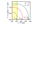
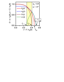
on the dielectrized (d) ones. The relevant self-consistent set of equations, which is to be solved to determine and for the given set of problems parameters , can be found elsewhere.gabovich09:224501 ; gabovich10:681070 ; ekino11:699 ; ekino11:385701 Now, neither of the order parameters can be described by the function or . Besides, one of the parent critical temperatures, or —to be more accurate, the minimum one—changes to or , respectively. Moreover, at some -combinations, the phenomenon of -reentrance emerges consisting in that within a certain temperature interval [Fig. 1(b)].
The quasiparticle current flowing through an CDWS-I-N junction along the crystal -axis includes three components,
| (8) |
Here,
| (9) |
| (10) |
| (11) |
the factor
| (12) |
is associated with the density of states in the gapped CDWS, the kernel
| (13) |
makes allowance for the Fermi statistics of charge distribution over the energy levels, is the elementary charge, and is the normal-state resistance of the junction. Any issues related to the tunneling directionality are left beyond the scope of consideration, since they lead only to minor quantitative corrections. Term (11) is generated by Green’s function describing the electron-hole dielectric pairing.gabovich10:681070 ; ekino11:699 ; gabovich13:301 The CDW phase entering the expression for the Green’s function is usually pinned by the junction interface and acquires the values 0 or . This circumstance is responsible for the CVC asymmetrygabovich97:7785 (see also the earlier work, Ref. artemenko84:691, ) needed to reproduce ’s observed for non-symmetric junctions with high- superconductors.fischer07:353 ; zasadzinski08:833 ; jenkins09:227001
The further consideration is convenient to be carried out using the normalized quantities , , , and . The dimensionless conductance was found by reproducing the actual procedure of experimental determination (see discussion in Ref. ekino08:425218, ); namely, we numerically calculated the ratio
| (14) |
An additional argument for this choice is the fact that the same procedure remains adequate when calculating the averaged (see below). The bias-voltage increment was found to insignificantly modify the result obtained if it is selected from the interval . Smaller -values gave rise to a “noise” associated with the finite accuracy of numerical calculations, and larger ones to the redundant smoothing of CVC peculiarities, especially noticeable at low temperatures. In specific calculations, we used the value .
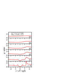
In this article, we do not carry out a full analysis of the tunnel CVCs with respect to the choice of problem parameters. Therefore, in Fig. 2, we present only the results of calculations representing the influence of on the CVC shape for two characteristic CDWS cases, without [panel (a)] and with [panel (b)] the -reentrance. The panels demonstrate how effectively CDWs distort the CVC symmetricity. It is especially clearly seen from panel (b), where the dimensionless reentrance temperature , and the CVCs remain symmetric below this temperature, because the CDWs are totally suppressed at [see Fig. 1(b)]. In both cases, the structure of PG depletion above the critical temperature [ in panel (a) and 0.41 in panel (b)] is reproduced excellently. But at low ’s, the CDW-induced peaks [Fig. 2(a)] are much stronger than the smeared humps inherent to junctions with Bi2Sr2CaCu2O8+δ or YBa2Cu3O7-δ. Nevertheless, in several intrinsic tunneling structures such huge pseudogap peaks comparable to coexisting superconductivity-related coherence peaks were also observed,krasnov00:5860 ; krasnov02:140504 ; yurgens03:147005 ; suzuki12:214529 which might be caused by specific properties of those very junctions (a high degree of uniformity, which agrees well with our conjectures). Earlier data on the YBa2Cu3O7-δ/Pb (in the normal state) junctiongurvitch89:1008 also showed the coherence peak and the hump of comparable heights.
(a)
 (b)
(b)
Making allowance for the spatial non-uniformity of CDWS resolves this discrepancy easily. In the simplest instance analyzed here, we assumed that the non-uniformity reveals itself in the spread of parameter . The calculations were carried out, similarly to Ref. gabovich07:064516, , using formula (14), where the current was additionally averaged over the interval ,
| (15) |
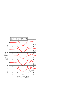
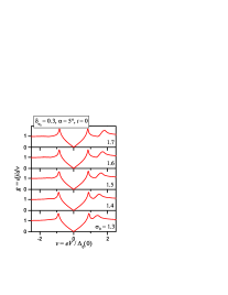
with the bell-shaped weight function . Figure 3 demonstrates the effectiveness of this procedure that drastically smears the large CDW peak, reduces its amplitude, and generates a PDHS typical of the CVCs for CDWS-I-N junctions at low ’s.

In Fig. 4, a combined action of the -spread and the temperature is illustrated. The lowest two plots describe the formation of PDHS. The other plots illustrate how all gross features in the observed CVC transform into one another as grows. Specifically, at , a noticeable asymmetric PDHS is observed with the coherence peak higher than the hump in the positive-bias branch. The negative-bias branch contains a coherence superconducting peak and the remnants of the almost compensated and strongly smeared CDW one. For , the branches would interchange.gabovich07:064516 According to the accepted model it means that CDWs are pinned with . As was said above, such a preference cannot be explained in the framework of the phenomenological approach. In the framework of our model, we can only guess that the applied electric field rearranges the CDW superstructure near the CDWS-I interface to minimize the total system energy. In this connection, it is important to bear in mind that the CDW patterns at the high- oxide crystal surface are different from their bulk counterparts, so that they may become vulnerable under the influence of the applied Coulomb field.rosen13:1977
Heating smears all gap-driven features, so that only a typical shallow pseudogap depression remains, which is in agreement with the -axis intrinsic tunneling spectroscopy data for Bi2Sr2CaCu2O8+δ.krasnov09:214510 ; suzuki12:010112 The depression extends to relatively large because the correction to Ohm’s law is proportional to
| (16) |
due to the contribution from Green’s function responsible for electron-hole pairing.gabovich95:7437
It is worth emphasizing the following circumstance. As follows from Figs. 3 and 5, by varying the parameters , , and , we can substantially modify the height of the smeared CDW hump and the distance between the hump and the coherent peak in the PDHS. But the structures observed in real experiments are reproduced the best when the parameter falls within the interval 3–10∘. Estimations on the basis of experimental data bring about a value of 15∘.gabovich13:104503 However, one should note that our model contains certain simplifications. In particular, it assumes that is constant, being the same on both pairs of nested FS sections and vanishing in a jump-like manner at their boundaries; i.e. the influence of CDWs on superconductivity is as strong as possible in the framework of the assumptions made. More realistic corrections to those rather strict conditions will inevitably enlarge the selected phenomenological value of and make it closer to the experimental one. It is necessary to bear in mind that the Cooper pairing strength is inhomogeneous as well (since both involved order parameters are interrelatedgabovich09:224501 ; gabovich10:681070 ; ekino11:699 ; ekino11:385701 ), but to a much lesser extent.boyer07:802 That is why we considered as a fixed normalizing parameter.
(a)
 (b)
(b)
In order to find out the doping dependence of the tunnel spectra in the framework of our model, it would have been necessary to change both control parameters , and simultaneously using the correlated experimental data for certain cuprate families. However, to estimate the main trend it is enough to change the parameter alone. Then one can see that the coherence-peak-to-hump energy distance increases nonlinearly with , which is quite natural and corresponds to the transition from the optimal-doping to underdoping compositions with larger PGs. It is in accordance with the experiment, e.g., with tunnel data for Bi2Sr2Ca2Cu3O10+δ.berthod13:014528 We emphasize that the original analysis of the same data based on the peak-to-dip energy dependence seems to be misleading because the dip itself is an artifact as a trough between two ridges, each having a certain physical meaning.
To summarize, we have shown that CDWs can be considered as the driving force of the pseudogap gapping revealed in tunneling spectra of -wave superconductors. The spatial inhomogeneity transforms a smeared PG into a hump which constitutes one shoulder of the PDHS observed below . The coherence peak of the superconducting origin forms another shoulder. The resulting PDHS is observed only in one branch of the current-voltage characteristics due to the loss of symmetry caused by the actual realization of a certain CDW phase ( or ). Undoubtedly, the proposed theory describing the role of CDWs in the formation of such ubiquitous features in the CVCs of tunnel junctions involving high- oxides as the pseudogap and the dip-hump structure is also applicable to the case of symmetric junction and will be considered elsewhere.
The work was partially supported by the Project N 8 of the 2012-2014 Scientific Cooperation Agreement between Poland and Ukraine.
References
- (1) A. M. Gabovich, A. I. Voitenko, T. Ekino, M. S. Li, H. Szymczak, and M. Pȩkała, Adv. Condens. Matter Phys. 2010, Article ID 681070 (2010).
- (2) T. Ekino, A. M. Gabovich, M. S. Li, M. Pȩkała, H. Szymczak, and A. I. Voitenko, Symmetry 3, 699 (2011).
- (3) A. Sacuto, Y. Gallais, M. Cazayous, M-A. Méasson, G. D. Gu, and D. Colson, Rep. Prog. Phys. 76, 022502 (2013).
- (4) Ø. Fischer, M. Kugler, I. Maggio-Aprile, and C. Berthod, Rev. Mod. Phys. 79, 353 (2007).
- (5) T. Ekino, A. M. Gabovich, M. S. Li, M. Pȩkała, H. Szymczak, and A. I. Voitenko, Phys. Rev. B 76, 180503 (2007).
- (6) A. Mourachkine, Physica C 460-462, 956 (2007).
- (7) J. F. Zasadzinski, in Superconductivity. Vol. 2: Novel Superconductors, edited by K. H. Bennemann and J. B. Ketterson (Springer, Berlin, 2008), p. 833.
- (8) V. M. Krasnov, Phys. Rev. B 79, 214510 (2009).
- (9) M. Suzuki, R. Takemura, K. Hamada, M. Ohmaki, and T. Watanabe, Jpn. J. Appl. Phys. 51, 010112 (2012).
- (10) C. Berthod, Y. Fasano, I. Maggio-Aprile, A. Piriou, E. Giannini, G. Levy de Castro, and Ø. Fischer, Phys. Rev. B 88, 014528 (2013).
- (11) A. A. Kordyuk, S. V. Borisenko, T. K. Kim, K. A. Nenkov, M. Knupfer, J. Fink, M. S. Golden, H. Berger, and R. Follath, Phys. Rev. Lett. 89, 077003 (2002).
- (12) S. V. Borisenko, A. A. Kordyuk, T. K. Kim, A. Koitzsch, M. Knupfer, J. Fink, M. S. Golden, M. Eschrig, H. Berger, and R. Follath, Phys. Rev. Lett. 90, 207001 (2003).
- (13) J. Wei, Y. Zhang, H. W. Ou, B. P. Xie, D. W. Shen, J. F. Zhao, L. X. Yang, M. Arita, K. Shimada, H. Namatame, M. Taniguchi, Y. Yoshida, H. Eisaki, and D. L. Feng, Phys. Rev. Lett. 101, 097005 (2008).
- (14) A. V. Chubukov and D. K. Morr, Phys. Rev. Lett. 81, 4716 (1998).
- (15) M. Eschrig and M. R. Norman, Phys. Rev. Lett. 85, 3261 (2000).
- (16) M. L. Kulić and O. V. Dolgov, Phys. Rev. B 71, 092505 (2005).
- (17) R. Citro, S. Cojocaru, and M. Marinaro, Phys. Rev. B 73, 014527 (2006).
- (18) M-H. Bae, J-H. Park, J-H. Choi, H-J. Lee, and K-S. Park, Phys. Rev. B 77, 094519 (2008).
- (19) S. I. Vedeneev, B. A. Piot, and D. K. Maude, Phys. Rev. B 81, 054501 (2010).
- (20) A. M. Gabovich and A. I. Voitenko, Fiz. Nizk. Temp. 39, 301 (2013).
- (21) M. C. Boyer, W. D. Wise, K. Chatterjee, M. Yi, T. Kondo, T. Takeuchi, H. Ikuta, and E. W. Hudson, Nature Phys. 3, 802 (2007).
- (22) A. N. Pasupathy, A. Pushp, K. K. Gomes, C. V. Parker, J. Wen, Z. Xu, G. Gu, S. Ono, Y. Ando, and A. Yazdani, Science 320, 196 (2008).
- (23) J. W. Alldredge, K. Fujita, H. Eisaki, S. Uchida, and K. McElroy, Phys. Rev. B 87, 104520 (2013).
- (24) Ch. Renner, B. Revaz, J.-Y. Genoud, K. Kadowaki, and Ø. Fischer, Phys. Rev. Lett. 80, 149 (1998).
- (25) G. Levy de Castro, C. Berthod, A. Piriou, E. Giannini, and Ø. Fischer, Phys. Rev. Lett. 101, 267004 (2008).
- (26) G. Levy de Castro, C. Berthod, A. Piriou, E. Giannini, and Ø. Fischer, Phys. Rev. Lett. 105, 099702 (2010).
- (27) F. Onufrieva and P. Pfeuty, Phys. Rev. Lett. 105, 099701 (2010).
- (28) J. P. Carbotte, T. Timusk, and J. Hwang, Rep. Prog. Phys. 74, 066501 (2011).
- (29) J. E. Hirsch, Phys. Rev. B 59, 11962 (1999).
- (30) P. W. Anderson and N. P. Ong, J. Phys. Chem. Sol. 67, 1 (2006).
- (31) C. C. Tsuei and J. R. Kirtley, in Superconductivity. Vol. 2: Novel Superconductors, edited by K. H. Bennemann and J. B. Ketterson (Springer, Berlin, 2008), p. 869.
- (32) R. A. Klemm, Phil. Mag. 85, 801 (2005).
- (33) G-m. Zhao, Phys. Scr. 83, 038302 (2011).
- (34) A. M. Gabovich, M. S. Li, H. Szymczak, and A. I. Voitenko, Phys. Rev. B 87, 104503 (2013).
- (35) G. Bilbro and W. L. McMillan, Phys. Rev. B 14, 1887 (1976).
- (36) A. M. Gabovich, M. S. Li, H. Szymczak, and A. I. Voitenko, J. Phys.: Condens. Matter 15, 2745 (2003).
- (37) B. Mühlschlegel, Z. Phys. 155, 313 (1959).
- (38) H. Won and K. Maki, Phys. Rev. B 49, 1397 (1994).
- (39) A. M. Gabovich and A. I. Voitenko, Phys. Rev. B 80, 224501 (2009).
- (40) T. Ekino, A. M. Gabovich, M. S. Li, M. Pȩkała, H. Szymczak, and A. I. Voitenko, J. Phys.: Condens. Matter 23, 385701 (2011).
- (41) A. M. Gabovich and A. I. Voitenko, Phys. Rev. B 56, 7785 (1997).
- (42) S. N. Artemenko and A. F. Volkov, Zh. Éksp. Teor. Fiz. 87, 691 (1984).
- (43) N. Jenkins, Y. Fasano, C. Berthod, I. Maggio-Aprile, A. Piriou, E. Giannini, B. W. Hoogenboom, C. Hess, T. Cren, and Ø. Fischer, Phys. Rev. Lett. 103, 227001 (2009).
- (44) T. Ekino, A. M. Gabovich, M. S. Li, M. Pȩkała, H. Szymczak, and A. I. Voitenko, J. Phys.: Condens. Matter 20, 425218 (2008).
- (45) V. M. Krasnov, A. Yurgens, D. Winkler, P. Delsing, and T. Claeson, Phys. Rev. Lett. 84, 5860 (2000).
- (46) V. M. Krasnov, Phys. Rev. B 65, 140504 (2002).
- (47) A. Yurgens, D. Winkler, T. Claeson, S. Ono, and Y. Ando, Phys. Rev. Lett. 90, 147005 (2003).
- (48) M. Suzuki, T. Hamatani, K. Anagawa, and T. Watanabe, Phys. Rev. B 85, 214529 (2012).
- (49) M. Gurvitch, J. M. Valles, Jr, A. M. Cucolo, R. C. Dynes, J. P. Garno, L. F. Schneemeyer, and J. V. Waszczak, Phys. Rev. Lett. 63, 1008 (1989).
- (50) A. M. Gabovich and A. I. Voitenko, Phys. Rev. B 75, 064516 (2007).
- (51) J. A. Rosen, R. Comin, G. Levy, D. Fournier, Z-H. Zhu, B. Ludbrook, C. N. Veenstra, A. Nicolaou, D. Wong, P. Dosanjh, Y. Yoshida, H. Eisaki, G. R. Blake, F. White, T. T. M. Palstra, R. Sutarto, F. He, A. F. Pereira, Y. Lu, B. Keimer, G. Sawatzky, L. Petaccia, and A. Damascelli, Nat. Commun. 4, 1977 (2013).
- (52) A. M. Gabovich and A. I. Voitenko, Phys. Rev. B 52, 7437 (1995).