Symmetry-dependent transport behavior of graphene double dots
Abstract
By means of an envelope function analysis, we perform a numerical investigation of the conductance behavior of a graphene structure consisting of two regions (dots) connected to the entrance and exit leads through constrictions and separated by a potential barrier. We show that the conductance of the double dot depends on the symmetry of the structure and that this effect survives also in the presence of a low level of disorder, in analogy of what we had previously found for a double dot obtained in a semiconductor heterostructure. In graphene, this phenomenon is less dramatic and, in particular, conductance is not enhanced by the addition of symmetric constrictions with respect to that of the barrier alone.
pacs:
73.23.-b,73.23.Ad,72.80.VpI Introduction
In the last decades, the improvement of nanofabrication techniques has allowed achieving rather large values for the mean free path and the phase relaxation length in the high-quality materials used for low-dimensional devices. In these conditions, the phase coherence of the electron wave function is preserved on length scales larger than the device size, and thus, the wavelike nature of electrons plays a role in the device behavior. In particular, the interplay between the phases of different components of the wave function can lead to impressive effects, such as resonant tunneling or other interference phenomena.
This is in particular true for semiconductor heterostructures, where a high-mobility two-dimensional electron gas (2DEG) is present at the interface between materials with different bandgap but compatible lattice constant. A significant research activity has focused on ballistic or quasi-ballistic devices fabricated at the micro- and nano-scale by confining the 2DEG present in such heterostructures wees ; pepper ; kastner ; smith ; heiblum ; glattli ; mitin ; roblin ; ferry ; ehrenreich ; harrison ; epl ; prb2009 ; fnl ; cavita . We have recently discovered jce ; prl an interesting conductance enhancement effect that occurs in symmetric mesoscopic cavities with a barrier in the middle. A mesoscopic cavity is a region of 2-dimensional electron gas connected to input and exit leads (parallel to the transport direction) by constrictions that are usually much narrower than the cavity. Such a cavity can be defined in semiconductor heterostructures by means of a combination of etching and negatively biased depletion gates ober1 .
We have observed that if a transversal barrier is included (obtained, for example, with an additional depletion gate), splitting the cavity into two dots, the conductance of the overall device is strongly dependent on the symmetry: it reaches a maximum value when the barrier is exactly in the middle between the two constrictions. Such an effect occurs on a wide energy range; thus, it is not just a resonance. If the symmetry is broken, for example by shifting the position of the barrier or introducing a magnetic field perpendicular to the 2-DEG, the conductance quickly drops. Furthermore, we noticed also that, in symmetric conditions, the conductance can (somewhat counterintuitively) be greater than that of an analogous structure with the barrier alone. Thus, the addition of the symmetrically located constrictions defining the cavity enhances, instead of decreasing, the conductance.
We found that the origin of the effect is the interference between the different Feynman’s paths into which the electron wave function originating from the entrance lead can be split. While propagating in the double dot, each of these paths generally impinges several times against the barrier, and each time is either transmitted or reflected. In the case of perfect symmetry, several of these paths, which reciprocally differ only for exactly symmetrical segments, have the same phase, and thus constructively interfere, giving rise to an increase of the overall conductance with respect to conditions in which the symmetry is destroyed.
By means of numerical simulations, we have shown that the dependence of conductance on symmetry survives also in the presence of non-idealities such as low levels of potential disorder jap . For this reason, we have suggested the possibility of using such structures to reveal the presence of symmetry-breaking factors, i.e., to make position or magnetic field sensors.
Here we focus instead on the possibility of observing an analogous effect in graphene-based double dots.
Graphene is a recently isolated geim two-dimensional material made up of a honeycomb lattice of carbon atoms, characterized by quite interesting properties, such as high mobility, thermal conductance, and mechanical strength. In the last few years, a large theoretical and experimental research activity has focused on this new material (see, for example, Refs. rise ; status ; castroneto ; experimental ; mikhailov ; connolly ; iwceconn ; acsnano ; iwceroche ; raza ; schwierz ; persp ; novoselov ), and a variety of applications have been proposed in different fields, ranging from electronics, optoelectronics, and sensor fabrication, to thermal and energy and gas storage applications, to mechanics and membrane production.
As a consequence of its peculiar lattice structure, in monolayer graphene the envelope functions are governed by the Dirac-Weyl equation ando ; kp (i.e., the same equation which describes the quantum relativistic behavior of massless fermions), instead of by an effective mass Schrödinger equation. This is at the origin of some peculiar graphene transport properties, which resemble relativistic phenomena, such as the Zitterbewegung and the Klein tunneling relativistic ; katsnelson ; beenakker . This last effect, consisting in an increase of electron tunneling through a tunnel barrier, with unitary transmission in the case of an electron orthogonally impinging against it (whatever the barrier height), is due to the perfect matching of the electron states outside the barrier with the hole states inside the barrier, with conservation of graphene pseudospin.
The long phase relaxation length of graphene, which allows the conservation of the phase of the electron wave function over significant lengths, in principle makes this material a good alternative candidate for the fabrication of double-dot sensors based on the previously described symmetry-related effect. The adoption of graphene would make it possible to decrease the production costs of these sensors and to reduce their thickness, making them at the same time flexible and transparent, as required in several applications.
Here we will show, by means of numerical simulations based on the Dirac equation, that this effect exists in graphene, too, even in the presence of a moderate potential disorder. However, the peculiar transport properties of graphene make the overall effect less dramatic.
II Numerical technique
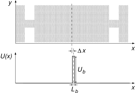
In our study, we consider monolayer graphene ribbons with armchair edges. Two constrictions, created, for example, by etching, separate a part of the ribbon, representing the cavity, from the entrance and exit leads. The cavity is partitioned into two dots by a potential barrier, which, for numerical convenience, we consider to be rectangular. It could be obtained by etching and/or with negatively biased gates located at a certain distance from the graphene ribbon. From a practical point of view, the unavoidable asymmetries in the geometry of the double dot deriving from the impossibility to control the atomic details of the device could be overcome by means of a proper calibration procedure, based on depletion gates, in analogy with what has been proposed in Ref. jap for cavities defined in the 2DEG of semiconductor heterostructures.
A sketch of the simulated structure is shown in Fig. 1.
The overall wave function of graphene can be written as kp
| (1) |
where and represent the positions of the carbon atoms on the two sublattices and and is the atomic orbital of each carbon atom. Using an envelope function approach, the wave functions and corresponding to the two sublattices can be expressed as
| (2) |
where the envelope functions (corresponding to the two inequivalent Dirac points and sublattices ) have to satisfy the Dirac-Weyl equation
| (3) |
with boundary conditions depending on the shape of the particular graphene structure. Here, , , the ’s are the Pauli matrices, is the injection energy, is the potential energy, and (with the reduced Planck constant and the graphene Fermi velocity).
In analogy with Ref. icnf2013 , we have partitioned the considered device into transversal sections of constant width, within each of which the potential energy is approximately constant in the transport direction . Therefore, each of these sections is an armchair graphene ribbon with the potential varying only in the transverse direction and with its effective edges (the rows of lattice points immediately outside the ribbon) at and . Since at these two edges points of both the and the sublattice are present, along them we have to enforce the vanishing of both and . Moreover, exploiting the translational invariance along , we can write each envelope function in the form kp ; brey , where is the wave vector in the transport direction. Therefore the problem to be solved becomes
| (4) |
where , , and .
We have verified that the solution of this problem in the direct space with standard discretization techniques yields a large number of spurious solutions or the appearance of an unphysical degeneracy. The adoption of the Stacey discretization scheme allows to overcome these problems stacey ; tworzydlo but still represents an inefficient solution method, because it requires a quite dense discretization grid in order to achieve a satisfactory representation of the derivatives. Therefore, we have used a different solution technique: we have first introduced, over a doubled domain , the new functions , defined as in and as in , and . In terms of these functions, the system (4) becomes
| (5) |
where ( being the graphene lattice constant) and the boundary condition is periodic for the function iwce2010 ; pt . We have solved this new problem in the Fourier domain (but we could equivalently operate in the direct domain using a basis of sinc-related functions sinc ). From the solution of this problem, we have obtained the longitudinal wave vectors and the transverse component of the envelope function in each transverse section.
The interfaces between the transversal sections are potential and/or geometrical discontinuities (each geometrical discontinuity includes also zigzag transversal segments, which are part of the boundary of the overall graphene structure).
We have computed the scattering matrix of the region straddling each discontinuity by enforcing the continuity of the wave function between the left and right side. In general, this has to be done both for the and for the sublattices (i.e., both for and for ). We have projected these continuity equations onto a set of functions (with an integer number), which represent a basis for the transverse components of the envelope functions that we have found, obtaining in this way a linear system in the reflection and transmission coefficients.
The interface between two graphene sections of different width includes also sections of zigzag boundary. Along such sections we have to enforce the vanishing of the wave function only for one sublattice (exactly as it is necessary to do along the edges of zigzag ribbons brey ). This is obtained simply by projecting the continuity equation for that sublattice onto the sine functions corresponding to the wider graphene section and the continuity equation for the other sublattice onto the sine functions corresponding to the narrower graphene section.
Once we have obtained the scattering matrices of all the regions, we can recursively compose them, in such a way as to obtain the overall scattering matrix and, from it, the transmission matrix of the complete device. Finally, we compute the conductance from the transmission matrix using the Landauer-Büttiker formula buttiker
| (6) |
where is the modulus of the electron charge, is Planck’s constant, and the are the eigenvalues of the matrix (where is the global transmission matrix).
The results that we show in the following have been obtained for zero temperature and vanishing bias voltage, i.e., without any average over the injection energy. For finite temperatures, and room temperature, in particular, there would be some smoothing, due to energy averaging, and additional, inelastic scattering due to phonons. Indeed, for the considered structure (to be fabricated with graphene on a boron nitride substrate, as it will be discussed in the next section), the scattering due to impurities included in our model is expected to be of the same order of magnitude as that due to phonon scattering at 300 K; ferrypap ; zomer therefore, our results should represent a reasonable estimate also for room temperature operation.
III Numerical results

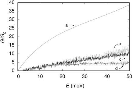
We start by studying the conductance of the barrier alone, without the constrictions defining the cavity. In Fig. 2, we report the conductance obtained for a 2 m wide (solid curve) or 1 m (dashed curve) wide ribbon with a transverse barrier (with thickness 30 nm) extending across the whole wire width, as a function of the barrier height , for a carrier injection energy equal to 40 meV. As expected, nguyen we observe an oscillating behavior, with complete barrier transparency, when (with an integer number), which corresponds (neglecting the transverse wave vector) to the condition of the injection energy being approximately equal to the energy of a hole state quasi-confined inside the barrier.
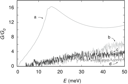
We have then simulated the transport behavior of a 4 m long and 2 m wide graphene cavity connected to the input and output leads by two 400 nm wide constrictions and divided into two square dots by a 30 nm thick and 50 meV high tunnel barrier. More precisely, the wide and narrow parts of the cavity are armchair graphene ribbons with 16263 and 3253 dimer lines across their width, respectively, both corresponding to ribbons with a semiconducting behavior.

In Fig. 3, we report the conductance, as a function of the injection energy, of the tunnel barrier alone (grey solid curve a), of the cavity alone (grey dotted curve b), of the cavity with the barrier exactly in the middle (black solid curve c), and of the cavity with the barrier shifted from the center by 10 nm (black dotted curve d). Comparing these results with those obtained in the case of semiconductor heterostructures, jce ; prl ; jap we see that here the presence of two constrictions symmetrically located around the barrier does not enhance its transmission, but rather decreases it by a significant amount. However, if the barrier is shifted away from the center of the cavity (i.e., the symmetry is broken), the transmission exhibits a clear decrease, even though this effect is now apparent only for higher energies and is less dramatic than in semiconductor heterostructures.
Indeed, as we observed in Refs. prl and jap , the dependence of the conductance of a double dot on symmetry increases as the barrier is made less transparent. Since in graphene the transparency of the barrier is enhanced by Klein tunneling, the dependence of conductance on symmetry is weaker than in semiconductor heterostructures. Also the fact that conductance is never increased over that of the barrier alone (as it is instead observed in analogous devices implemented with III-V material systems) could be explained by the presence of Klein tunneling, which significantly increases the transmission for electrons, in particular those that impinge orthogonally against the barrier.
In Fig. 4 we show the dependence of the conductance of the double dot on the shift of the barrier from the center, keeping the injection energy constant at 40 meV. As we see, the conductance has a maximum when the barrier is exactly at the center of the cavity, while it decreases as the barrier is shifted away. The presence of a smaller local maximum for a barrier shift of about 8.3 nm can be attributed to the constructive interference of a small subset of transmission paths for that barrier position.
Analogous simulations have been performed also for a very similar structure, in which, however, the wide and narrow parts of the device are 16262 and 3254 dimer line wide, respectively, and thus are characterized by a metallic behavior. The results we have obtained are very similar to those shown in Figs. 3 and 4. This demonstrates that the phenomenon does not depend on the exact number of atoms across the width of the wire, and in particular on the semiconducting or metallic nature of the graphene sections.
We have investigated how the observed effect depends on cavity size, by performing simulations for smaller cavities. Here we report a couple of meaningful examples: a m2 cavity and a nm2 cavity. It would be interesting to reduce the size of the cavity to have less demanding requirements in terms of mean free path, but, on the other hand, the magnitude of the conductance modulation is reduced, too, in smaller cavities.
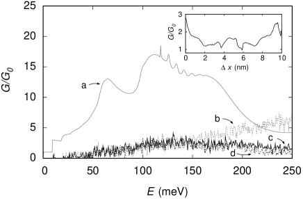
For the m long and m wide cavity, with 200 nm wide constrictions and a meV high and nm thick tunnel barrier, in Fig. 5 we report the conductance of the barrier and of the cavity alone, as well as of the cavity with the barrier exactly in the middle and shifted 10 nm away from the center. Notice that the transmission of the barrier has a maximum when the injection energy is approximately meV (i.e., when the energy of the impinging electron states corresponds to that of the hole states inside the barrier). In Fig. 6, we report the conductance of this structure as a function of the shift of the barrier position from the center of the cavity, which exhibits a behavior substantially analogous to that of the larger cavity we previously investigated.

For the 400 nm long and 200 nm wide cavity, we have considered 40 nm wide constrictions and a 30 nm thick and 250 meV high tunnel barrier. In this case, we have increased the range of considered injection energies (and, as a consequence, the height of the barrier) in order to have a sufficiently large number of propagating modes (the effect we are interested in can be observed only in the presence of a relatively large number of modes, also in the previously studied cavities). We report results for the 400 nm 200 nm cavity in Fig. 7: in this case, the conductance does not exhibit a significant dependence on the symmetry of the structure for any injection energy. This is clear also from the inset of Fig. 7, where we show the conductance as a function of barrier shift, for an injection energy of 200 meV: the conductance decreases monotonically only in a reduced interval near the origin.
This confirms a trend that we had already observed for heterostructure-based cavities jap : there is an optimal cavity size, because on the one hand it is better to have a large cavity, in order to enhance the effect, on the other hand too large a cavity leads to long trajectories, which involve too strong inelastic scattering.

Finally, we have studied the influence of potential disorder on the observed effect. In particular, here we show the results that we have obtained for a 2 m long and 1 m wide cavity with 200 nm wide constrictions and a 30 nm thick and 50 meV high tunnel barrier. To the potential within the cavity, we have added disorder in the form of a sum of randomly distributed Gaussian contributions (each with a half-width at half-maximum equal to 5 nm) with a density equal to cm-2. In Fig. 8, we report the conductance as a function of the barrier shift, both in the absence of disorder (solid curve) and in the presence of potential fluctuations with different amplitude ranges. The amplitude of the Gaussians is uniformly distributed within each considered range. The weakest disorder we have considered is within the range , which is narrow, but still realistic, corresponding to that reported for graphene on a hexagonal boron nitride substrate xue ; morgenstern . Results for this disorder level are reported with a dashed curve in Fig. 8: the main conductance modulation effect does survive in this condition. The effect is instead suppressed if we consider wider amplitude ranges, e.g., (dashed-dotted line) and (dotted line), which are closer to the values measured on samples of graphene on SiO2 substrates droscher ; morgenstern .
IV Conclusion
Our numerical results have shown that the conductance of a graphene double dot strongly depends on the symmetry of the structure, exhibiting a maximum when the tunnel barrier separating the two halves is exactly in the middle. This effect can be observed for cavities with a size in the few-micron range, does not depend strongly on the width of the dots or on the thickness of the barrier, and, in addition, survives in the presence of a moderate level of disorder. Overall, in graphene this phenomenon is less dramatic than in heterostructure-based double dots and, in particular, it does not include the enhancement of the conductance over that of the barrier alone prl .
Our analysis in terms of disorder amplitude reveals that for an experimental verification of this effect in graphene it will be necessary to use material of very high quality, deposited on substrates, such as boron nitride, for which potential fluctuations of the order of 10 meV or less have been estimated.
Due to the fact that for such material room temperature phonon scattering (which is not included in our calculation) is expected to be of the same order of magnitude as impurity scattering, there is hope for a working room temperature demonstration of the effect, and therefore for the practical implementation of position or magnetic field sensors, which would be unlikely with III-V semiconductors, whose mobility is degraded too much by the phonon contribution.
References
- (1) B. J. van Wees, H. van Houten, C. W. J. Beenakker, J. G. Williamson, L. P. Kouwenhoven, D. van der Marel, and C. T. Foxon, Phys. Rev. Lett. 60, 848 (1988).
- (2) D. A. Wharam, T. J. Thornton, R. Newbury, M. Pepper, H. Ahmed, J. E. F. Frost, D. G. Hasko, D. C. Peacock, D. A. Ritchie, and G. A. C. Jones, J. Phys. C: Solid State Phys. 21, L209 (1988).
- (3) U. Meirav, M. A. Kastner, and S. J. Wind, Phys. Rev. Lett. 65, 771 (1990).
- (4) M. Field, C. G. Smith, M. Pepper, D. A. Ritchie, J. E. F. Frost, G. A. C. Jones, and D. G. Hasko, Phys. Rev. Lett. 70, 1311 (1993).
- (5) R. de Picciotto, M. Reznikov, M. Heiblum, V. Umansky, G. Bunin, and D. Mahalu, Nature 389, 162 (1997).
- (6) A. Kumar, L. Saminadayar, D. C. Glattli, Y. Jin, and B. Etienne, Phys. Rev. Lett. 76, 2778 (1996).
- (7) V. Mitin, V. Kochelap, and M. A. Stroscio, Quantum Heterostructures. Microelectronics and Optoelectronics (Cambridge University Press, Cambridge, 1999).
- (8) P. Roblin and H. Rohdin, High-Speed Heterostructure Devices (Cambridge Univ. Press, Cambridge, 2002).
- (9) D. K. Ferry, S. M. Goodnick, and J. Bird, Transport in Nanostructures (Cambridge Univ. Press, Cambridge, 2009).
- (10) H. Ehrenreich and D. Turnbull, Solid State Physics: Advances in Research and Applications 44 (Semiconductor Heterostructures and Nanostructures) (Academic Press, Boston, 1991).
- (11) P. Harrison, Quantum Wells, Wires and Dots: Theoretical and Computational Physics of Semiconductor Nanostructures (Wiley, Chichester, 2005).
- (12) P. Marconcini, M. Macucci, G. Iannaccone, B. Pellegrini, and G. Marola, Europhys Lett. 73, 574 (2006).
- (13) P. Marconcini, M. Macucci, G. Iannaccone, and B. Pellegrini, Phys. Rev. B 79, 241307(R) (2009).
- (14) P. Marconcini, M. Macucci, D. Logoteta, and M. Totaro, Fluct. Noise Lett. 11, 1240012 (2012).
- (15) P. Marconcini, M. Totaro, G. Basso, and M. Macucci, AIP Advances 3, 062131 (2013).
- (16) M. Macucci and P. Marconcini, Journal of Computational Electronics 6, 203 (2007).
- (17) R. S. Whitney, P. Marconcini, and M. Macucci, Phys. Rev. Lett. 102, 186802 (2009).
- (18) S. Oberholzer, E. V. Sukhorukov, C. Strunk, C. Schönenberger, T. Heinzel, and M. Holland, Phys. Rev. Lett. 86, 2114 (2001).
- (19) M. Totaro, P. Marconcini, D. Logoteta, M. Macucci, and R. S. Whitney, J. Appl. Phys. 107, 043708 (2010).
- (20) K. S. Novoselov, A. K. Geim, S. V. Morozov, D. Jiang, Y. Zhang, S. V. Dubonos, I. V. Grigorieva, and A. A. Firsov, Science 306, 666 (2004).
- (21) A. K. Geim and K. S. Novoselov, Nature Materials 6, 183 (2007).
- (22) A. K. Geim, Science 324, 1530 (2009).
- (23) A. H. Castro Neto, F. Guinea, N. M. R. Peres, K. S. Novoselov, and A. K. Geim, Rev. Mod. Phys. 81, 109 (2009).
- (24) D. R. Cooper, B. D’Anjou, N. Ghattamaneni, B. Harack, M. Hilke, A. Horth, N. Majlis, M. Massicotte, L. Vandsburger, E. Whiteway, and V. Yu, “Experimental Review of Graphene,” ISRN Condensed Matter Phys. 2012, 501686 (2012).
- (25) S. Mikhailov, Physics and Applications of Graphene (InTech, Rijeka, 2011).
- (26) M. R. Connolly, R. K. Puddy, D. Logoteta, P. Marconcini, M. Roy, J. P. Griffiths, G. A. C. Jones, P. A. Maksym, M. Macucci, and C. G. Smith, Nano Lett. 12, 5448 (2012).
- (27) D. Logoteta, P. Marconcini, M. R. Connolly, C. G. Smith, and M. Macucci, “Numerical simulation of scanning gate spectroscopy in bilayer graphene in the Quantum Hall regime,” in Proceedings of IWCE 2012 (IEEE Conference Proceedings) (2012), art. number 6242841, DOI: 10.1109/IWCE.2012.6242841.
- (28) P. Marconcini, A. Cresti, F. Triozon, G. Fiori, B. Biel, Y.-M. Niquet, M. Macucci, and S. Roche, ACS Nano 6, 7942 (2012).
- (29) P. Marconcini, A. Cresti, F. Triozon, G. Fiori, B. Biel, Y.-M. Niquet, M. Macucci, and S. Roche, “Electron-hole transport asymmetry in Boron-doped Graphene Field Effect Transistors,” in Proceedings of IWCE 2012 (IEEE Conference Proceedings) (2012), art. number 6242844, DOI: 10.1109/IWCE.2012.6242844.
- (30) H. Raza, Graphene Nanoelectronics: Metrology, Synthesis, Properties and Applications (Springer, Heidelberg, 2012).
- (31) F. Schwierz, Nature Nanotech. 5, 487 (2010).
- (32) G. Iannaccone, G. Fiori, M. Macucci, P. Michetti, M. Cheli, A. Betti, and P. Marconcini, “Perspectives of graphene nanoelectronics: probing technological options with modeling,” in Proceedings of IEDM 2009 (IEEE Conference Proceedings) (2009), p. 245, DOI: 10.1109/IEDM.2009.5424376.
- (33) K. S. Novoselov, V. I. Fal’ko, L. Colombo, P. R. Gellert, M. G. Schwab, and K. Kim, Nature 490, 192 (2012).
- (34) T. Ando, J. Phys. Soc. Jpn. 74, 777 (2005).
- (35) P. Marconcini and M. Macucci, “The kp method and its application to graphene, carbon nanotubes and graphene nanoribbons: the Dirac equation,” La Rivista del Nuovo Cimento 34, 489 (2011).
- (36) M. I. Katsnelson and K. S. Novoselov, Solid State Commun. 143, 3 (2007).
- (37) M. I. Katsnelson, K. S. Novoselov, and A. K. Geim, Nature Physics 2, 620 (2006).
- (38) C. W. J. Beenakker, Rev. Mod. Phys. 80, 1337 (2008).
- (39) D. Logoteta, P. Marconcini, and M. Macucci, “Numerical simulation of shot noise in disordered graphene,” in Proceedings of ICNF 2013 (IEEE Conference Proceedings) (2013), art. number 6578889, DOI: 10.1109/ICNF.2013.6578889.
- (40) L. Brey and H. A. Fertig, Phys. Rev. B 73, 235411 (2006).
- (41) R. Stacey, Phys. Rev. D 26, 468 (1982).
- (42) J. Tworzydło, C. W. Groth, and C. W. J. Beenakker, Phys. Rev. B 78, 235438 (2008).
- (43) P. Marconcini, D. Logoteta, M. Fagotti, and M. Macucci, “Numerical solution of the Dirac equation for an armchair graphene nanoribbon in the presence of a transversally variable potential,” in Proceedings of IWCE 2010 (IEEE Conference Proceedings) (2010), p. 53, DOI: 10.1109/IWCE.2010.5677938.
- (44) M. Fagotti, C. Bonati, D. Logoteta, P. Marconcini, and M. Macucci, Phys. Rev. B 83, 241406(R) (2011).
- (45) P. Marconcini, D. Logoteta, and M. Macucci, J. Appl. Phys. 114, 173707 (2013).
- (46) M. Büttiker, Phys. Rev. Lett. 65, 2901 (1990).
- (47) D. K. Ferry, “Transport in Graphene on BN and SiC,” in Proceedings of IEEE-NANO 2012 (IEEE Conference Proceedings) (2012), art. number 6322126, DOI: 10.1109/NANO.2012.6322126.
- (48) P. J. Zomer, S. P. Dash, N. Tombros, and B. J. van Wees, Appl. Phys. Lett. 99, 232104 (2011).
- (49) V.-H. Nguyen, “Electronic transport and spin polarization effects in graphene nanostructures,” Ph.D. thesis, Institut d’Electronique Fondamentale, Université Paris Sud, Orsay, France, 2010.
- (50) J. Xue, J. Sanchez-Yamagishi, D. Bulmash, P. Jacquod, A. Deshpande, K. Watanabe, T. Taniguchi, P. Jarillo-Herrero, and B. J. LeRoy, Nature Mater. 10, 282 (2011).
- (51) M. Morgenstern, Phys. Status Solidi B 248, 2423 (2011).
- (52) S. Dröscher, P. Roulleau, F. Molitor, P. Studerus, C. Stampfer, K. Ensslin, and T. Ihn, Appl. Phys. Lett. 96, 152104 (2010).