Tunneling spectroscopy of superconducting MoN and NbTiN grown by atomic layer deposition
Abstract
A tunneling spectroscopy study is presented of superconducting MoN and Nb0.8Ti0.2N thin films grown by atomic layer deposition (ALD). The films exhibited a superconducting gap of 2 meV and 2.4 meV respectively with a corresponding critical temperature of 11.5K and 13.4K, among the highest reported values achieved by the ALD technique. Tunnel junctions were obtained using a mechanical contact method with a Au tip. While the native oxides of these films provided poor tunnel barriers, high quality tunnel junctions with low zero bias conductance (below 10%) were obtained using an artificial tunnel barrier of Al2O3 on the film’s surface grown by ALD. We find a large critical current density on the order of A/cm2 at for a 60nm MoN film and demonstrate conformal coating capabilities of ALD onto high aspect ratio geometries. These results suggest the ALD technique offers significant promise for thin film superconducting device applications.
Superconducting nitride alloys make excellent candidates for device applications due to their relatively high critical temperature and stability at ambient atmosphere. These characteristics suggest the opportunity for increased performance and efficiency over commonly used niobium. However, challenges and limitations in common fabrication techniques can reduce the application possibilities. Reactive magnetron sputtering is the most commonly used deposition technique that has produced high quality superconducting thin films of niobium based nitrides.van Dover, Bacon, and Sinclair (1982); Bacon et al. (1983); Thakoor et al. (1985) While molybdenum based superconducting nitrides have also been achieved through sputteringIhara et al. (1985) or chemical solutionZhang et al. (2011) techniques, they require a high temperature (700∘C) and/or high pressure annealing process to achieve a critical temperature greater than that of niobium. Various other techniques such as chemical vapor deposition,Shi et al. (1988); *GaninJSSC2006 pulsed laser depositionInumaru, Baba, and Yamanaka (2005); *InumaruPRB2006 and molecular beam epitaxyInumaru, Baba, and Yamanaka (2006b) have produced superconducting molybdenum nitrides, but have failed to even reach 9K. Sputtering methods are generally limited to planar geometries making it very difficult for complex geometry applications such as superconducting radio-frequency (SRF) cavities or superconducting magnets. Additionally, for applications requiring thin pin-hole free insulating barriers such as superconductor-insulator-superconductor (SIS) tunnel junction mixers for terahertz frequencies,Uzawa, Wang, and Kawakami (1998); *GundlachSST2000; *IosadASIT2001 sputtering processes can be quite challenging.
Atomic layer deposition (ALD) is a highly scalable technique that utilizes sequential self-limiting surface chemical reactions to deposit material in a layer-by-layer fashion.Ritala, M. and Leskela, M (2001); Puurunen (2005) ALD provides several advantages over traditional growth methods, including atomic-scale uniformity over large areas, unmatched conformity over complex-shaped substrates, and deposition temperatures well below those often required by other techniques. ALD has previously demonstrated the ability to grow superconducting filmsKlug et al. (2011); *ProslierJPCC2011 and nitride based thin films in particular.Hiltunen et al. (1988) Currently, reports on the superconducting properties of ALD films with Tc’s above 9K have been limited to standard resistance and susceptibility measurements. The bulk of the letter will focus on the characterization of the superconducting properties of Nb0.8Ti0.2N and MoN thin films grown by ALD through the use of electron tunneling spectroscopy. We demonstrate the ability to create artificial tunnel barriers with ALD, with potential applications to devices based on SIS tunnel junctions. Finally, critical current density measurements are performed for MoN. The high value along with the conformal deposition capabilities of ALD thin films are relevant to complex geometry device applications.

Point contact tunneling (PCT) spectroscopyOzyuzer, Zasadzinski, and Gray (1998) is a powerful tool for studying superconductors as the measure of the current flowing between the normal metal (tip) and the superconductor (sample) under a difference of potential allows for a direct measurement of the surface superconducting properties. Using the modified Blonder-Tinkham-Klapwijk (BTK) theoryBlonder, Tinkham, and Klapwijk (1982); *DynesPRL1978 we are able to extract the superconducting gap , barrier strength and phenomenological quasi-particle lifetime broadening parameter from fits of the differential conductance . In the tunnel regime (), the differential conductance is directly proportional to the superconducting density of states, , through the relation
| (1) |
where is the Fermi function. In our setup, the point contact junction is made with the sample by approaching the surface with a sharpened gold tip to create a SIN (superconductor-insulator-normal) junction where an oxide layer serves as the insulator. The tip-sample separation is controlled through the use of a differential screw while mechanical hysteresis of the tip motion allows for probing slightly different regions of the surface and obtaining statistics of the sample’s superconducting properties. A homemade analog sweep generator was combined with a lock-in amplifier to simultaneously measure the and spectra of the junction.
In general, we use the formation of a native oxide barrier at the surface of the sample as a natural barrier to achieve a SIN tunnel junction with the point contact technique. However, the nitride superconductors measured in this work do not readily form a sufficient insulating oxide layer, requiring the introduction of an artificial barrier in order to reach the tunneling regime. Aluminum oxide was selected as the tunneling barrierBelkin et al. (2010); *ProslierAPL2008 for several reasons. From a point contact standpoint, Al2O3 is a well studied and commonly used oxide barrier that has produced high quality planar tunnel junctions.Zasadzinski et al. (1982) Additionally, amorphous Al2O3 can be grown at temperatures as low as 33∘C using ALD,Groner et al. (2004) making it a natural choice to achieve a pin-hole free insulating layer with minimal possibility of damaging or diffusing into delicate substrates. For this study, the artificial tunnel barrier was not deposited in situ in order to establish the efficacy of the artificial barrier. After establishing a baseline for PCT measurements of the bare films, a thin aluminum oxide barrier (2-3 nm) was deposited at 85∘C using Al(CH3)3 and H2O precursors in a commercial Savannah S100 ALD system.
The nitride films were deposited on various substrates at 450∘C in a custom-built hot-walled viscous flow reactor with details of the deposition described elsewhere.Klug et al. (2013); *ElamRSI2002 A 60nm thick MoN film was deposited using a binary process using MoCl5 and NH3 precursors and a 45nm thick film of Nb0.8Ti0.2N was deposited using a NbN:TiN ALD cycle ratio of 1:2. In both cases, growth of the superconducting layer was preceded in situ by deposition of a 10-20 nm thick AlN buffer layer in order to improve the film nucleation and crystallinity. AlN was grown by ALD using AlCl3 and NH3 precursors at 450∘C.
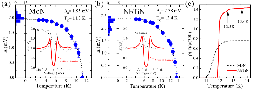
Approximately 35-40 junctions were measured for each sample after the deposition of aluminum oxide to obtain reasonable statistics of the superconducting parameters. For both films, we obtain remarkable improvement in the zero bias conductance (ZBC) after the deposition of the artificial barrier and are able to measure high quality tunnel junctions. Prior to the aluminum oxide deposition, we did not reach the tunnel regime for either film as seen by the dotted curves in the insets of Fig. 1(a-b). Here the ZBC is nearly equal to that at high bias indicating that we are somewhere between tunneling and Andreev reflection where for both films. Looking now at the solid curves shown in the insets of Fig. 1(a-b), one sees the artificial barrier greatly decreases the ZBC to approximately (or below) 10% of the high bias value allowing us to reach the tunneling regime where . This trend has been measured reproducibly for all the junctions and is a clear indication of the the effectiveness and homogeneity of an ALD deposited artificial tunnel barrier.
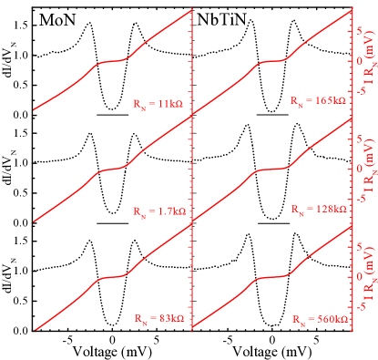
A summary of the PCT measurements for the MoN film are shown in Fig. 1(a). On the left, a histogram of the gap statistics show a single gap value of 2.020.25meV and indicates that we have homogeneous surface superconducting properties. In the main plot of of Fig. 1(a) is shown the measured local gap temperature dependence of a tunnel junction and the fit results according to the BCS temperature dependence (dashed curve) for an s-wave superconductor. Here is found a local gap value of meV and a junction of 11.3K resulting in the ratio =4. The local is consistent with the bulk of 11.50.7K measured by standard four wire transport (dashed curve in Fig. 1(c)) and using the bulk values, the ratio =4.1. In the left panel of Fig. 2 are shown (solid red) and normalized (dashed) spectra obtained for typical junctions of the MoN film. We consistently find tunnel junctions having a ZBC in the range of 10-20% with reasonably sharp energy gap features. This demonstrates not only the feasibility of the artificial barrier, but also that bulk superconductivity appears at the film surface, without any evidence of proximity effects or other surface degradation.
The same series of measurements were conducted on the NbTiN sample for which a summary of the results is displayed in Fig. 1(b). In the left plot, the histogram of the measured gap values show that there appear to be two peaks in the distribution, one centered at 2.32meV and the other at 1.99meV. We conducted a local measure of (main plot) by PCT near the maximum in the gap distribution and find a of 13.40.05K and a gap of 2.380.03meV resulting in a ratio of 4.1. This result is consistent with the transport measurement where we also have multiple transitions (solid red curve in Fig. 1(c)), the highest at 13.60.15K and the lowest at 11.90.13K. The gap statistics and the transport measurements indicate the presence of multiple phases in the NbxTi1-xN film. The large gap (2.4 meV) with a of 13.4K is measured with a higher probability by PCT and yet appear only weakly in the transport measurement. This observation suggests that the corresponding phase is localized mostly at the surface of the film as disconnected islands, whereas the smaller gap (2 meV) would correspond to the bulk of the film with a of 11.9K resulting in a ratio = 3.9. These inhomogeneities could be due to the more complicated chemistry involved in the deposition leading to a formation of islands with slightly different compositions of the NbxTi1-xN film. Like the MoN film, the NbTiN film also exhibited consistently high quality tunnel junctions with single gap features. In the right panel of Fig. 2, typical and normalized curves are shown having low ZBC (10%) and sharp features that could not be obtained relying on a native oxide formation.

For both films studied in this work, we are able to achieve high quality tunnel junctions on surfaces that do not readily form a strong oxide using an ALD deposited insulator. These results provide strong evidence for the feasibility of using ALD to both grow high quality superconducting films as well as create artificial barriers for improved tunneling measurements. ALD is a strong candidate that could be used instead of or in synergy with conventional deposition techniques for superconducting device applications.

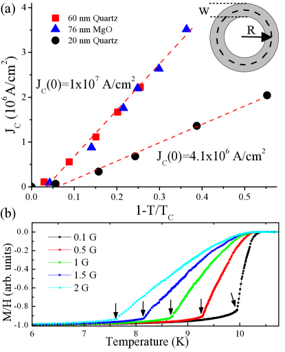
In devices with complex geometries such as SRF cavities and superconducting magnets, the single largest hurdle is the cost incurred using bulk superconducting materials. One straightforward way to drastically reduce the cost of such devices would be to coat inexpensive non-superconducting materials with superconducting films to achieve the same or even improved performance. To investigate the feasibility of ALD deposited superconducting films in these applications, we characterized the critical current density, , and growth characteristics on a high aspect ratio geometry (100:1). We limit this proof-of-principle study only to the MoN thin films due to the simpler nature of the MoN deposition chemistry. Following the inductive technique described in reference 28; *ClausPRB2001, the was extracted from the magnetic response of thin film rings of MoN. Films of different thicknesses, , were deposited on MgO and fused quartz substrates that were then ion-milled into a ring geometry (see Fig. 3(a)) having a central radius, =1.5mm and width, =150m. The induced current in the ring is given by:
| (2) |
where is the applied field. In our geometry we have the simple relation , where is in mT. Using a SQUID (Superconducting QUantum Interference Device) magnetometer, we measured the temperature dependence of the magnetization curves for three different film thicknesses under several applied magnetic fields. At a given temperature, when the critical-current is reached, the applied field fully penetrates the ring resulting in a kink in the magnetization curves as indicated by the arrows in Fig. 3(b). From this, we extracted the critical current density as a function of temperature shown in Fig. 3(a). The results show a remarkable =A/cm2 for a 60nm thin film and only slightly smaller at A/cm2 for a 20nm film. If we consider a copper wire with a diameter of 50m coated with 60nm of MoN, the critical current would be nearly 1 amp at 2K. Scaling up the number of copper wires could then offer the possibility of tremendous current carrying capabilities for superconducting magnet applications.

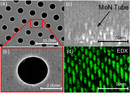
In order to illustrate the conformal deposition capabilities of ALD for potential applications, we deposited 76nm of MoN onto a borosilicate substrate containing a hexagonal pattern of capillary tubes a few microns in diameter and analyzed the deposition using a scanning electron microscope (SEM) equipped with energy dispersive X-ray (EDX) spectroscopy. The measurements reveal a uniform film coating of the surface with no evidence of plugged capillaries (Fig.4(a-b)), indicative of a self-limiting layer-by-layer deposition. A cross section of the sample was obtained by breaking the membrane in half and observing the penetration of the deposition into the capillary tubes. In Fig. 4(c), MoN tubes can be seen sticking out of the broken capillaries approximately 150m below the substrate surface (1mm total substrate thickness). We performed an elemental analysis using EDX where we found these tubes to be composed of molybdenum and nitrogen with a N/Mo ratio of 1.03, confirming a stoichiometric deposition of MoN.
In summary, we have measured high quality tunnel junctions on MoN and NbTiN thin films grown by atomic layer deposition with the application of an artificial tunnel barrier. These films exhibit larger and than that of conventionally used niobium, offering the possibility of improved performance over current niobium-based devices. We have shown that ALD has the capability of coating complex geometries that can have tremendous advantages over conventional deposition techniques. ALD deposited MoN films exhibit a very large critical current density that can be exploited for superconducting magnet architectures. Currently, we are working to further optimize the deposition parameters to increase and incorporate these films into device applications. We are investigating the use of ALD to create in situ SIS tunnel junctions as well as coating normal metals for complex geometry devices.
The authors would like to thank Incom for providing us with the borosilicate substrates. This work was funded by American Recovery and Reinvestment Act (ARRA) thru the US Department of Energy, Office of High Energy Physics Department of Science to Argonne National Laboratory. The author Serdar Altin would like to thank TUḂITAK-BİDEP for financial support during this study. Use of the Center for Nanoscale Materials and the Electron Microscopy Center at Argonne National Laboratory were supported by the U.S. Department of Energy, Office of Science under Contract No. DE-AC02-06CH11357.
References
- van Dover, Bacon, and Sinclair (1982) R. B. van Dover, D. D. Bacon, and W. R. Sinclair, Applied Physics Letters 41, 764 (1982).
- Bacon et al. (1983) D. D. Bacon, A. T. English, S. Nakahara, F. G. Peters, H. Schreiber, W. R. Sinclair, and R. B. van Dover, Journal of Applied Physics 54, 6509 (1983).
- Thakoor et al. (1985) S. Thakoor, J. L. Lamb, A. P. Thakoor, and S. K. Khanna, Journal of Applied Physics 58, 4643 (1985).
- Ihara et al. (1985) H. Ihara, M. Hirabayashi, K. Senzaki, Y. Kimura, and H. Kezuka, Phys. Rev. B 32, 1816–1817 (1985).
- Zhang et al. (2011) Y. Zhang, N. Haberkorn, F. Ronning, H. Wang, N. A. Mara, M. Zhuo, L. Chen, J. H. Lee, K. J. Blackmore, E. Bauer, A. K. Burrell, T. M. McCleskey, M. E. Hawley, R. K. Schulze, L. Civale, T. Tajima, and Q. Jia, Journal of the American Chemical Society 133, 20735 (2011).
- Shi et al. (1988) Y. H. Shi, B. R. Zhao, Y. Y. Zhao, L. Li, and J. R. Liu, Phys. Rev. B 38, 4488–4491 (1988).
- Ganin, Kienle, and Vajenine (2006) A. Y. Ganin, L. Kienle, and G. V. Vajenine, Journal of Solid State Chemistry 179, 2339 (2006).
- Inumaru, Baba, and Yamanaka (2005) K. Inumaru, K. Baba, and S. Yamanaka, Chemistry of Materials 17, 5935 (2005).
- Inumaru, Baba, and Yamanaka (2006a) K. Inumaru, K. Baba, and S. Yamanaka, Phys. Rev. B 73, 052504 (2006a).
- Inumaru, Baba, and Yamanaka (2006b) K. Inumaru, K. Baba, and S. Yamanaka, Applied Surface Science 253, 2863 (2006b).
- Uzawa, Wang, and Kawakami (1998) Y. Uzawa, Z. Wang, and A. Kawakami, Applied Physics Letters 73, 680 (1998).
- Gundlach and Schicke (2000) K. H. Gundlach and M. Schicke, Superconductor Science and Technology 13, R171 (2000).
- Iosad et al. (2001) N. Iosad, V. V. Roddatis, S. N. Polyakov, A. V. Varlashkin, B. D. Jackson, P. Dmitriev, J. Gao, and T. Klapwijk, Applied Superconductivity, IEEE Transactions on 11, 3832 (2001).
- Ritala, M. and Leskela, M (2001) Ritala, M. and Leskela, M, Handbook of Thin Film Materials, edited by Hari Singh Nalwa, Vol. 1 (Academic Press, 2001).
- Puurunen (2005) R. L. Puurunen, Journal of Applied Physics 97, 121301 (2005).
- Klug et al. (2011) J. A. Klug, T. Proslier, J. W. Elam, R. E. Cook, J. M. Hiller, H. Claus, N. G. Becker, and M. J. Pellin, The Journal of Physical Chemistry C 115, 25063 (2011).
- Proslier et al. (2011) T. Proslier, J. A. Klug, J. W. Elam, H. Claus, N. G. Becker, and M. J. Pellin, The Journal of Physical Chemistry C 115, 9477 (2011).
- Hiltunen et al. (1988) L. Hiltunen, M. Leskelä, M. Mäkelä, L. Niinistö, E. Nykänen, and P. Soininen, Thin Solid Films 166, 149 (1988).
- Ozyuzer, Zasadzinski, and Gray (1998) L. Ozyuzer, J. F. Zasadzinski, and K. E. Gray, Cryogenics 38, 911 (1998).
- Blonder, Tinkham, and Klapwijk (1982) G. E. Blonder, M. Tinkham, and T. M. Klapwijk, Phys. Rev. B 25, 4515–4532 (1982).
- Dynes, Narayanamurti, and Garno (1978) R. C. Dynes, V. Narayanamurti, and J. P. Garno, Phys. Rev. Lett. 41, 1509–1512 (1978).
- Belkin et al. (2010) A. Belkin, V. Novosad, M. Iavarone, R. Divan, J. Hiller, T. Proslier, J. E. Pearson, and G. Karapetrov, Applied Physics Letters 96, 092513 (2010).
- Proslier et al. (2008) T. Proslier, J. Zasadzinski, J. Moore, M. Pellin, J. Elam, L. Cooley, C. Antoine, J. Norem, and K. E. Gray, Applied Physics Letters 93, 192504 (2008).
- Zasadzinski et al. (1982) J. Zasadzinski, D. M. Burnell, E. L. Wolf, and G. B. Arnold, Physical Review B 25, 1622 (1982).
- Groner et al. (2004) M. D. Groner, F. H. Fabreguette, J. W. Elam, and S. M. George, Chemistry of Materials 16, 639 (2004).
- Klug et al. (2013) J. A. Klug, N. G. Becker, N. R. Groll, C. Cao, M. S. Weimer, M. J. Pellin, J. F. Zasadzinski, and T. Proslier, Applied Physics Letters 103, 211602 (2013).
- Elam, Groner, and George (2002) J. W. Elam, M. D. Groner, and S. M. George, Review of Scientific Instruments 73, 2981 (2002).
- Herzog et al. (1997) T. Herzog, H. A. Radovan, P. Ziemann, and E. H. Brandt, Physical Review B 56, 2871 (1997).
- Claus et al. (2001) H. Claus, U. Welp, H. Zheng, L. Chen, A. P. Paulikas, B. W. Veal, K. E. Gray, and G. W. Crabtree, Physical Review B 64, 144507 (2001).