Negative quantum capacitance in graphene nanoribbons
with lateral gates
Abstract
We present numerical simulations of the capacitive coupling between graphene nanoribbons of various widths and gate electrodes in different configurations. We compare the influence of lateral metallic or graphene side gate structures on the overall back gate capacitive coupling. Most interestingly, we find a complex interplay between quantum capacitance effects in the graphene nanoribbon and the lateral graphene side gates, giving rise to an unconventional negative quantum capacitance. The emerging non-linear capacitive couplings are investigated in detail. The experimentally relevant relative lever arm, the ratio between the coupling of the different gate structures, is discussed.
pacs:
81.05.ue, 84.32.TtI Introduction
Graphene nanoribbons che07 ; han07 ; li08 ; tod09 ; sta09 ; jia10 ; cai10 are of increasing interest due to their promise of a band gap, overcoming the gapless band structure of truly two-dimensional (2D) graphene kat12 ; guinea_review . In particular, their overall semiconducting behavior allows the fabrication of graphene field-effect transistors wan08 , tunnelling barriers gue11 , and quantum devices ihn10 . First experimental demonstrations of graphene nanoribbon based quantum dots liu09 ; wan13 , double quantum dots liu10 and charge sensors gue08 ; neu13 have been reported in recent years. In most of these quantum devices the local electrostatic tunability of the electrochemical potential along graphene nanoribbons is key for the device functionality. For this purpose, local top-gates and lateral gates, based either on metals or in-plane graphene have been fabricated (see, e.g., Refs. Meric08, ; Williams07, ; Young09, ; Stander09, ). In particular, the 2D nature of graphene makes it straightforward to pattern a number of lateral graphene gates and in-plane charge detectors from the very same graphene sheet as the adjacent top-down fabricated nanoribbon ihn10 ; mol10 . Consequently, a better understanding of the capacitive coupling between nanoribbons (with different widths) and (graphene) gate electrodes is important for device optimization and future graphene-based nanoelectronics. This is particularly true for graphene nanodevices since their Fermi energy is tuned using capacitive coupling. The strength of these couplings, in turn, depends on the density of states (DOS) via quantum capacitance effects lur88 ; john04 . The low DOS close to the Dirac point thus makes graphene a rather unusual gate material with reduced and energy dependent screening properties Fogler07 ; Ghaznavi10 . Graphene sheets have been subject to a large number of theoretical and experimental studies of quantum capacitance effects xia09 ; xia10 ; xu11 ; tahir12 ; parrish12 ; kliros12 ; giannazzo09 ; citeulike:11024917 ; dro10 ; Ilani06 ; Wang13 . Indeed, recent advances allowed experiments based on capacitance measurements to observe such phenomena as Fermi velocity renormalization yu13 , fractional quantum Hall phase transitions fel13 , and Hofstadter’s butterfly hun13 . Furthermore, quantum Hall transport has been used to probe the capacitance profile at graphene edges ver13 . These demonstrations give vested hope that quantum capacitance effects in graphene nanodevices could be exploited in future applications.
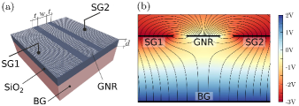
Here we present numerical simulations of the electrostatic capacitive coupling between graphene nanoribbons of different widths and gates in different configurations. In particular we elucidate the influence of metallic and graphene lateral side gate structures (see Fig. 1) on the back gate capacitive coupling. We show that the non-linear capacitive couplings give rise to complex interplay between quantum capacitance effects in the nanoribbon and the gates. Surprisingly, we find the unconventional phenomenon of an effective negative quantum capacitance in nanoribbons with lateral graphene gates. Inclusion of quantum capacitance effects will therefore be essential in reliably interpreting experimental results.
The paper is organized as follows: in Sec. II we briefly introduce the description of quantum capacitance effects on the Thomas-Fermi level and the model system under investigation. Results for graphene nanoribbons with different width, and with metallic and graphene side gates are discussed in Sec. III. Finally, we compare the capacitive coupling between either nanoribbon and back gate or nanoribbon and side gates. We conclude with a short summary.
II Quantum capacitance and model system
Accurate simulations of the influence of side gates require a detailed treatment of the electrostatic problem beyond analytical models available for simple geometries such as the infinitely extended graphene sheet or an isolated nanoribbon.lin08 ; citeulike:11024917 We therefore present a self-contained treatment of the quantum capacitance effect, and present a numerical approach to calculate quantum capacitance effects by coupling the Poisson equation with a Thomas-Fermi approach for the electronic structure. As a first test, we apply our formalism to analytically solvable models.citeulike:11024917
Consider the electrostatic problem of the capacitive coupling between two conductors at different voltages, separated by a medium with permeability . Classically, the resulting electrostatic potential follows the Poisson equation
| (1) |
where is the free charge density and is the relative permittivity. A given potential difference between the two conductors , will lead to a charge accumulation
| (2) |
according to Eq. 1. The classical capacitance then gives the ratio between charge and potential difference,
| (3) |
For nanoscale devices, an additional contribution to the capacitance can arise due to the electronic structure near the Fermi energy of the conductor. This quantum capacitance contribution is related to the additional energy cost for adding electrons to the conductor, which increases if the DOS near the Fermi edge decreases. Graphene with its vanishing DOS at the Dirac point is the prototypical point in case.
Within a Thomas-Fermi approach the local electron density related to the net free charge density through is given by
| (4) |
with the local density of states, and the local Fermi energy. In line with the semiclassical limit underlying the Thomas-Fermi approximation we consider variations only over length scales large compared to the de Broglie wavelength of the electrons. Accordingly, effects such as size quantization features of the graphene nanostructures are neglected in Eq. (4). They could be incorporated, e.g., through a fully self-consistent solution of the Poisson equation and the mean-field Schrödinger equation. However, for the relatively large size of the nanoribbons and in the presence of a small degree of disorder, the deviation from the Thomas-Fermi limit is expected to be small. The leading quantum correction to the classical capacitance should be captured by Eq. (4). Accordingly, the electrochemical potential contains in addition to the electrostatic potential the contribution from the local Fermi energy ,
| (5) |
The solution of the coupled system of Eqs. (1), (4), and (5) allows the calculation of quantum capacitance effects.
Integrating the charge density over the spatial coordinates yields the total capacitance that relates the accumulated charge with the applied potential difference. The total inverse capacitance is given by
| (6) |
where the inverse quantum capacitance reads
| (7) |
and is inversely proportional to the density of states at the Fermi level. For the latter we use in the following the bulk limit in line with the Thomas-Fermi approximation, while the variation of and over the length scale of the device are fully included. The relative importance of quantum capacitance corrections is governed by the ratio
| (8) |
i.e. the ratio of the electrostatically induced charge on the capacitor, , to the total charge near the Fermi edge accessible by a potential difference . In the classical limit, the charge induced on a capacitor at finite voltage is small compared to the total number of electrons at the Fermi level. Conversely, a small density of states at the Fermi level implies a large , and thus a reduction of the total capacitance in Eq. (6).
For infinitely extended two-dimensional graphene, is the energy difference between the highest occupied state on the Dirac cone and the charge neutrality point (i.e. the so-called Dirac point), as a function of the free charge carrier density. We can insert the linear DOS of the Dirac cone, yielding
| (9) |
and
| (10) |
We note that edge roughness or dopants in realistic finite-size structures may strongly influence device properties, in particular the capacitive coupling between nanoribbon and side gates.
Finally, we consider finite temperature effects. Since the energy scales associated with variations of the DOS are of the order of thermal energies, such corrections are important. We therefore investigate the relevance of quantum capacitance corrections at, e.g., room temperature. At finite temperature , the occupation of electronic states is smeared out by the Fermi-Dirac distribution function modifying the expression for the density [Eq. (4)] to
| (11) |
The total charge carrier density (electron and hole charge) for the Dirac cones in graphene then becomes
| (12) |
where is the polylogarithm and . Inverting Eqs. (11) and (12) yields , which can then be used to solve Eq. (5). All data we present in the following are evaluated at room temperature ( K).
III Results and discussion
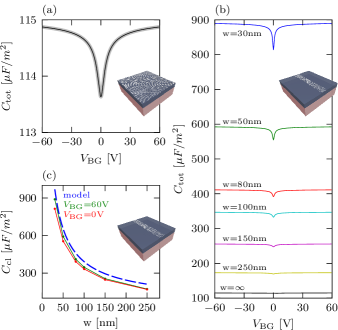
We aim to describe a capacitor formed by a graphene nanoribbon, a metallic back gate and two side gates [see Fig. 1(a)]. The step from idealized, infinite graphene to a nanoribbon with side gates (of possibly different materials and at different potentials) introduces several new device-specific quantum capacitance-related effects. We disentangle them by considering configurations of increasing complexity. To test the validity of our numerical simulation, we start our discussion with the simplest case of an infinitely extended graphene sheet [see Fig. 2(a)]. The nanocapacitor is completed by an infinite back gate at a distance of nm [see Fig. 1(a)], the gap between the two sheets filled with a dielectric substrate, with ; above the nanoribbon is air. The boundary conditions for are given by the potentials applied externally to the different gates. We assume translational symmetry perpendicular to the cross-section shown in Fig. 1(b), thus reducing the calculation to 2D (For technical details, see App. A). As expected, the capacitance decreases at the Dirac point [see Fig. 2(a)] signifying the quantum capacitance effect due to the reduction of the DOS at the Dirac point. Our numerical results agrees (within the numerical accuracy) with analytical models citeulike:11024917 .
III.1 Graphene nanoribbons without side gates
For a nanoribbon of finite width but without side gates, the quantum capacitance effect is substantially increased due to the smaller DOS, leading to a more pronounced quantum capacitance dip for narrower nanoribbons [see Fig. 2(b)]. Consequently, an inclusion of quantum capacitance effects becomes more important for smaller nanonstructures. Concurrently, the classical capacitance per unit area of a nanoribbon increases with decreasing nanoribbon width [see Fig. 2(c)], further amplifying the absolute change in capacitance at the Dirac point. We find good agreement between our simulation and the analytical model discussed by Lin et al. lin08 [see blue dashed line in Fig. 2(c)],
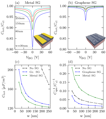
The residual differences are most likely due to the use of spatially constant effective dielectric constants in the analytical model. As discussed above, one can use a full quantum local density of states (LDOS) in Eq. (4) beyond the Thomas-Fermi approximation. Using the quantum LDOS calculated for this geometry we have verified that such a correction yields a negligible change in the capacitance for realistic nanoribbon widths. In line with Eq. (8) we expect the approach of the classical limit with increasing width [Fig. 2(b)] illustrating that as [Fig. 3(d)].
III.2 Graphene nanoribbons with side gates
The introduction of side gates precludes an analytic solution of the problem. Side gates decrease the overall capacitance of the nanoribbon since the classical field-lines further away from the nanoribbon no longer bend towards the nanoribbon (increasing its capacitance), but towards the side gates [see Fig. 1(b)]. Therefore, charge will accumulate at the side gates which decreases the nanoribbon capacitance [compare scale on Figs. 3(c) and 2(c)]. In addition to this classical effect, the different DOS in the graphene nanoribbon and metal side gates further increase the quantum capacitance effect [see Fig. 3(a)]. Put simply, it is energetically much more costly to put electrons into the nanoribbon (due to its small size and the small DOS) than into the metal side gates. A drastically different behavior emerges for graphene side gates [see Figs. 3(b),(c) and (d)], since at the Dirac point the DOS decreases in both the side gates and the nanoribbon simultaneously.
In the experiment, the electrostatic tuning of device properties proceeds by varying the voltages of the side gates relative to that of the back gate. As two prototypical examples, we treat the symmetric (i.e. ) and antisymmetric (i.e. ) voltage configurations. Due to the non-uniform potential distribution , different parts of the device reach the (local) Dirac point at different voltage configurations, namely when locally .
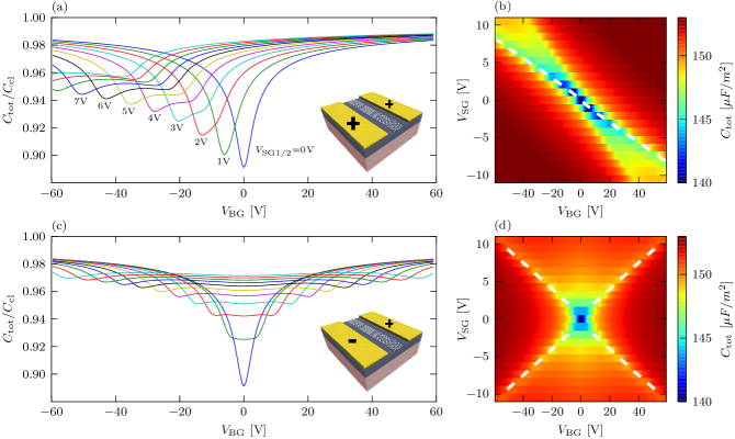
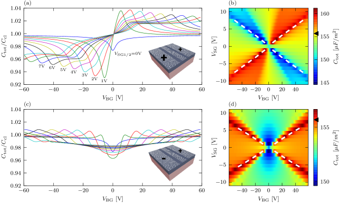
We first consider metal side gates and the symmetric voltage configuration: for positive side gate voltages, the position of the quantum capacitance dip shifts to negative back gate voltages where the side gate influence is compensated [see Figs. 4(a) and 4(b)]. When the energy of the Dirac point is reached in the nanoribbon, the capacitance decreases. The relative depth of the dip depends inversely on the nanoribbon width. For finite voltages , the side gates cause a nonuniform electrostatic potential in the nanoribbon, and the Dirac point is thus reached at different positions in the nanoribbon for different back gate voltages. With increasing side gate voltage, the non-uniformity of the electrostatic potential grows. Consequently, the quantum capacitance dip becomes wider and more shallow: a capacitance landscape in the - plane reveals two lines crossing each other at a small angle [see white lines in Fig. 4(b)] denoting the voltage combinations where no local charge is induced by the gates at either the center of the nanoribbon or its edges. These combinations control the width and shape of the quantum capacitance dip. For the antisymmetric voltage combinations, the situation changes: the width of the dip is now given by the voltage combinations where there is no charge on either the left or the right edge of the nanoribbon [see white lines in Fig. 4(d)], making the change in dip shape more obvious [see Fig. 4(c)].
For graphene side gates, the situation becomes more complicated and novel features emerge: since the DOS of both the nanoribbon and the side gates features minima at the respective Dirac points, quantum capacitance (QC) effects in the nanoribbon and the side gates interact, leading to features beyond the standard “QC dip”. We find an increase in capacitance for larger side gate voltages [i.e. a quantum capacitance peak, see Fig. 5(a)]. This counter-intuitive increase in capacitance due to the limited density of states rather than a reduction arises from the reduced screening response by the side gates which, in turn, restores the capacitance of the nanoribbon. The screening ability of graphene side gates suffers when the Dirac point is reached within the side gates. This loss in screening thus causes a positive peak in the nanoribbon capacitance [see top right in Fig. 5(a)]. These results imply the surprising phenomenon of an effectively negative quantum capacitance. Previously, (narrow) negative quantum capacitance peaks were only observed for graphene heavily doped with Ag adatoms, leading to dispersionless resonant impurity bands near the charge neutrality point Wang13 . The explanation for the splitting and broadening of the QC dips applies analogously to the QC peaks [see dashed lines in Figs. 5(c),(d)].
A comparison of the size of the quantum capacitance dip suggests that the quantum capacitance effect is larger for grounded () metal than grounded graphene side gates [compare Figs. 4(a) and 4(b)]. The observation that the capacitance of the nanoribbon increases when the side gates locally reach their Dirac point offers an additional explanation why the QC dip is deeper for metal side gates than for graphene side gates: since the nanoribbon and the side gates reach the Dirac point at the same potential, the large negative nanoribbon QC dip is superimposed on a positive effective side gate QC peak, and thus, the dip depth is decreased. This overlap can be seen in the capacitance distribution in the - plane [see Figs. 5(c),(d)]: regions of low (blue) and high (red) capacitance converge at the center. As soon as the graphene side gates are at a finite electrostatic potential, the QC peak and the QC dip are shifted relative to each other causing the broadening of the peak and an increase in dip depth.
III.3 Relative lever arms
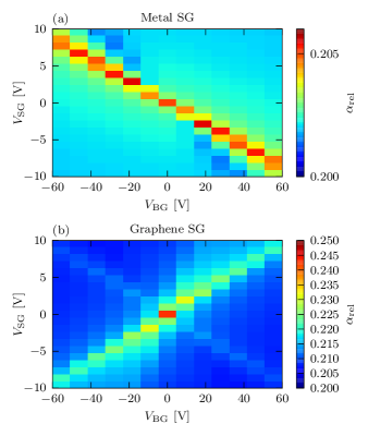
Instead of considering the back gate capacitance as modified by side gates, one may alternatively consider separately the charges induced on the nanoribbon due to finite side gate and the back gate voltages: for each gate, we define a capacitance relating the voltage on the gate to the induced charge on the nanoribbon. A comparison of the relative capacitive couplings, i.e. the ratios of the capacitances, is of great interest for experiments: back gate and side gates usually feature very different coupling coefficients due to the different spatial distance to the nanoribbon. This relative coupling is usually referred to as relative lever arm
| (13) |
Accurate knowledge of is essential for a detailed interpretation of experimental results. Due to quantum capacitance effects, depends on and , as we now investigate in detail. We determine side gate capacitance as and . The relative lever arm as function of and features a substantial energy dependence already for metallic side gates [see Fig. 6(a)]: we find the relative lever arm decreased by roughly three percent around zero carrier density in the nanoribbon. For the case of graphene side gates, we observe a decrease by up to fifteen percent of the relative lever arm along a positive diagonal in the gate voltage plane [highlighted in Fig. 6(b)]. This is of importance as experimental devices often feature side gates and nanoribbon etched from the same graphene sheet.
Interestingly, when comparing our numerical results with the experimental data reported in Ref. mol09, one finds that the experimentally extracted is nearly a factor three larger than our calculation suggests. Since the back gate coupling is well controlled in experiments on large-scale graphene devices, we conjecture that this discrepancy might be related to a significantly reduced side gate coupling in the experiment. In particular, the edges of a realistic experimental nanoribbon device feature edge roughness and uncontrolled edge terminations (both not included in the present model) which may lead to a large local density of states at the edges, and thus to a significant charge accumulation at the edge of the nanoribbon. These charges may partly screen the lateral side gates and therefore increase the measured relative lever arm. Such a screening effect is also consistent with recent observations on hydrofluoric acid (HF) treated graphene nanoribbons where an increased side gate coupling strength has been found after HF dipping dau13 .
IV Summary and outlook
We have shown that side gated graphene nanoribbons exhibit significant variation in capacitance as a function of gate voltages due to classical screening and quantum capacitance effects in the nanoribbon. Both the nanoribbon geometry as well as the presence and material of side gates strongly influence quantum capacitance effects. We find both positive and, surprisingly, unconventional negative quantum capacitance corrections. The former is the usual decrease of total capacitance due to the additional energy required to fill electronic states at a low density of states. The latter occurs due to a decrease of screening by graphene side gates. Since the capacitance of a graphene nanodevice frequently enters in the tuning of the effective energy of electrons in, e.g., transport experiments, inclusion of quantum capacitance effects is critical for the correct interpretation of experimental data. The proposed increase in total capacitance for finite voltage at graphene side gates and the significant change in the relative gate lever arms should be observable experimentally for clean samples.
Acknowledgment
Financial support by the DFG (SPP-1459 and FOR-912), the ERC, the FWF SFB ViCoM, and the JARA Seed fund is gratefully acknowledged.
Appendix A Numerical method
In the following, we provide further technical details on our calculations. We solve the Poisson equation (1) using a finite difference scheme with a grid spacing of 1 nm. Dirichlet boundary conditions are applied to the conducting parts of the system: the lower boundary (where the back gate fixes the potential), the nanoribbon and the side gates. The left, right and top border are best modeled using Neumann boundary conditions, i.e. , as these emulate the infinitely extended system better than Dirichlet boundary conditions. We solve Eqs. (5) for using the charge density for graphene, Eq. (9), in combination with the Poisson equation (1). After the discretization, the resulting nonlinear system of equations can be solved using any nonlinear solver. On all grid points of the graphene parts, there is a difference between the electrochemical potential and the electrostatic potential , given by a discretized version of Eq. (5). Inserting these constraints into the Poisson equation (1) yields
| (14) |
where are the grid points on the graphene parts. This system of equations (, ) is solved for .
Quantum capacitance can also be formulated for a non-local relationship between energy and charge (as required, e.g., for ab-initio calculations of the system)
| (15) |
This equation can be reformulated in terms of charge densities instead of energies by applying the inverse map ,
| (16) |
which gives the charge density, , as a function of the potential and the chemical potential . Assuming a local dependence between and allows replacing the functional formulation (15) by the simpler (5) used in the main text.
References
- (1) Z. Chen et al., Physica E (Amsterdam) 40, 228 (2007).
- (2) M.Y. Han et al., Phys. Rev. Lett. 98, 206805 (2007).
- (3) X. Li, X. Wang, L. Zhang, S. Lee, and H. Dai, Science 319, 1229 (2008).
- (4) K. Todd, H. T. Chou, S. Amasha, and D. Goldhaber-Gordon, Nano Lett. 9, 416 (2009).
- (5) C. Stampfer, et al. Phys. Rev. Lett. 102, 056403 (2009)
- (6) L. Jiao, X. Wang, G. Diankov, H. Wang and H. Dai, Nature Nanotechnology 5, 321 (2010).
- (7) J. Cai, et al., Nature 466, 470 (22 July 2010).
- (8) A. H. C. Neto, F. Guinea, N. M. R. Peres, K. S. Novoselov, and A. K. Geim, Rev. Mod. Phys. 81, 109 (2009).
- (9) M. I. Katsnelson, ”Graphene Carbon in Two Dimensions”, Cambridge Univ. Press May 2012 (ISBN: 9780521195409).
- (10) X. Wang, Y. Ouyang, X. Li, H. Wang, J. Guo, and H. Dai, Phys. Rev. Lett. 100, 206803 (2008).
- (11) J. Güttinger, J. Seif, C. Stampfer, A. Capelli, K. Ensslin, and T. Ihn, Phys. Rev. B 83, 165445 (2011).
- (12) T. Ihn, J. Güttinger, F. Molitor, S. Schnez, E. Schurtenberger, A. Jacobsen, S. Hellmüller, T. Frey, S. Dr scher, C. Stampfer, and K. Ensslin, Materials Today 13, 44 (2010).
- (13) X. Wang, Y. Ouyang, L. Jiao, H. Wang, L. Xie, J. Wu, J. Guo and H. Dai, Nature Nanotechnology 6, 563567 (2011).
- (14) L. Liu, J. B. Oostinga, A. F. Morpurgo, and L. M. K. Vandersypen, Phys. Rev. B 80, 121407 (2009).
- (15) Liu, X. L., D. Hug, et al.. Nano Letters 10, 1623 (2010).
- (16) J. Güttinger, C. Stampfer, S. Hellmuller, F. Molitor, T. Ihn, and K. Ensslin, Appl. Phys. Lett. 93, 212102 (2008).
- (17) C. Neumann, C. Volk, S. Engels, and C. Stampfer, Nanotech. 24, 444001 (2013).
- (18) I. Meric, M. Y. Han, A. F. Young, B. Ozyilmaz, P. Kim, and K. L. Shepard, Nature Nanotech. 3, 654 (2008).
- (19) J. R. Williams, L. DiCarlo, and C. M. Marcus, Science 317, 638 (2007).
- (20) A. F. Young, and P. Kim, Nature Phys. 5, 222 (2009).
- (21) N. Stander, B. Huard, and D. Goldhaber-Gordon, Phys. Rev. Lett. 102, 026807 (2009).
- (22) F. Molitor, C. Stampfer, J. Güttinger, A. Jacobsen, T. Ihn, and K. Ensslin, Semicond. Sci. Technol. 25, 034002 (2010).
- (23) S. Luryi, App. Phys. Lett. 52, 501 (1988).
- (24) D. L. John, L. C. Castro, and D. L. Puffrey, J. App. Phys. 96, 5180 (2004).
- (25) M. M. Fogler, D. S. Novikov, and B. I. Shklovskii, Phys. Rev. B 76, 233402 (2007).
- (26) M. Ghaznavi, Z. L. Mišković, and F. O. Goodman, Phys. Rev. B 81, 085416 (2010).
- (27) J. Xia, F. Chen, J. Li, and N. Tao, Nature Nanotech. 4, 505 (2009).
- (28) J. Xia, F. Chen, J. L. Tedesco, D. K. Gaskill, R. L. Myers-Ward, C. R. Eddy, Jr., D. K. Ferry and N. J. Tao, App. Phys. Lett. 96, 162101 (2010).
- (29) H. Xu, Z. Zhang, and L.-M. Peng, App. Phys. Lett. 98, 133122 (2011).
- (30) M. Tahir, and U. Schwingenschlögl, App. Phys. Lett. 101, 013114 (2012).
- (31) K. N. Parrish, and D. Akinwande, App. Phys. Lett. 101, 053501 (2012).
- (32) G. S. Kliros, Superlattices and Microstructures 52, 1093 (2012).
- (33) F. Giannazzo, S. Sonde, V. Raineri, and E. Riminia, Nano Lett. 9, 23 (2009).
- (34) T. Fang, A. Konar, H. Xing, and D. Jena, App. Phys. Lett. 91, 092109 (2007).
- (35) S. Ilani, L. A K. Donev, M. Kindermann, and P. L. McEuen, Nature Physics 2, 687 (2006).
- (36) L. Wang, et al., Scientific Rep. 3, 2041 (2013).
- (37) S. Dröscher, P. Roulleau, F. Molitor, P. Studerus, C. Stampfer, T. Ihn, and K. Ensslin, Appl. Phys. Lett. 96, 152104 (2010).
- (38) G. L. Yu, R. Jalil, B. Belle, A. S. Mayorov, P. Blake, F. Schedin, S. V. Morozov, L. A. Ponomarenko, F. Chiappini, S. Wiedmann, U. Zeitler, M. I. Katsnelson, A. K. Geim, K. S. Novoselov, and D. C. Elias, Proceedings of the National Academy of Sciences 110, 3282 (2013).
- (39) B. E. Feldman, A. J. Levin, B. Krauss, D. Abanin, B. I. Halperin, J. H. Smet, and A. Yacoby, Phys. Rev. Lett. 111, 076802 (2013).
- (40) B. Hunt, J. D. Sanchez-Yamagishi, A. F. Young, K. Watanabe, T. Taniguchi, P. Moon, M. Koshino, P. Jarillo-Herrero, and R. C. Ashoori, Science 340, 1427 (2013).
- (41) I. J. Vera-Marun, P. J. Zomer, et al., App. Phys. Lett. 102, 013106 (2013).
- (42) Y.-W. Son, and M. L. Cohen, Phys. Rev. Lett. 97, 216803 (2006).
- (43) L. Brey, and H. A. Fertig, Phys. Rev. B 73, 235411 (2006).
- (44) F. Libisch, C. Stampfer, and J. Burgdörfer, Phys. Rev. B 79, 115423 (2009).
- (45) Y.-M. Lin, V. Perebeinos, Z. Chen, and P. Avouris, Phys. Rev. B 78, 161409R (2008).
- (46) D. Subramaniam, F. Libisch, Y. Li, C. Pauly, V. Geringer, R. Reiter, T. Mashoff, M. Liebmann, J. Burgdörfer, C. Busse, T. Michely, R. Mazzarello, M. Pratzer, and M. Morgenstern, Phys. Rev. Lett. 108, 046801 (2012).
- (47) F. Molitor, A. Jacobsen, C. Stampfer, J. Güttinger, T. Ihn, and K. Ensslin, Phys. Rev. B 79 075426 (2009).
- (48) J. Dauber, B. Terrés, C. Volk, S. Trellenkamp, and C. Stampfer, arXiv:1311.5124 (2013).