Now at ]Northrop Grumman Electronic Systems, Linthicum, Maryland 21090, USA
Radio-frequency reflectometry on an undoped AlGaAs/GaAs single electron transistor
Abstract
Radio frequency reflectometry is demonstrated in a sub-micron undoped AlGaAs/GaAs device. Undoped single electron transistors (SETs) are attractive candidates to study single electron phenomena due to their charge stability and robust electronic properties after thermal cycling. However these devices require a large top-gate which is unsuitable for the fast and sensitive radio frequency reflectometry technique. Here we demonstrate rf reflectometry is possible in an undoped SET.
Typically AlGaAs/GaAs systems are realised by modulation doping: a layer of dopants donate excess charge carriers to form a two-dimensional electron gas (2DEG) at the AlGaAs/GaAs interface. Small metallic surface gates are used to define sub-micron features: applying a voltage depletes the 2DEG in the regions under the gates. Modulation doped devices have been integrated into radio-frequency (rf) resonant circuits Schoelkopf1998 , because they have small parasitic capacitances Aassime2001 ; Xue2009 ; Lu2003 which are used to form an resonant circuit when in series with an inductor Schoelkopf1998 . Radio frequency techniques are well suited to exploring phenomena over short time scales, and in modulation doped devices, are central to experiments on qubit entanglement Shulman2012 , noise Fujisawa2000 and spin manipulation Laird2010 .
As an alternative, undoped AlGaAs/GaAs devices can be thought of as the inverse of modulation doped devices. A voltage is applied to an overall top-gate inducing a 2DEG at the AlGaAs/GaAs interface. If the gate is an epitaxial, degenerately doped GaAs layer See2010 then sub-micron structures, such as single electron transistors (SETs), are realised in the 2DEG by etching away small regions of the top-gate Kane1998 ; Klochan2006 ; See2010 (inset to Figure 1). Sub-micron, undoped devices have shown excellent charge stability Klochan2006 , as well as thermal robustness See2010 . In comparison, modulation doped structures can suffer from significant charge noise due to surface gate leakage Buizert2008 ; Pioro-Ladriere2005 ; Cobden1992 and fluctuators in the doping layer Fujisawa2000 ; Kurdak1997 ; Timp1990 . Charge sensing using rf techniques has yet to be used with sub-micron, undoped devices, so probing processes over shorter time scales or fast charge sensing applications, remain unstudied in these systems.
In this paper we address the question: is it possible to use rf reflectometry in a sub-micron, undoped AlGaAs/GaAs SET? The SET is formed in a 2D conducting channel between the source and drain. The 2D leads, as well as the SET are covered by the top-gate. Of central concern is the effect of the large top-gate capacitance on the reflected rf signal. The high-frequency signal could be shunted by the top-gate before reaching the SET, and the large top-gate capacitance could make impedance matching difficult at high frequencies Taskinen2008 . Reducing the top-gate capacitance by shrinking the area may not improve the impedance matching of the circuit. This is because the gated 2DEG acts as a lossy transmission line so that it is the capacitance per unit area, not the total capacitance, which determines the high frequency behaviour of the device Taskinen2008 . Furthermore, as the SET is only a small structure embedded in a 2D conducting channel, it is unclear how sensitive the rf reflectance () will be to the SET resistance.
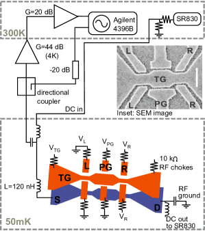
The device used hereSee2010 consists of a 35 nm-thick GaAs n cap (the top-gate) covering the Hall bar and has an area of . Applying a positive voltage to the top-gate controls the electron density, , of the 2DEG which resides 185 nm below the cap, with a geometric capacitance pF to the top-gate. The SET is defined by etching the cap into seven separate gates, labelled left- (L), right- (R), plunger- (PG) and top-gate (TG) as shown in Figure 1, the capacitances are obtained from previous measurements See2010 and are 17.0, 14.5, 20 and 107 aF respectively See2010 . To define the SET a negative voltage is applied to the left-,right- and plunger-gates (, and respectively), thus controlling the tunnel barrier heights and the electron number in the SET. The charging energy of the SET is See2010 .
Low temperature measurements were made in a dilution refrigerator with a 20 mK base temperature. The rf impedance matching network is formed by soldering a inductor onto a printed circuit board (PCB) onto which the sample, bonded in a standard LCC20 chip package, is mounted. The low-frequency lines have rf-chokes soldered in place. Electrical connection between the chip package and PCB is via 20 gold-bonding wires. Figure 1 shows the low-temperature set up for recovering our reflected signal: once the carrier wave is reflected it is separated from the incoming wave via a directional coupler and amplified with a CITLF1 low-noise broadband amplifier (44 dB gain at 20 K) operating at 4 K. This is followed by a 300 K amplification stage (mini-circuits ZFL-1000LN) with 20 dB of gain. The reflected power is measured with an Agilent rf spectrum analyzer or a square-law diode detector (TruPwr Detector, model AD8362), with data averaged over four traces.
The device is first characterised at 4 K in a dedicated rf dip-station with similar wiring to the dilution fridge. To locate the resonant frequency and check is sensitive to the sample resistance, the frequency is swept while is recorded for different values of when the dot is unbiased. Sweeping the frequency yields a sharp resonance at 487 MHz, with a 100 nH, inductor as shown in Figure 2(a). There is a change in of up to 40 dB depending on . The versus frequency curves are determined by the matching of the sample resistance (set here by ) to the circuit. Thus the depth of the minima depends on because the resistance per square of the Hall bar and the SET are controlled by . We have also used a simple lumped-element analysis to model the circuit, as shown by the upper trace in Fig. 2(a). Although this simple model works well for 2D systems Taskinen2008 , it cannot describe the experimental data when the dot is included. More sophisticated modelling should be able to replicate the experimental data, but requires many poorly known parameters, thus limiting the ability to predict the circuit response.
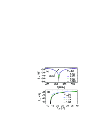
To isolate the effect of the SET we set the signal frequency on resonance (487 MHz) and record versus the four-terminal resistance () across the SET; is changed by sweeping while the top-, left- and right-gate voltages are fixed InfoA . The transfer function is shown in Figure 2(b), where versus is plotted for different values of . For V the circuit is matched at , and shows a change of up to 40 dB as increases. For lower the matching point moves to lower .
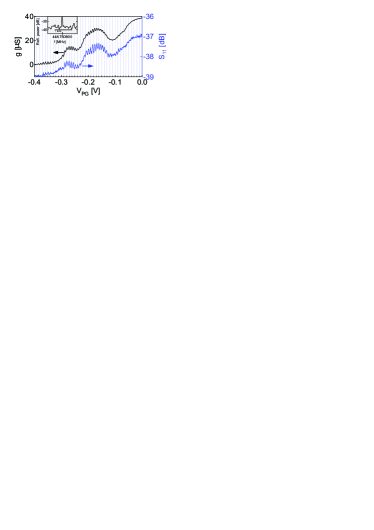
The response of to the SET is best demonstrated by mapping out the conductance oscillations when the SET InfoB is in the Coulomb blockade (CB) regime at low temperature. To improve matching the inductor is changed to 120 nH and the circuit resonance frequency becomes 448.75 MHz. Figure 3 shows the CB oscillations in measured using the low-frequency, two-terminal lockin technique. The CB oscillations are reproduced in when . Here the change in the amplitude of detecting the CB oscillations is small because the sample resistance is larger than . From Figure 2(b) we see if the sample resistance varies between to then changes by dB or less. Thus for a sample resistance between the change in amplitude of is small. The best charge sensitivity is obtained at the maximal slope , thus we configure the dot to sit on the side of a CB peak and apply a small signal excitation () to the top plunger gate at 890 Hz. We obtain a charge sensitivity of with a 3 Hz resolution bandwidth (see inset to Fig.3). We note this charge sensitivity is likely an underestimate, since the SET is still affected by charge noise, as we were limited by gate modulation frequencies below the knee due to low-frequency gate lines. Furthermore the rf matching is far from optimized, so there is much room for improvement which is important for future applications of single shot read-out of undoped quantum dots for spin qubits Barthel2010 . One way to improve the rf matching is to iteratively try different inductors, requiring a thermal cycle with each attempt. Another method is to use a variable capacitor to tune the resonance frequency in situ Muller2010 .
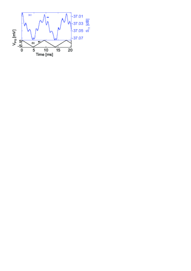
We now demonstrate rf reflectometry by using to track changes in the occupation number of the SET. The SET is configured InfoC in the CB regime while a 15 mV, 110 Hz triangle wave (Figure 4(b)) is applied to the top half of the plunger-gate and is recorded versus time (Figure 4(a)). The smaller peaks in , spaced 1.5 ms apart, show the occupation number of the SET changing as is swept. This corresponds to the SET passing through 1000 CB peaks a second. The frequency applied to the gate is limited by low-pass filters on the gate lines without these the gate could be modulated at much higher frequencies.
In conclusion we have shown rf reflectometry is possible on an undoped, large-area gated, sub-micron SET, despite the predictions of a simple lumped-element circuit model. We observed clear Coulomb blockade in . Future work will include optimising the rf matching and improving the charge sensitivity of the undoped quantum dot.
This work was funded by the Australian Research Council (ARC) DP and FT schemes. A.R.H. acknowledges an ARC Outstanding Researcher Award.
References
- (1) R. J. Schoelkopf, P. Wahlgren, A. A. Kozhevnikov, P. Delsing and D. E Probere, Science 280, 1238 (1998).
- (2) A. Aassime, D. Gunnarsson, K. Bladh, P. Delsing and R. Schoelkopf, Appl. Phys. Lett. 79, 4031 (2001).
- (3) W. W Xue, Z. Ji, F. Pan, J. Stettenheim, M. P. Blencowe and A. J. Rimberg, Nat. Phys. 5, 660 (2009).
- (4) W. Lu, Z. Ji, L. Pfeiffer, K. W. West and A. J. Rimberg, Nature 423, 422 (2003).
- (5) M. D. Shulman, O. E. Dial, S. P. Harvey, H. Bluhm, V. Umansky and A. Yacoby, Science, 336, 202 (2012).
- (6) T. Fujisawa, Y. Hirayama, Appl. Phys. Lett. 77, 543 (2000).
- (7) E. A. Laird, J. M. Taylor, D. P. DiVincenzo, C. M. Marcus, M. P. Hanson and A. C. Gossard, Physical Review B, 82, 075403 (2010).
- (8) A. M. See, O. Klochan, A. R. Hamilton, A. P. Micolich, M. Aagesen and P. E. Lindelof, Appl. Phys. Lett. 96, 112104 (2010).
- (9) B. E. Kane, G. R. Facer, A. S. Dzurak, N. E. Lumpkin, R. G. Clark, L. N. Pfeiffer and K. W. West, Applied Physics Letters, 72, 3506 (1998).
- (10) O. Klochan, W. R. Clarke, R. Danneau, A. P. Micolich, L. H. Ho, A. R. Hamilton, K. Muraki and Y. Hirayama, Appl. Phys. Lett., 89, 092105 (2006).
- (11) C. Buizert, F. H. L. Koppens, M. Pioro-Ladrière, H.-P. Tranitz, I. T. Vink, S. Tarucha, W. Wegscheider and L. M. K. Vandersypen, Phys. Rev. Lett., 101, 226603 (2008).
- (12) M. Pioro-Ladrière, J. H. Davies, A. R. Long, A. S. Sachrajda, L. Gaudreau, P. Zawadzki, J. Lapointe, J. Gupta, Z. Wasilewski and S. Studenikin, Phys. Rev. B, 72, 115331 (2005).
- (13) D. H. Cobden, A. Savchenko, M. Pepper, N. K. Patel, D. A. Ritchie, J. E. F. Frost and, G. A. C. Jones, Phys. Rev. Lett., 69, 502(1992).
- (14) Ç. Kurdak, C.-J. Chen, D. C. Tsui, S. Parihar, S. Lyon and G. W. Weimann, Phys. Rev. B., 56, 9813 (1997).
- (15) G. Timp, R. E. Behringer and J. E. Cunningham, Phys. Rev. B., 42, 9259 (1990).
- (16) L. J. Taskinen, R. P. Starrett, T. P. Martin, A. P. Micolich, A. R. Hamilton, M. Y. Simmons, D. A. Ritchie and M. Pepper, Rev. Sci. Instrum., 79, 123901 (2008).
- (17) See supplementary material for more detail about modeling the circuit using a lumped-element approach. The dot is represented as a variable resistor in parallel with the gate capacitance. The 2DEG is treated as a lossy transmission line following Ref.[16].
- (18) V, V, V.
- (19) The series resistance is due to: rf chokes (); ohmic contacts (); line resistance () and the lock-in input mpedance ().
- (20) The SET was biased with , , and sweeping (. The best results for this configuration were obtained when .
- (21) C. Barthel, M. Kjærgaard, J. Medford, M. Stopa, C. M. Marcus, M. P. Hanson and A. C. Gossard, Physical Review B, 81, 161308(R) (2010).
- (22) T. Müller, B. Küng, S. Hellmüller, P. Studerus, K. Ensslin, T. Ihn, M. Reinwald and W. Wegscheider, Appl. Phys. Lett., 97, 202104 (2010).
- (23) V, V, V and V.