Probing the local environment of two-dimensional ordered vacancy structures in Ga2SeTe2 via aberration-corrected electron microscopy
Abstract
There has been considerable interest in chalcogenide alloys with high concentrations of native vacancies that lead to properties desirable for thermoelectric and phase-change materials. Recently, vacancy ordering has been identified as the mechanism for metal-insulator transitions observed in GeSb2Te4 and an unexpectedly low thermal conductivity in Ga2Te3. Here, we report the direct observation of vacancy ordering in Ga2SeTe2 utilizing aberration-corrected electron microscopy. Images reveal a cation-anion dumbbell inversion associated with the accommodation of vacancy ordering across the entire crystal. The result is a striking example of the interplay between native defects and local structure.
Ga2SeTe2 belongs to a class of III-VI semiconductors with a defect zincblende structure (F3m space group and lattice constant a = 5.77 Å) where, due to a valence mismatch, one third of the cation (group III element) sites are vacant. The high concentration of native vacancies in these materials is responsible for numerous interesting physical properties. Early investigations have shown that vacancies in these materials induce anomalously high radiation stability suitable for semiconductor devices operating in high-flux radiation environments Koshkin:vp ; Koshkin:1976wj ; Gurevich:1995wx . Recently, there has been renewed interest in III-VI semiconductors for thermoelectric and phase-change random access memory applications. Ga2Te3 as a phase-change material, for example, shows better data retention ability, lower power consumption, and higher dynamic electric switching ratios when compared to the better-known Ge2Sb2Te5 Zhu:2010jj . Planar vacancy ordering in Ga2Te3 has been associated with strong phonon scattering, resulting in very low thermal conductivity, showing great potential as a thermoelectric material Kurosaki:2008cj .
Theoretical and experimental investigations have shown that vacancy ordering in phase-change materials acts as a mechanism for metal-insulator transitions, whereby the transition to the metallic state is governed by the formation of ordered vacancy layers from the native vacancy clusters in the insulating state Siegrist:2011ej ; Zhang:2012bp . The result is an effective modification of electronic structure due to intrinsic structural rearrangements, rather than extrinsic compositional changes through doping. It follows that direct observation of such local structural changes, at the atomic level, is paramount for future discovery and understanding of a large class of materials with physical properties amenable to alteration by vacancy ordering. We attempt to do this at the required levels of spatial resolution by employing aberration-corrected scanning transmission electron microscopy (STEM) to image the atomic environment of Ga2SeTe2, with ordered two-dimensional vacancy structures.
Earlier electron microscopy of bulk Ga2Te3 and Ga2Se3 has revealed the presence of a mesoscopic superstructure of two-dimensional ordered vacancies within families of {111} planes Guymont:1992vj ; Kienle:2003eg ; Kim:2011kb . In dark field images, these appear as dark streaks along [111] when viewed in 110 zone axis orientations. Information about these defect structures via dark field imaging at the atomic level remains scarce. Consequently, we probe the environment in the vicinity of these defect structures (which also exist in Ga2SeTe2) by imaging in high-angle annular dark field (HAADF)-STEM utilizing aberration-corrected electron lenses, which drastically improve spatial resolution and image quality Spence:2003 ; Fultz:2007vo ; Williams:2009uy .
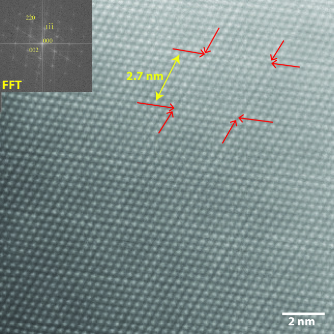
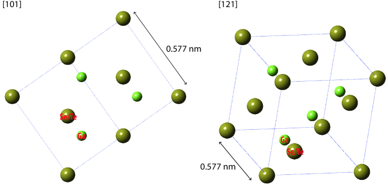
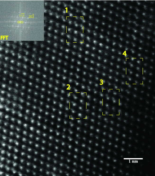
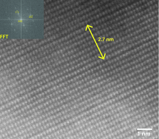
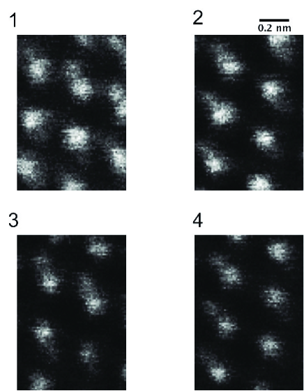
Figure 1 shows the atomic columns of a bulk Ga2SeTe2 crystal along a [110] projection. As expected from prior reports in the literature, we see a periodic contrast variation in the form of dark lines that are parallel to both sets of {111} planes visible in edge-on orientation along this zone axis. The inset Fourier transform of this image confirms the symmetry of atomic column stacking consistent with the face-centered cubic Bravais lattice associated with a zincblende crystal structure (illustrated in Figure 2) and the periodicity of the two-dimensional vacancy ordering. The latter is evidenced by the fine spots at 1/8 the spacing of the {111} planes ( 2.7 nm) along both 111 reciprocal lattice directions in this projection.
A magnified image of the Ga2SeTe2 crystal in the [101] zone axis is shown in Figure 3. Here, we are able to discern the cation-anion dumbbells that are expected in the zincblende lattice when viewed along the [101] projection; the dumbbells are also oriented perpendicular to the long axis created by the 20 reflection in reciprocal space (Figure 3 inset), which is the expected cation-anion orientation along 110 projections. Based on the conventional mechanism of Z-contrast, we expect the brighter spots to represent the higher-Z anions (Te or Se) and the dimmer spots to represent the lower-Z cation (Ga) sites. The dumbbell distance is 0.147 nm in agreement with the predicted value. Additionally, we confirm the pervasiveness of {111} vacancy ordering in the zincblende structure by tilting the Ga2SeTe2 crystal to the [121] zone axis and collecting a dark field image (Figure 4). Consistent with their structural arrangement evident in 110 zone axes, the modulation of vacancy-ordered {111} planes is again repeated at 2.7 nm intervals. However, spatially resolving both cation and anion sites ( 0.085 nm) along 211 zone axes is difficult due to deleterious effects arising from specimen thickness—where it is 15% greater than 110 zone axes thicknesses—and an amorphous layer that covers the crystal, which we had difficulty removing.
Examining the image detail in Figure 3 more carefully, we notice the dumbbell orientation in 110 zone axes projections is inverted across vacancy-ordered planes in a manner analogous to an inversion twin boundary. Four yellow boxes in Figure 3 highlight such inversions. We note that the dumbbell inversion is constant within each domain bounded by the ordered vacancy-rich {111} planes. This illustrates a key feature of Ga2SeTe2 and its related compounds: native defect structures in these materials distort the local symmetry of the motif assigned to each lattice point, but the global symmetry of the Bravais lattice is preserved. This is captured in the STEM images, and confirmed by their inset Fourier transforms.
The mechanism driving the cation-anion dumbbell inversion across the vacancy-rich planes Ga2SeTe2 remains uncertain. The regular periodicity of this effect, however, suggests that the observed symmetry inversions are electronic in nature. Earlier x-ray investigations on Ga2Te3 have proposed that Ga vacancies may induce Jahn-Teller crystal distortions, where it was argued that unattached Te orbitals initiate a tetragonal distortion from the original cubic arrangement Otaki:2009cg ; Otaki:2009if ; Kashida:2009bc . Our spatially-resolved structural microscopy cannot confirm the mechanism driving the observed local distortions.
This investigation of Ga2SeTe2 serves as an example of a direct observation of the effect of native point defects on local structure. Our results show no detectable distortion in the lattice spanning the regularly periodic {111} planes along which vacancy ordering is concentrated; however we do find an inversion in the cation-anion orientation vector across those planes, suggesting an electronic interaction at play. We conclude that further investigations of the atomic structure of Ga2SeTe2 and its related materials by modern characterization methods with high spatial resolution are key to developing further understanding of their technological potential.
I Methods
Ga2SeTe2 single crystals were synthesized by mixing stoichiometric amounts of 8N Ga, 6N Se, and 6N Te in quartz crucibles sealed under vacuum (10-6 Torr). The mixture was heated to 850 °C to form a sintered polycrystalline solid. The synthesized charge, still in the sealed crucible, was then placed in an 820 °C hot zone of a vertical Bridgman furnace, and translated through a temperature gradient of 10 °C /cm at 0.2 mm/h to a cold zone where solidification was complete. Ga2SeTe2 single crystals measuring 3 mm 3 mm 2 mm were harvested from the resulting ingot. A detailed procedure has been described elsewhere AbdulJabbar:2012bma . To produce Ga2SeTe2 with ordered two dimensional vacancy structures, we annealed single crystal specimens in a sealed quartz crucible at 735 °C for 28 days, then quenched the sample to 0 °C. Single crystals were ground using an agate mortar and pestle mixed into an isopropanol solution. The solution was dispersed on gold ultra-thin carbon TEM grids for electron microscopy characterization. Electron microscopy was done at 300 kV using the TEAM I (a modified FEI Titan 80-300) microscope at the National Center for Electron Microscopy (NCEM) at Lawrence Berkeley National Laboratory (LBNL).
II Acknowledgements
We thank G. Gundiah (LBNL) and G-Y. Huang (UT Knoxville) for useful discussions. We also acknowledge M. Libbee (LBNL-NCEM) for her crucial role in sample preparation. NMA acknowledges support from the Nuclear Nonproliferation International Safeguards Graduate Fellowship Program sponsored by the National Nuclear Security Administration’s Next Generation Safeguards Initiative (NGSI). This work was performed at NCEM, which is supported by the Office of Science, Office of Basic Energy Sciences of the U.S. Department of Energy under Contract No. DE-AC02 05CH11231. This work was supported by the US Department of Energy/NNSA/NA22 and carried out at the Lawrence Berkeley National Laboratory under Contract No.AC02 05CH11231.
References
- (1) V. M. Koshkin, L. P. Gal’chinetskii, V. N. Kulik, B. I. Minkov, and U. A. Ulmanis, “Unstable equilibrium and radiation defects in solids,” Solid State Communications, vol. 13, no. 1, pp. 1–4, 1973.
- (2) V. M. Koshkin, L. P. Gal’chinetskii, V. N. Kulik, and U. A. Ulmanis, “Radiation stability of A2B3 semiconductors,” Radiation Effects, vol. 29, no. 1, pp. 1–6, 1976.
- (3) Y. G. Gurevich, V. M. Koshkin, and I. N. Volovichev, “The heterocontact of two intrinsic semiconductors and radiation-stable electronics,” Solid-State Electronics, vol. 38, no. 1, pp. 235–242, 1995.
- (4) H. Zhu, J. Yin, Y. Xia, and Z. Liu, “Ga2Te3 phase change material for low-power phase change memory application,” Applied Physics Letters, vol. 97, no. 8, p. 083504, 2010.
- (5) K. Kurosaki, S. Yamanaka, and M. Ishimaru, “Unexpectedly low thermal conductivity in natural nanostructured bulk Ga2Te3,” Applied Physics Letters, vol. 93, no. 1, 2008.
- (6) T. Siegrist, P. Jost, H. Volker, M. Woda, P. Merkelbach, C. Schlockermann, and M. Wuttig, “Disorder-induced localization in crystalline phase-change materials,” Nature Materials, vol. 10, no. 3, pp. 202–208, Jan. 2011.
- (7) W. Zhang, A. Thiess, P. Zalden, R. Zeller, P. H. Dederichs, J.-Y. Raty, M. Wuttig, S. Blugel, and R. Mazzarello, “Role of vacancies in metal–insulator transitions of crystalline phase-change materials,” Nature Materials, vol. 11, no. 11, pp. 952–956, 2012.
- (8) M. Guymont, A. Tomas, and M. Guittard, “The structure of Ga2Te3 an x-ray and high-resolution electron microscopy study,” Philosophical Magazine A, vol. 66, no. 1, pp. 133–139, 1992.
- (9) L. Kienle, V. Duppel, A. Simon, and H. J. Deiseroth, “Realstrukturen von Defektvarianten des Zinkblendetyps,” Zeitschrift für anorganische und allgemeine Chemie, vol. 629, no. 78, pp. 1412–1420, 2003.
- (10) C.-E. Kim, K. Kurosaki, M. Ishimaru, H. Muta, and S. Yamanaka, “Effect of Vacancy Distribution on the Thermal Conductivity of Ga2Te3 and Ga2Se3,” Journal of Electronic Materials, vol. 40, no. 5, pp. 999–1004, 2011.
- (11) J. C. H. Spence, High-Resolution Electron Microscopy, 3rd ed. Oxford University Press, 2003.
- (12) B. Fultz and J. Howe, Transmission Electron Microscopy and Diffractometry of Materials, 3rd ed. Springer, 2008.
- (13) D. Williams and C. Carter, Transmission electron microscopy: a textbook for materials science. Springer, 2009.
- (14) Y. Otaki, Y. Yanadori, Y. Seki, K. Yamamoto, and S. Kashida, “X-ray study of the modulated structure in quenched Ga2Te3 with a defect zinc-blende lattice,” Acta Materialia, vol. 57, no. 5, pp. 1392–1398, Mar. 2009.
- (15) Y. Otaki, Y. Yanadori, Y. Seki, M. Tadano, and S. Kashida, “X-ray study of the modulated structure in as-grown Ga2Te3 crystals with the defect zinc-blende lattice,” Journal of Solid State Chemistry, vol. 182, no. 6, pp. 1556–1562, 2009.
- (16) S. Kashida, Y. Otaki, Y. Yanadori, Y. Seki, and M. Tadano, “Single crystal X-ray study of the modulated structure in Ga2XTe3 with the defect zinc-blende structure,” physica status solidi c, vol. 6, no. 5, pp. 1162–1165, 2009.
- (17) N. Abdul-Jabbar, E. D. Bourret-Courchesne, and B. D. Wirth, “Single crystal growth of Ga2(SexTe1-x)3 semiconductors and defect studies via positron annihilation spectroscopy,” Journal of Crystal Growth, vol. 352, no. 1, pp. 31–34, Aug. 2012.