Structural and metal-insulator transitions in ionic liquid-gated Ca3Ru2O7 surface
Abstract
We report the fabrication and measurements of ionic liquid gated Hall bar devices prepared on thin Ca3Ru2O7 flakes exfoliated from bulk single crystals that were grown by a floating zone method. Two types of devices with their electrical transport properties dominated by -axis transport in Type A or that of the in-plane in Type B devices, were prepared. Bulk physical phenomena, including a magnetic transition near 56 K, a structural and metal-insulator transition at a slightly lower temperature, as well as the emergence of a highly unusual metallic state as the temperature is further lowered, were found in both types of devices. However, the Shubnikov-de Haas oscillations were found in Type A but not Type B devices, most likely due to enhanced disorder on the flake surface. Finally, the ionic liquid gating of a Type B device revealed a shift in critical temperature of the structural and metal-insulator transitions, suggesting that such transitions can be tuned by the electric field effect.
The discovery of odd-parity, spin-triplet superconductivity in Sr2RuO4Maeno et al. (1994) generated much interest in related compounds in the Ruddlesden-Popper (R-P) series of (Ca,Sr)n+1RunO3n+1. Interestingly, while strontium ruthenates in the R-P series of Srn+1RunO3n+1 (Sr2RuO4 is the n = 1 member of the series) are all metals, the calcium ruthenates are more strongly correlated than their strontium ruthenate counterparts, featuring metallic as well as insulating behavior accompanied by magnetic, structural, and metal-insulator phase transitions. In particular, the bilayer calcium ruthenate, Ca3Ru2O7, features a band-dependent Mott metal-insulator transition at 56 K, followed by a structural as well as metal-insulator transition at 48 K as the temperature is lowered.Cao et al. (1997); Yoshida et al. (2005); Bao et al. (2008) Furthermore, a bulk spin valve behavior featuring colossal magnetoresistance was discovered, McCall et al. (2003); Singh and Auluck (2006); Ohmichi et al. (2004) which was attributed to the existence of strongly spin-dependent resistive states in Ca3Ru2O7, which can be tuned by the application of an in-plane field leading to a spin-reorientation and a large resistance change.Singh and Auluck (2006)
Two observations on Ca3Ru2O7 are particularly intriguing. First, despite of the co-existence of the structural and metal-insulator transitions at 48 K indicating strong coupling among charge, spin, and lattice degrees of freedom in Ca3Ru2O7,Hotta and Dagotto (2001); Forte et al. (2010) resonant X-ray scattering measurements did not yield any evidence for an orbital ordering in Ca3Ru2O7,Bohnenbuck et al. (2008) which raises the question of whether the structural transition is actually electronically driven. Second, a highly unusual metallic state with a very low carrier density was found to emerge below around 8 K. An electronically driven structural transition is a phenomenon of current technological interest in the context of oxide electronics. Similar phenomena was found in vanadium oxide, which features a metal-insulator transition just above room temperature and has been proposed for next-generation field-effect transistor technologies.Stefanovich et al. (2000); Ruzmetov et al. (2010) The emergence of an unusually low carrier density metallic state in an insulating phase, which results in the Shubnikov-de Haas oscillations (SdHOs), resembles that observed in under doped high superconductors Tokura and Nagaosa (2000) that was attributed to the presence of pre-formed electron pairs. As to the metallic phase found below 8 K, even though its existence was revealed long ago in the flux grown crystals,Cao et al. (1997); Yoshida et al. (2005); Bao et al. (2008) and confirmed in the flux grown crystals more recently,Kikugawa et al. (2010) the nature of this phase has rarely been discussed. Electric field effect study of this system will provide insight into these questions.
The challenge of studying the electric field effect of Ca3Ru2O7 is two-fold. First, high-quality thin films of Ca3Ru2O7 are difficult to prepare. Furthermore, Ca3Ru2O7 is neither very resistive or electronically anisotropic, making the non-surface contribution to total sample conductance significant for any electric field effect samples. The exfoliation of layered materials into thin single-crystal flakes, inspired by the graphene workNovoselov et al. (2005) provides a solution to the first problem. However, the issue of the small surface contribution to total sample conductance is difficult to address. In this regard, making thin flakes and using very high charge density change will help. Specifically, significant electric field effect of Ca3Ru2O7 would require that 1013-1015 cm-2 per bilayer be achieved.Yoshida et al. (2007) Ionic liquid gating techniques, capable of inducing up to 1015 cm-2 charge carriersYuan et al. (2009) by the formation of an electrical double layer (EDL) at the sample/liquid interface,Skinner et al. (2010) have previously been developed for studies of insulating transition metal oxides. Superconductivity was discovered in insulating KTaO3 by gating beyond 3 x 1014 cm-2,Ueno et al. (2011) and in YBCO the superconducting critical temperature was pushed to zero by depleting a comparable density.Leng et al. (2011) EDL gating has also confirmed carrier-mediation of ferromagnetic ordering in Ti0.90Co0.10O2.Yamada et al. (2011)
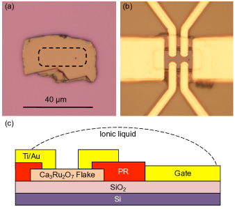
Single crystals of Ca3Ru2O7 used in this study were grown by a floating zone method. Flakes of Ca3Ru2O7 were exfoliated via mechanical cleavage from bulk crystals and deposited onto a substrate of 300 nm SiO2 thermally grown on undoped Si. Flakes are typically on the order of 30-50 m in lateral length, and between 0.5 and 1 m in thickness along the -axis; one flake is shown in Fig. 1a. Thickness was estimated by focusing the both the flake and the substrate within the sub-micron depth of view field of our optical microscope, and confirmed by atomic force microscope (AFM) measurements. We developed a process to contact only the top surface of the flake by hard-baking a photo-lithographically defined window on the surface of a flake before defining metal contacts. We patterned Ti/Au metal contacts in a Hall bar geometry. A short, low-power oxygen etch cleaned the sample surface sufficiently after processing. A completed device is shown in Fig. 1b. This surface-contacted geometry prepares the device for top-gating with an ionic liquid, shown schematically in Fig. 1c, and is preferred to maximize the surface signal in metallic, though anisotropic, materials. We use the ionic liquid N,N-diethyl-N-(2-methoxyethyl)-N-methylammonium bis(trifluoromethylsulphonyl-imide), DEME-TFSI) as the gate dielectirc. Devices were measured within a Physical Property Measurement System (Quantum Design) with a base temperature of 1.8 K and a 9T superconducting magnet. Gate voltage is applied just above the freezing point of DEME-TFSI at 210 KSato et al. (2004) and the sample is cooled with the gate voltage held constant.
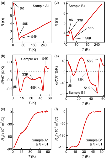
In Fig. 2, we show longitudinal resistance temperature in two Ca3Ru2O7 flake Hall bar devices. Both devices showed metallic behavior and essentially a linear behavior until an antiferromagnetic ordering transitionCao et al. (1997); Bao et al. (2008) at 54 and 56 K in these two samples, corresponding to the 56 K transition in the bulk, resulting in a sudden drop in sample resistance. Lowering temperature further, a structural transition and a sharp jump in sample resistance was found near 49 and 51 K, respectively, corresponding to the 48 K transition in the bulk Yoshida et al. (2005). However, qualitatively different behaviors were found for the two devices at low temperatures. For Sample A, the insulating behavior was found below the structure transition, persisting to around 8 K, below which a metallic behavior was found. For Sample B, the insulating behavior lived much shorter than Sample A, with a metallic behavior found below 33 K.
The temperature dependence of the sample resistance seen in Sample A is essentially that of the bulk measured along the -axis, , while that seen Sample B, resembles that of the bulk in-plane resistivity, . Kikugawa et al. (2010); Yoshida et al. (2004); Ohmichi et al. (2004) The -axis resistivity of the bulk crystals was found to feature more than a factor of eight resistance rise below the structural transition in bulk crystals, and that for our Sample A is roughly factor of 4, which suggests that the sample resistance measured in Sample A contains contributions from both - and -axis electrical transport. Interestingly, the temperature dependence of the sample resistance for Sample A, which we refer here to as a Type A sample, was found in most devices we prepared. Given that the ratio of -axis resistivity to -axis resistivity is only over factor of three, this is not unexpected. Devices with behavior resembling to that of Sample B, which we refer to as a Type B sample, were much harder to come by. The sample resistance for Type B samples consists mostly contribution from the flake surface, taking up the behavior of bulk .
The feature found at 33 K in bulk Yoshida et al. (2004), which was seen in for Sample B and in for Sample A, marks the onset of a quasi two-dimensional metallic state. The metallic behavior found in below 8 K, on the other hand, signals a incoherent-coherent transition in the -axis transport and the emergence of a fully three-dimensional metal in Ca3Ru2O7. Interestingly, the 8 K feature in was observed in floating zone,Kikugawa et al. (2010) but not in self-flux grown crystals,Yoshida et al. (2004); Ohmichi et al. (2004) which seems to suggests that coherent -axis transport is fragile, sensitive to disorder. The observation of the 8 K feature in our Type A sample therefore suggests that the good crystallinity of our flakes, consistent with the temperature dependence of the Hall coefficient, (), shown in Fig. 2c. Incidentally, small deviation from bulk behavior in () was found for Sample B at low temperatures, likely reflecting the effect of disorder on the flake surface.
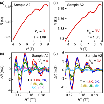
The above analysis is supported by our observation of SdHOs in Type A samples which are absent in Type B samples. We show in Fig.3a with at = 1.8 K in a Type A device. The background-subtracted resistance oscillations, , were shown in Fig. 3c. Similar behavior was found in a separate Type A device (data not shown). Up to three sets of oscillations were observed in bulk Ca3Ru2O7 .Cao et al. (2003); Kikugawa et al. (2010) However, a Fourier transform of obtained in our flake devices suggests only a single set of SdHOs with a frequency of 43 T, which was also seen in the bulk, likely due to a low maximum in the present work. It is known that the frequency of SdHOs depends on the carrier density. Even though the precise carrier density of the device cannot be obtained from the Hall measurements because the thickness of the layer affected by the gating is not known, the carriers added to the surface can be estimated based on our control experiment carried out on graphene. Careful comparison of the SdHOs without gating with those obtained when a ionic liquid gating voltage of 3 V was applied, corresponding a carrier density change larger than 1013 cm-2, the SdHOs remained essentially the same (Figs. 3c and d). This observation suggests that the SdHOs can not come from the surface of the flake. Incidentally, SdHOs were not observed in Type B samples, which, together with the deviation from the bulk behavior seen in (), indicates clearly that the transport in Type B samples is dominated by the surface layer featuring disorder stronger than that in the interior of the flake. The surface dominance in Type B samples could be due to mechanical separation formed during the exfoliation process even though there is no direct evidence for it.
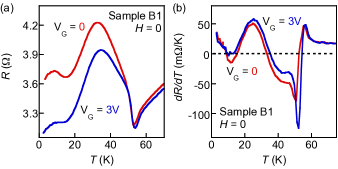
The surface layer-dominated transport in Type B samples facilitates measurable response to applied gate voltage across an ionic liquid. In Fig. 4a, we show that with = 3 V, the induction of electrons at the flake surface increases conductivity by up to 20% at lowest temperatures in the metallic regime, likely due to an added carrier density larger than 1013 cm-2 as mentioned above. In numerically calculated in Fig. 4b, we observe a shift in the peak insulating slope associated with the structural transition in Ca3Ru2O7 , from 50 to 53 K. The shift of a structural transition with carrier density confirms that the transition is electronically driven even though orbital ordering is absent. Interestingly, although recent electrical transport studies of bulk Ca3Ru2O7 under pressure have indicated that the structural transition is linked to the long-range antiferromagnetic ordering,Yoshida et al. (2008) the 56 K transition observed in our Type B sample is barely shifted (Fig. 4b).
The three-dimensional metallic state emerged below 8 K is puzzling. The area of the primary Fermi surface can be estimated from the period in of our SdHOs using the formula . A frequency of 43 T gives 0.3% of the 1st Brillouin zone, using lattice parameters from Ref. Yoshida et al. (2005), in agreement with bulk measurements of both SdHOs and ARPES.Baumberger et al. (2006) It is intriguing that the onset temperature for this metallic state with a tiny carrier density appears to be unchanged under a 3V ionic liquid gating. Together with the fact that the 56 K magnetic transition was barely shifted by the same ionic liquid gating of 3 V, our experiment seems to suggest that the emergence of this metallic phase is magnetic in origin.
In conclusion, we have developed a surface-contact technique for devices prepared on exfoliated Ca3Ru2O7 flakes. Comparison with features seen on these devices prepared on exfoliated Ca3Ru2O7 flakes and those in floating zone-grown bulk crystals suggests that the transport properties observed in the Type A and Type B samples are dominated by axis and in-plane contributions, respectively. Magneto electrical transport measurements, including the observation of SdHOs, support the emergence of a highly unusual metallic state featuring small Fermi surface pockets at low temperatures. The demonstration of an electric field effect on the structural transition temperature on Ca3Ru2O7 surface suggests a new approach to the study of complex transition metal oxides for which thin films are unavailable.
We would like to thank M. Sigrist, N. Staley and M. Ulrich for useful discussions. The work at Penn State is supported by DOE under Grant No. DE-FG02-04ER46159. The work at Tulane is supported by NSF under DMR-1205469. The nano fabrication part of this work is supported by the National Science Foundation (NSF) under Grant DMR-0908700 and Penn State MRI Nanofabrication Lab under NSF Cooperative Agreement 0335765, NNIN with Cornell University. Y. L. also acknowledges support from MOST of China (Grant 2012CB927403) and NSFC (Grant 11274229) for data analysis and manuscript preparation.
References
- Maeno et al. (1994) Y. Maeno, H. Hashimoto, K. Yoshida, S. Nishizaki, T. Fujita, J. G. Bednorz, and F. Lichtenberg, Nature 372, 532 (1994).
- Cao et al. (1997) G. Cao, S. McCall, J. E. Crow, and R. P. Guertin, Phys. Rev. Lett. 78, 1751 (1997).
- Yoshida et al. (2005) Y. Yoshida, S.-I. Ikeda, H. Matsuhata, N. Shirakawa, C. H. Lee, and S. Katano, Phys. Rev. B 72, 054412 (2005).
- Bao et al. (2008) W. Bao, Z. Q. Mao, Z. Qu, and J. W. Lynn, Phys. Rev. Lett. 100, 247203 (2008).
- McCall et al. (2003) S. McCall, G. Cao, and J. E. Crow, Phys. Rev. B 67, 094427 (2003).
- Singh and Auluck (2006) D. J. Singh and S. Auluck, Phys. Rev. Lett. 96, 097203 (2006).
- Ohmichi et al. (2004) E. Ohmichi, Y. Yoshida, S.-I. Ikeda, N. Shirakawa, and T. Osada, Phys. Rev. B 70, 104414 (2004).
- Hotta and Dagotto (2001) T. Hotta and E. Dagotto, Phys. Rev. Lett. 88, 017201 (2001).
- Forte et al. (2010) F. Forte, M. Cuoco, and C. Noce, Phys. Rev. B 82, 155104 (2010).
- Bohnenbuck et al. (2008) B. Bohnenbuck, I. Zegkinoglou, J. Strempfer, C. Schussler-Langeheine, C. S. Nelson, Ph. Leininger, H.-H. Wu, E. Schierle, J. C. Lang, G. Srajer, et al., Phys. Rev. B 77, 224412 (2008).
- Stefanovich et al. (2000) G. Stefanovich, A. Pergament, and D. Stefanovich, J. Phys.: Condens. Matter 12, 8837 (2000).
- Ruzmetov et al. (2010) D. Ruzmetov, G. Gopalakrishnan, C. Ko, V. Narayanamurti, and S. Ramanathan, J. Appl. Phys. 107, 114516 (2010).
- Tokura and Nagaosa (2000) Y. Tokura and N. Nagaosa, Science 288, 462 (2000).
- Kikugawa et al. (2010) N. Kikugawa, A. W. Rost, C. W. Hicks, A. J. Schofield, and A. P. Mackenzie, J. Phys. Soc. Jpn. 79, 024704 (2010).
- Novoselov et al. (2005) K. S. Novoselov, D. Jiang, F. Schedin, T. J. Booth, V. V. Khotkevich, S. V. Morozov, and A. K. Geim, PNAS 102, 10451 (2005).
- Yoshida et al. (2007) Y. Yoshida, S.-I. Ikeda, and N. Shirakawa, J. Phys. Soc. Jpn. 76, 085002 (2007).
- Yuan et al. (2009) H. Yuan, H. Shimotani, A. Tsukazaki, A. Ohtomo, M. Kawasaki, and Y. Iwasa, Adv. Funct. Mater. 19, 1046 (2009).
- Skinner et al. (2010) B. Skinner, M. S. Loth, and B. I. Shklovskii, Phys. Rev. Lett. 104, 128302 (2010).
- Ueno et al. (2011) K. Ueno, S. Nakamura, H. Shimotani, H. T. Yuan, N. Kimura, T. Nojima, H. Aoki, Y. Iwasa, and M. Kawasaki, Nat. Nanotechnol. 6, 408 (2011).
- Leng et al. (2011) X. Leng, J. Garcia-Barriocanal, S. Bose, Y. Lee, and A. M. Goldman, Phys. Rev. Lett. 107, 027001 (2011).
- Yamada et al. (2011) Y. Yamada, K. Ueno, T. Fukumura, H. T. Yuan, H. Shimotani, Y. Iwasa, L. Gu, S. Tsukimoto, Y. Ikuhara, and M. Kawasaki, Science 332, 1065 (2011).
- Sato et al. (2004) T. Sato, G. Masuda, and K. Takagi, Electrochim. Acta 49, 3603 (2004).
- Yoshida et al. (2004) Y. Yoshida, I. Nagai, S.-I. Ikeda, N. Shirakawa, M. Kosaka, and N. Mori, Phys. Rev. B 69, 220411(R) (2004).
- Cao et al. (2003) G. Cao, L. Balicas, Y. Xin, J. E. Crow, and C. S. Nelson, Phys. Rev. B 67, 184405 (2003).
- Yoshida et al. (2008) Y. Yoshida, M. Hedo, S.-I. Ikeda, N. Shirakawa, and Y. Uwatoko, Physica B 403, 1213 (2008).
- Baumberger et al. (2006) F. Baumberger, N. J. C. Ingle, N. Kikugawa, M. A. Hossain, W. Meevasana, R. S. Perry, K. M. Shen, D. H. Lu, A. Damascelli, A. Rost, et al., Phys. Rev. Lett. 96, 107601 (2006).