Double injection, resonant-tunneling recombination, and current-voltage characteristics in double-graphene-layer structures
Abstract
We evaluate the effect of the recombination associated with interlayer transitions in ungated and gated double-graphene-layer (GL) structures on the injection of electrons and holes. Using the proposed model, we derive analytical expressions for the spatial distributions of the electron and hole Fermi energies and the energy gap between the Dirac points in GLs as well as their dependences on the bias and gate voltages. The current-voltage characteristics are calculated as well. The model is based on hydrodynamic equations for the electron and hole transport in GLs under the self-consistent electric field. It is shown that in undoped double-GL structures with weak scattering of electrons and holes on disorder, the Fermi energies and the energy gap are virtually constant across the main portions of GLs, although their values strongly depend on the voltages and recombination parameters. In contrast, the electron and hole scattering on disorder lead to substantial nonuniformities. The resonant inter-GL tunneling enables N-shaped current-voltage characteristics provided that GLs are sufficiently short. The width of the current maxima is much larger than the broadening of the tunneling resonance. In the double-GL structures with relatively long GLs the N-shaped characteristics transform into the Z-shaped characteristics. The obtained results are in line with the experimental observations 1 and might be useful for design and optimization of different devices based on double-GL structures, including field-effect transistors and terahertz lasers.
I Introduction
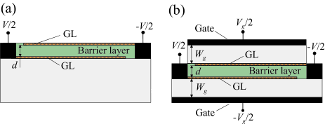
Double-graphene-layer (double-GL) structures, which consist of two GLs separated by a thin layer and independently connected with the side contacts, were fabricated and studied recently 1 ; 2 ; 3 ; 4 . Such structures have drawn a considerable attention. This, in part, is due to potential applications of the double-GL structures in optically transparent transistor circuits 1 ; 2 ; 3 , high speed modulators of optical and terahertz (THz) radiation 3 ; 4 ; 5 ; 6 , THz detectors and frequency multipliers 7 ; 8 ; 9 , THz photomixers 10 , and THz lasers 11 . Schematic views of the double-GL structures (both ungated and gated) and their band diagram under the bias voltage are shown in Fig.1. Interesting features of devices based on independently contacted quantum wells, formed in the standard heterostructures, were discussed some time ago 12 . Under the operation conditions of different double-GL-based devices, the inter-GL transitions (tunneling or thermionic) tend to depopulate GLs. This can lead to a disruption of the device operation. The refilling of GLs is associated with the injection of electrons to one GL and holes another from the pertinent contacts. Thus, the injection of electrons and holes in the double-GL structures requires a careful consideration. In this paper, we develop a model for transport phenomena in the double-GL structures shown ind Fig. 1(a) and 1(b) employing the hydrodynamic equations coupled with the Poisson equation for the self-consistent electric potential 13 ; 14 . Similar problem, but related to single- and multiple-GL structures with injection of both electrons and holes into the same GL from the opposite n- and p-contacts, was considered recently 13 ; 14 . However, the double-GL structures with independently contacted GLs are characterized by important features associated with spatial separation of interacting two-dimensional electron Gas (2DEG) and two-dimensional holes gas (2DHG). In particular, the existence of the energy gap between the Dirac points in GLs and the resonant tunneling between GLs should be addressed.
The paper is organized as follows. In Sec. II, we discuss the device model and write down the main equations which govern the transport and recombination of the injected electrons in the main parts GLs, where the latter are quasi-neutral. The role of the near-contact regions is accounted by the boundary condition set at the edges of the quasi-neutral regions 14 . Section III deals with the calculations of the spatial distributions and voltage dependences of the Fermi energy, the energy gap, and electric potential assuming that the electron-hole scattering dominates over the scattering on disorder. In Sec. IV, we found how the disorder scattering affects the spatial distributions and voltage dependences. In Sec. V, the current-voltage characteristics are calculated and discussed using the results of Sec. IV. In Sec. VI, we draw the main conclusions.
II Model and the pertinent equations
We assume that GLs in the double-GL structures under consideration are ungated and undoped [see Fig. 1(a)], or gated and ”electrically” doped. In the latter case, GLs are filled with 2DEG and 2DHG [see Fig. 1(b)] electrically induced by the gate voltages . The application of the bias voltage between the opposite edges of the ungated GLs [as shown in Fig. 1(a)] results in the formation of 2DEG and 2DHG in the pertinent GLs. In the gated double-GL structure shown in Fig. 1(b), the 2DEG and 2DHG densities are determined by both the bias and gate voltages, and . The double-GL structures under consideration are particularly interesting for devices utilizing the resonant tunneling between GLs and resonant tunneling assisted by the photon emission 11
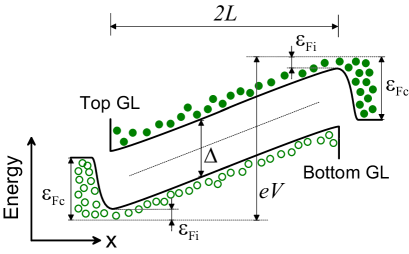
As shown previously by numerical solutions of the two-dimensional Poisson equation with realistic boundary conditions and structural parameters 14 , in sufficiently long GL- structures (their length significantly exceeds the characteristic screening length , i.e., the parameter , in the main part of GLs the electron-hole plasma is quasi-neutral. Here is the temperature (in the energy units), cm/s is the characteristic velocity of electrons and holes in GLs, is the dielectric constant, and is the Planck constants. Indeed, if and m at the temperatures K, parameter . Thus the electron density in one GL,, is with high accuracy equal to the hole density in another GL: . Figure 2 schematically shows the Dirac points spatial positions (separated by the energy gap ) and potential profiles in both GLs under the applied bias voltage . This figure demonstrates qualitatively that the potential profiles being rather sharp near the contact regions are smooth in the main parts of GLs.
At sufficiently high bias and gate voltages, the 2DEG and 2DHG density are large, so that the electron and hole energy distributions are well characterized by the Fermi functions with the quasi-Fermi energies (counted from the Dirac points) and the common effective temperature . The latter is assumed to be equal to the lattice temperature.
The electron and hole density in the pertinent GLs and the energy gap between the Dirac points are related to each other as is
| (1) |
where is the density of 2DEG and 2DHG induced by the gate voltages , is the spacing between GLs and is the spacing between the GLs and gates [see Figs. 1(a) and 1(b)] Generally , the energy gap , i.e., the energy separation between the Dirac points in GLs, (which determines the built-in electric field in the inter-GL barrier), as well as and the electric potential at the GL plane are functions of coordinate (the -axis is directed in the Gl plane from the p- to n-contacts).
In the case of the 2DEG and 2DHG strong degeneration () ,
| (2) |
| (3) |
where .
In the absence of the inter-GL recombination, 2DEG and 2DHG are in equilibrium. In this case, Fermi energy in each GL and the energy gap are given by
| (4) |
| (5) |
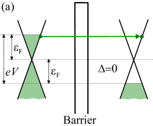
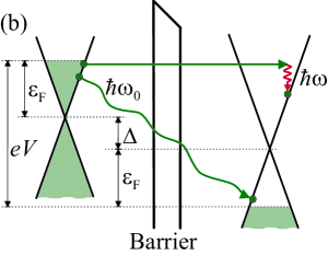
where and . At , , but at , . In particular, when , i.e., , at all . Figure 3 shows the energy diagrams of a double-GL structure at and .
High densities of 2DEG and 2DHG assume the validity of a hydrodynamic approach for the description of the electron and hole transport. We use the hydrodynamic model presented in Ref. 14 .
The transport of electrons and holes is governed by the following system of hydrodynamic equations 14 :
| (6) |
| (7) |
| (8) |
| (9) |
Here and are the value of the electron and hole hydrodynamic velocities and and are the potentials of the top GL (filled with electrons) and the bottom GL (filled with holes), respectively, is the collision frequency of electrons and holes with impurities and acoustic phonons (with the short-range disorder), is their collision frequency with each other, is the fictitious mass, which at the Fermi energies of the same order of magnitude as the temperature can be considered as a constant, and .
The recombination of the major carriers injected to the degenerate 2DEG and 2DHG in the double-GL structures under consideration is primarily associated with the inter-GL transitions. The rate of these processes depends of the Fermi energy (density of 2DEG and 2DHG) and the energy gap . When , the resonant-tunneling transitions with the conservation of momentum can dominate 1 ; 7 ; 15 ; 16 . Such transitions correspond to the arrow in Fig. 3(a). We present the rate of the resonant-tunneling recombination in the following form:
| (10) |
where is the characteristic resonant-tunneling recombination time and is the resonance broadening parameter.
The inter-GL transitions due to the scattering on impurities or acoustic phonons (non-resonant processes) and due to the processes mediated by photons see Fig. 3(b)] in which the momentum or energy are not conserved can also contribute to the recombination. Due to a strong coupling of electrons and holes with optical phonons, the processes assisted by optical phonon emission can also greatly contribute to the rate of the inter-GL transitions (as it takes place in GL structures with bipolar injection into GLs 10 ; 14 ; 17 ; 18 ; 19 ). For concreteness, we assume that the resonant-tunneling processes and the processes accompanied by oprical phonon emission are the main mechanisms of the inter-GL recombination.
In the case mV, , and the transitions between the tails of the energy distributions are possible. At meV, the inter-GL transitions assisted by the optical phonon emission are not limited by the Pauli exclusion principle [see Fig. 3(b)]. In this case, the inter-GL recombination can be rather strong restricting penetration of the injected electrons and hole sufficiently far from GL edges. Considering this, the rate of the nonresonant inter-GL recombination assisted by optical phonon emission can be presented as
| (11) |
if , and
| (12) |
if Here is the characteristic recombination time associated with and with the inter-GL transitions assisted by the optical phonon emission, respectively, is the rate thermogeneration of the electron-hole pairs due to the absorption of optical phonons in equilibrium (it is about cm-2s-1 at room temperature 16 ), and is the tunneling decay factor characterizing the overlap of wavefunctions in the top and bottom GLs, The right-hand side of Eq. (11), which provides a somewhat simplified dependence of the recombination rate on and , which differs from that used in Ref. 14 ; 15 (see also Refs. 16 ; 17 ) for the recombination rate associated with the intra-GL transitions mediated by optical phonons by factors and . The latter is due to the energy gap associated with the GL spatial separation and the potential difference between GLs. Invoking Ref. 17 , we find s. Hence, accounting for that , one obtains s. According to the experimental results 1 , the rate of the inter-GL transitions at the resonant tunneling cm-2s-1. This yields s-1.
Thus, the net inter-GL recombination rate is assumed to be as
| (13) |
Considering the same boundary conditions as in Ref. 14 set at the points near the contacts (outside narrow space-charge regions) i.e., at , but generalized by accounting for the energy gap (see Fig. 2), we have
| (14) |
.
The boundary conditions for the electron and hole velocities can be taken as (no electron and hole current at the disconnected GL edges)
| (15) |
.
As in Ref. 14 , we introduce the following dimensionless variables: , , , , , , , , and . In these notations, the dimensionless generation-recombination term and the dimensionless density are
| (16) |
| (17) |
| (18) |
| (19) |
| (20) |
where , where the function is numerically calculated in Appendix, , , and . The parameter varies in a wide range depending on on the scattering and recombination parameters and the GL length.
The quantity can be presented as , where is the diffusion length and is the bipolar diffusion coefficient.
III Spatial and voltage dependences of Fermi Energy, energy gap, and potential
In the structures under consideration in which the density of 2DEG and 2DHG markedly exceeds the density residual impurities, one can assume that (even despite the spatial separation of 2DEG and 2DHG). Taking this into account, we disregard in Eqs. (10) and (11) the terms proportional to a small parameter . In such a case, Eqs. (16) - (18), with boundary conditions which follow from Eqs. (14) and (15), yield , , , and , where :
| (21) |
| (22) |
| (23) |
As follows from the boundary conditions, and are related to each other also as:
| (24) |
Considering Eqs. (22) and (23), we arrive at the following equation for :
| (25) |
The quantity in Eq. (23), which is proportional to , explicitly describes the effect of spatial separation of GLs resulting in the appearance of the energy gap. According to the above formulas, the Fermi energy and the energy gap are independent of the coordinate (in the main parts of GLs except near-contact regions), while potential is a linear function of the coordinate see Eq. (22)]. This corresponds to Fig. 2.
If the inter-GL recombination is insignificant, formally setting , from Eq. (24), we obtain the equilibrium value of the Fermi energy in each GL, and, hence, using Eq. (23), the equilibrium value of the energy gap coinciding with Eqs. (4) and (5).
Equation (25) yields the explicit relationship between the normalized Fermi energy in the main portions of GLs (excepts narrow regions near the contacts) on parameters and , the bias voltage , and the gate voltage [via the dependence ]. At relatively weak electron-hole scattering (and the scattering on disorder)and recombination when and 2DEG and 2DHG are close to equilibrium, Eqs. (23) - (25) yield and close to and [see Eqs. (4) and (5)].
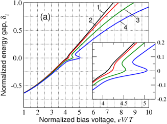
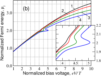
Figure 4 shows the dependences of the normalized energy gap and the normalized Fermi energy, in the main parts of GLs calculated using Eqs. (23) - (25) for the parameter in the range of (). It was assumed that , nm, , K, and (i.e., mV), so that . meV, . We used the functions (for ) and calculated in Appendix.
Using the data obtained from Ref. 1 ( s and m2), one can find . The quantity corresponds to s (see Sec. II). As seen from Fig. 4, at relatively small values of parameter both and increase monotonically with increasing the bias voltage (see curves 1 and 2). At elevated values of parameter , for example at relatively long GLs (see curves 3 and 4), the voltage dependences of and are of the S-shape, i.e., multi-valued in a certain voltage range corresponding to the tunneling resonance ). The monotonic and multi-valued behavior correspond, in particular, to relatively short and long GLs, respectively ()
IV Role of scattering on disorder
Although the scattering of electrons and holes on residual impurities and acoustic phonons is comparably weak, it can lead to a small but qualitative modification of the injection characteristics. Considering the terms with as perturbations, one can search for solutions of Eqs. (15) - (18) in the form: , , and so on. In particular, we arrive at the following equation for the variation of the Fermi energy:
| (26) |
Taking into account that , from Eq. (26) we obtain
| (27) |
Here . Simultaneously, one can find
| (28) |
As follows from Eqs. (27) and (28), the scattering of electrons and holes on disorder results in the spatial distributions of the Fermi energy (i.e., ) and the energy gap with minima at the center of the structure (). The span of these quantities variations are as follows:
| (29) |
| (30) |
where we have introduced the diffusion lengths associated with the scattering on disorder.
V Current-voltage characteristics
The inter-GL current is calculated using the expression for the rate of the pertinent transitions as a function of the local values of the Fermi energy integrated over the GL length:
| (31) |
Here
| (32) |
is the width of GLs (in the direction perpendicular to the current), and is given by Eq. (20). If , so that in the main parts of GLs, Eq. (31) can be rewritten as
| (33) |
At the tunneling resonance at which and , the current is equal to (if , i.e., )
| (34) |
if , and
| (35) |
if . When , i.e., mV, , and , Eq. (34) yields . At higher values of , the voltage dependence of the current peak height tends to saturation or becomes relatively slow if a relatively weak (non-exponential) dependence on the non-resonant inter-GL transition rate is accounted for .
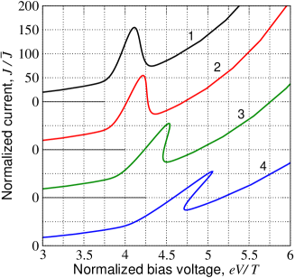
Figure 5 shows the current-voltage characteristics calculated using Eq. (30) with Eqs. (20), (23), and (25) for the same parameters as in Fig. 4. As seen from Fig. 5, the current-voltage characteristics exhibit pronounced maxima corresponding to the tunneling resonances. Indeed, the bias voltage at which the current reaches the maximum coincide with that corresponding to [see Fig. 4(a)]. It should be noted that the width, , of the maxima markedly exceeds the width, mV, of the resonant maximum of the inter-GL transition rate by the order of magnitude. However, the most remarkable feature of the obtained current-voltage characteristics is the transformation of their shape from the N-type (curves 1 and 2) to the Z-type (curves 3 and 4) when the parameter increases. As seen from Fig. 5, the current-voltage characteristics become multi-valued (when the voltage dependences of the Fermi energy and the energy gap become of the S-shape) in certain voltage ranges if the parameter is sufficiently large (i.e., if the length of GL is relatively large). The effect of broadening of the resonant maxima in the current-voltage characteristics is due to relatively slow variations of the energy gap with varying bias voltage. Indeed, the width of the current-voltage resonant peak can be estimated as . Since [see Fig. 4(a)], . Even at , when 2DEG and 2DHG in the pertinent GLs are close to equilibrium, for the parameters used in the above calculations. An increase in results in further decreasing of and, hence, increasing the width of the current-voltage resonant peak. The occurrence of the voltage range where they are multi-valued, i.e., the transformation of the N-shaped current-voltage characteristics to the Z-shaped ones can be attributed to the potential drop across GLs. Similar effect in quantum-well resonant-tunneling transistors and other tunneling devices was considered previously 21 ; 22 ; 23 ; 24 ; 25 (see also Ref. 26 ). For the values s-1 and s-1 used above and m2 (as in Ref. 1 ), the tunneling resonant peak current () is in the range nA, i.e., of the same order of magnitude as in the experiment 1 .
An increase in the gate voltage leads to an increase in the Fermi energy (i.e., ) and, hence, to an increase in (i.e., ). As a result, the position of the current peak shifts to higher bias voltages.
The shift of the current maxima associated with an increase in and, consequently, occurs when the levels of the chemical doping of GLs are elevated (the donor density in the top GL and the acceptor density in the bottom GL increase). In this case, the resonant condition is achieved at higher bias voltage . Just such doped structures were studied in Ref. 1 , in which the current peaks correspond to higher values of the bias voltages ( about several tenth of Volt) than in Fig. 5 ( V) for the chemically undoped GLs. However, an increase in the dopant densities leads to an increase in the collision frequency . This can result in a marked effect of the disorder scattering to the spatial distributions of the Fermi energy, the energy gap [see Eqs. (27) and (28)], and the current. Due to this, the function in Eq. (31) becomes coordinate-dependent. This leads to lowering of the current peak and its additional broadening (inhomogenious). Indeed, using Eqs. (27) and (31) at (when and integrating over , we obtain
| (36) |
where . Since is negative, from Eq. (33) we obtain with
Taking into account that at (where is independent of a and , Eq. (35) can be presented as
| (37) |
The latter quantity is proportional to a small factor and two large factors and . Hence even relatively weak scattering on disorder can markedly affect the shape of the maxima in the current-voltage characteristics.
VI Conclusions
In conclusion:
(1) We have developed the device model for the double-GL structures with independently contacted GLs which describes the processes of the electron and hole injection from the opposite contacts accompanied with the inter-GL electron-hole recombination.
(2) Using the model, we have derived analytical expressions for the spatial distributions of the electron and hole Fermi energies and the energy gap between the Dirac points in GLs as functions of the bias and gate voltages and the structural parameters. It has been shown that these quantities can be virtually coordinate-independent in the main parts of GLs (except narrow near contact regions) if the mutual scattering of electrons and holes dominate. An increase in relative strength of electron and hole scattering on disorder can lead to substantial sag of the spatial dependences in question with the minima in the center of the GL structures. The shape of the Fermi energy versus voltage characteristics varies from the monotonic to the S-type with increasing length of GLs.
(3) We have calculated the current-voltage characteristics and revealed that they exhibit maxima associated with the resonant-tunneling inter-GL transitions (the N-type characteristics) in the GL-structures with relatively short GLs. In the structures with long GLs, the N-type characteristics can transform to the Z-type characteristics. In the latter case, the effect of hysteresis can exist. This should be taken into account choosing the range of operation voltages of the lasers based on the double-GL structures 11 ; 27 .
(4) The obtained results are in line with recent experimental observations 1 . They can be useful for the development and optimization of double-GL-based field-effect transistors, terahertz detectors, and terahertz lasers.
Acknowledgments
The authors are grateful to A. Satou and D. Svintsov for useful discussions. This work was supported by the Japan Society for Promotion of Science (Grant-in-Aid for Specially Promoting Research), Japan. The work at UB was supported by the NSF-TERANO Program.
Appendix

.
The function is given by Eq. (19). At , , while at large , one obtains . The function , where according to Ref. 13 (see, also, Ref. 20 ) and considering the Thomas-Fermi screening of the electron-hole interaction,
| (A1) |
where and (at , ). Figure 6 shows and calculated numerically using Eqs. (16) and (A1), respectively.
References
- (1) L. Britnell, R. V. Gorbachev, A. K. Geim, L. A. Ponomarenko, A. Mishchenko, M. T. Greenaway, T. M. Fromhold, K. S. Novoselov, and L. Eaves, Nature Comm. 4, 1794-1799 (2013).
- (2) L. Britnell, R. V. Gorbachev, R. Jalil, B. D. Belle, F. Shedin, A. Mishenko, T. Georgiou, M. I. Katsnelson, L. Eaves, S. V. Morozov, N. M. R. Peres, J. Leist, A. K. Geim, K. S. Novoselov, and L. A. Ponomarenko, Science, 335, 947 (2012).
- (3) T. Georgiou, R. Jalil, B. D. Bellee, L. Britnell, R. V. Gorbachev, S. V. Morozov, Y.-J. Kim, A. Cholinia, S. J. Haigh, O. Makarovsky, L. Eaves, L. A. Ponomarenko, A. K. Geim, K. S. Novoselov, and A. Mishchenko, Nature Nanotechnology 7, 100 (2013).
- (4) M. Liu, X. Yin, and X. Zhang, Nano Lett. 12,1482-1485 (2012).
- (5) V. Ryzhii, T. Otsuji, M. Ryzhii, V. G. Leiman, S. O. Yurchenko, V. Mitin, and M. S. Shur, J. Appl. Phys. 112, 104507 (2012).
- (6) S. Svintsov, V. Vyurkov, V. Ryzhii, and T. Otsuji, J. Appl. Phys. 111, 083715 (2012).
- (7) P. Zhao, R. M. Feenstra, G. Gu, and D. Jena, IEEE Trans. Electron Devices, 60, 951 (2013).
- (8) V. Ryzhii, T. Otsuji, M. Ryzhii, and M. S. Shur, J. Phys. D: Appl. Phys. 45, 302001 (2012).
- (9) V. Ryzhii, A. Satou, T. Otsuji, M. Ryzhii, V. Mitin, and M. S. Shur, J. Phys. D: Appl. Phys. 46 (2013) 315107.
- (10) V. Ryzhii, M. Ryzhii, V. Mitin, M. S. Shur, A. Satou, and T. Otsuji, J. Appl. Phys. 113, 174506 (2013).
- (11) V. Ryzhii, A. A. Dubinov, V. Ya. Aleshkin, M. Ryzhii, and T. Otsuji, Appl. Phys. Lett. 103, 163507 (2013).
- (12) Z. S. Gribnikov, A. N. Korshak, and V. V. Mitin, J. Appl. phys. 83, 1481 (1998).
- (13) D. Svintsov, V. Vyurkov, S. Yurchenko, T. Otsuji, and V. Ryzhii, J. Appl. Phys. 111, 083715 (2012).
- (14) V. Ryzhii, I. Semenikhin, M. Ryzhii, D. Svintsov, V. Vyurkov, A. Satou, and T. Otsuji, J. Appl. Phys., 113, 244505 (2013).
- (15) R. M. Feenstra, D. Jena, and G. Gu, J. Appl. Phys. 111, 043711 (2012).
- (16) F. T. Vasko, Phys. Rev. B 87, 075424 (2013).
- (17) F. Rana, P. A. George, J. H. Strait, S. Shivaraman, M. Chandrashekhar, and M. G. Spever, Phys. Rev. B 79, 115447 (2009).
- (18) V.Ryzhii, M. Ryzhii, V. Mitin, and T. Otsuji, J. Appl. Phys. 110, 094503 (2011).
- (19) V. Ryzhii, M. Ryzhii A. Satou, T. Otsuji, A. A. Dubinov, and V. Ya. Aleshkin, J. Appl. Phys. 107, 054505 (2009).
- (20) A. Kashuba, Phys. Rev. B 78, 085415 (2008).
- (21) V. Ryzhii, O. Kosatykh, B. Tolstikhin and I. Khmyrova, Sov. Microelectron. 18, 84 (1989).
- (22) V. Ryzhii and I. Khmyrova, Sov. Phys. Semicond. 25, 387 (1991).
- (23) B. A. Glavin, V. A. Kochelap, and V. V. Mitin, Phys. Rev. B 56, 13346 (1997).
- (24) M. Meixner, P. Rodin, E. Scholl, and A. Wacker, Eur. Phys. B 13, 157 (2000).
- (25) O. V. Pupysheva, A. V. Dmitriev, A. A. Farajuan, H. Mizuseki, and Y. Kawazoe, J. Appl. Phys. 100, 033716 (2006).
- (26) A. Wacker and E. Scholl, J. Appl. Phys. 78, 7352 (1995).
- (27) V. Ryzhii, A. A. Dubinov, T. Otsuji, V. Ya. Aleshkin, M. Ryzhii, and M. S. Shur, Optics Express 21, 31560 (2013).