Magneto-transport characteristics of a 2D electron system driven to negative magneto-conductivity by microwave photoexcitation
Abstract
Negative diagonal magneto-conductivity/resistivity is a spectacular- and thought provoking- property of driven, far-from-equilibrium, low dimensional electronic systems. The physical response of this exotic electronic state is not yet fully understood since it is rarely encountered in experiment. The microwave-radiation-induced zero-resistance state in the high mobility GaAs/AlGaAs 2D electron system is believed to be an example where negative magneto-conductivity/resistivity is responsible for the observed phenomena. Here, we examine the magneto-transport characteristics of this negative conductivity/resistivity state in the microwave photo-excited two-dimensional electron system (2DES) through a numerical solution of the associated boundary value problem. The results suggest, surprisingly, that a bare negative diagonal conductivity/resistivity state in the 2DES under photo-excitation should yield a positive diagonal resistance with a concomitant sign reversal in the Hall voltage.
Negative magneto-conductivity/resistivity is a spectacular- and thought provoking- theoretical property of microwave photoexcited, far-from-equilibrium, two-dimensional electronic systems. This property has been utilized to understand the experimental observation of the microwave-radiation-induced zero-resistance states in the GaAs/AlGaAs system.grid1 ; grid2 Yet, the negative conductivity/resistivity state remains an enigmatic and open topic for investigation, although, over the past decade, photo-excited transport has been the subject of a broad and intense experimental grid1 ; grid2 ; grid3 ; grid4 ; grid201 ; grid202 ; grid5 ; grid6 ; grid7 ; grid8 ; grid9 ; grid11 ; grid209 ; grid203 ; grid12 ; grid13 ; grid15 ; grid16 ; grid17 ; grid19 ; grid20 ; grid16b ; grid204 ; grid21z ; grid21b ; grid104 ; grid21 ; grid21y ; grid22 ; grid60 ; grid61 ; grid22z ; grid22a ; grid22c ; grid108 ; grid109 and theoreticalgrid23 ; grid24 ; grid25 ; grid101 ; grid27 ; grid28 ; grid29 ; grid30 ; grid111 ; grid31 ; grid32 ; grid33 ; grid34 ; grid35 ; grid37 ; grid206 ; grid39 ; grid40 ; grid42 ; grid43 ; grid44 ; grid45 ; grid46 ; grid47 ; grid49 ; grid112 ; grid62 ; grid63 ; grid107 ; grid103 study in the 2D electron system (2DES).
In experiment, the microwave-induced zero-resistance states arise from ”1/4-cycle-shifted” microwave radiation-induced magnetoresistance oscillations in the high mobility GaAs/AlGaAs systemgrid1 ; grid4 ; grid22a as these oscillations become larger in amplitude with the reduction of the temperature, , at a fixed microwave intensity. At sufficiently low under optimal microwave intensity, the amplitude of the microwave-induced magnetoresistance oscillations becomes large enough that the deepest oscillatory minima approach zero-resistance. Further reduction in then leads to the saturation of the resistance at zero, leading to the zero-resistance states that empirically look similar to the zero-resistance states observed under quantized Hall effect conditions.grid1 ; grid2 ; grid5 Similar to the situation in the quantized Hall effect, these radiation-induced zero resistance states exhibit activated transport.grid1 ; grid2 ; grid5 ; grid8 A difference with respect to the quantized Hall situation, however, is that the Hall resistance, , does not exhibit plateaus or quantization in this instance where the zero-resistance state is obtained by photo-excitation.grid1 ; grid2 ; grid5
Some theories have utilized a two step approach to explain the microwave-radiation-induced zero-resistance states. In the first step, theory identifies a mechanism that helps to realize oscillations in the diagonal magneto-photo-conductivity/resistivity, and provides for the possibility that the minima of the oscillatory diagonal conductivity/resistivity can even take on negative values.grid23 ; grid25 ; grid27 ; grid111 ; grid46 ; grid33 The next step in the two step approach invokes the theory of Andreev et al.,grid24 who suggest that the zero-current-state at negative resistivity (and conductivity) is unstable, and that this favors the appearance of current domains with a non-vanishing current density,grid24 ; grid43 followed by the experimentally observed zero-resistance states.
There exist alternate approaches which directly realize zero-resistance states without a de-tour through negative conductivity/resistivity states. Such theories include the radiation-driven electron-orbit- model,grid34 the radiation-induced-contact-carrier-accumulation/depletion model,grid112 and the synchronization model.grid103 Thus far, however, experiment has been unable to clarify the underlying mechanism(s), so far as the zero-resistance states are concerned.
The negative magneto-conductivity/resistivity state suggested theoretically in this problemgrid23 ; grid25 ; grid27 ; grid111 ; grid46 ; grid33 has been a puzzle for experiment since it had not been encountered before in magneto-transport. Naively, one believes that negative magneto-resistivity/conductivity should lead to observable negative magneto-resistance/conductance, based on expectations for the zero-magnetic-field situation. At the same time, one feels that the existence of the magnetic field is an important additional feature, and this raises several questions: Could the existence of the magnetic field be sufficiently significant to overcome nominal expectations, based on the zero-magnetic-field analogy, for an instability in a negative magneto-conductivity/resistivity state? If an instability does occur for the negative magneto-conductivity/resistivity state, what is the reason for the instability? Could negative conductivity/resistivity lead to observable negative conductance/resistance at least in some short time-scale transient situation where current domains have not yet formed? Indeed, one might ask: what are the magneto-transport characteristics of a bare negative conductivity/resistivity state? Remarkably, it turns out that an answer has not yet been formulated for this last question.
To address this last question, we examine here the transport characteristics of the photo-excited 2DES at negative diagonal conductivity/resistivity through a numerical solution of the associated boundary value problem. The results suggest, rather surprisingly, that negative conductivity/resistivity in the 2DES under photo-excitation should generally yield a positive diagonal resistance, i.e., , except at singular points where when the diagonal conductivity . The simulations also identify an associated, unexpected sign reversal in the Hall voltage under these conditions. These features suggest that nominal expectations, based on the zero-magnetic-field analogy, for a negative conductivity/resistivity state in a non-zero magnetic field, need not necessarily follow, and that experimental observations of zero-resistance and a linear Hall effect in the photo-excited GaAs/AlGaAs system could be signatures of vanishing conductivity/resistivity.
I Results
I.1 Experiment
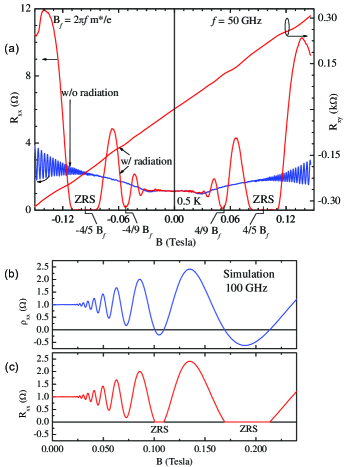
Figure 1(a) exhibits measurements of and over the magnetic field span Tesla at . The blue curve, which exhibits Shubnikov-de Haas oscillations at Tesla, represents the in the absence of photo-excitation (w/o radiation). Microwave photo-excitation of this GaAs/AlGaAs specimen at GHz, see red traces in Fig. 1, produces radiation-induced magnetoresistance oscillations in , and these oscillations grow in amplitude with increasing . At the deepest minimum, near , where ,grid1 the saturates at zero-resistance. Note also the close approach to zero-resistance near . Although exhibits zero-resistance, the Hall resistance exhibits a linear variation over the -span of the zero-resistance states, see Fig. 1(a).grid1 ; grid2
I.2 Negative magneto-resistivity and zero-resistance
Both the displacement theory for the radiation-induced magnetoresistivity oscillations,grid23 and the inelastic model,grid33 suggest that the magnetoresistivity can take on negative values over the -spans where experiment indicates zero-resistance states. For illustrative purposes, such theoretical expectations for negative resistivity are sketched in Fig. 1(b), which presents the simulated at GHz. This curve was obtained on the basis of extrapolating, without placing a lower bound, the results of fits,grid202 which have suggested that the radiation-induced oscillatory magnetoresistivity, , where , with the device width-to-length ratio, follows . Here, , with GHz, the microwave frequency, , the effective mass, , the electron charge, and , with the dark resistivity which reflects typical material characteristics for the high mobility GaAs/AlGaAs 2DES. This figure shows that the deepest minima at Tesla and Tesla exhibit negative resistivity, similar to theoretical predictions.grid23 ; grid25 ; grid27 ; grid111 ; grid46 ; grid33
Andreev et al.grid24 have reasoned that the only time-independent state of a system with negative resistivity/conductivity is characterized by a current which almost everywhere has a magnitude fixed by the condition that nonlinear dissipative resistivity equals zero. This prediction implies that the curve of Fig. 1(b) is transformed into the magnetoresistance, , trace shown in Fig. 1(c), where the striking feature is the zero-resistance over the -domains that exhibited negative resistivity in Fig. 1(b). The curve of Fig. 1(c) follows from Fig. 1(b) upon multiplying the ordinate by the ratio, i.e., , and placing a lower bound of zero on the resulting .
I.3 Device configuration
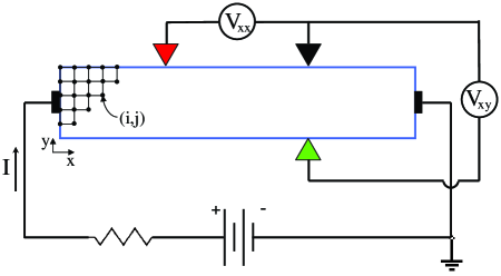
As mentioned, a question of interest is: what are the transport characteristics of a bare negative magneto-conductivity/resistivity state? To address this issue, we reexamine the experimental measurement configuration in Fig. 2. Transport measurements are often carried out in the Hall bar geometry which includes finite size current contacts at the ends of the device. Here, a constant current is injected via the ends of the device, and ”voltmeters” measure the diagonal () and Hall () voltages between probe points as a function of a transverse magnetic field, as indicated in Fig. 2. Operationally, the resistances relate to the measured voltages by and .
I.4 Simulations
Hall effect devices can be numerically simulated on a grid/mesh,grid99 ; grid110 ; grid102 see Fig. 2, by solving the boundary value problem corresponding to enforcing the local requirement , where is the 2D current density with components and , , and is the conductivity tensor.grid99 ; grid110 Enforcing within the homogeneous device is equivalent to solving the Laplace equation , which may be carried out in finite difference form using a relaxation method, subject to the boundary conditions that current injected via current contacts is confined to flow within the conductor. That is, current perpendicular to edges must vanish everywhere along the boundary except at the current contacts. We have carried out simulations using a point grid with current contacts at the ends that were 6 points wide. For the sake of simplicity, the negative current contact is set to ground potential, i.e., , while the positive current contact is set to . In the actual Hall bar device used in experiment, the potential at the positive current contact will vary with the magnetic field but one can always normalize this value to 1 to compare with these simulations.
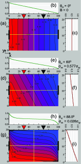
Figure 3 summarizes the potential profile within the Hall device at three values of the Hall angle, . Fig. 3(a) shows a color plot of the potential profile with equipotential contours within the device at , which corresponds to the situation. This panel, in conjunction with Fig. 3(b), shows that the potential drops uniformly within the device from the left- to the right- ends of the Hall bar. Fig. 3(c) shows the absence of a potential difference between the top- and bottom- edges along the indicated yellow line at . This feature indicates that there is no Hall effect in this device at , as expected.
Figure 3(d) shows the potential profile at , which corresponds to the situation where . Note that, here, the equipotential contours develop a tilt with respect to the same in Fig. 3(a). Fig. 3(e) shows a mostly uniform potential drop from the left to the right edge along the line at , as Fig. 3(f) shows a decrease in the potential from the bottom to the top edge. This potential difference represents the Hall voltage under these conditions.
Figure 3(g) shows the potential profile at , which corresponds to the situation where . Note that in the interior of the device, the equipotential contours are nearly parallel to the long axis of the Hall bar, in sharp contrast to Fig. 3(a). Fig. 3(h) shows the potential variation from the left to the right end of the device. The reduced change in potential between the voltage probes (red and black inverted triangles), in comparison to Fig. 3(b) and Fig. 3(e) is indicative of a reduced diagonal voltage and resistance. Fig. 3(i) shows a large potential difference between the bottom and top edges, indicative of a large Hall voltage.
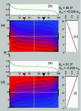
The results presented in Fig. 3 display the normal expected behavior for a 2D Hall effect device with increasing Hall angle. Such simulations can also be utilized to examine the influence of microwave excitation since microwaves modify the diagonal conductivity, , or resistivity, ,grid23 ; grid33 and this sets via . In the next figure, we examine the results of such simulations when the diagonal conductivity, , reverses signs and takes on negative values, as per theory, under microwave excitation. Thus, figure 4 compares the potential profile within the Hall bar device for positive () and negative () values of the conductivity.
Fig. 4(a) shows the potential profile at . This figure is identical to the figure exhibited in Fig. 3(g). The essential features are that the equipotential contours are nearly parallel to the long axis of the Hall bar, see Fig. 4(b), signifying a reduced diagonal resistance. Concurrently, Fig. 4(c) suggests the development of a large Hall voltage between the bottom and top edges. Here the Hall voltage decreases from the bottom- to the top- edge.
Fig. 4(d) shows the potential profile at , i.e., the negative conductivity case. The important feature here is the reflection of the potential profile with respect Fig. 4(a) about the line at when the shifts from a positive () to a negative () value. Fig. 4(e) shows, remarkably, that in the negative condition, the potential still decreases from left to right, implying and even in this condition. Fig. 4(f) shows that for , the potential increases from the bottom edge to the top edge, in sharp contrast to Fig. 4(c). Thus, these simulations show clearly that the Hall voltage undergoes sign reversal when , although the diagonal voltage (and resistance) exhibits positive values.
II Discussion
Existing theory indicates that photo-excitation of the high mobility 2D electron system can drive the and to negative values at the minima of the radiation-induced oscillatory magneto-resistivity.grid23 ; grid25 ; grid27 ; grid111 ; grid46 ; grid33 Andreev et al.,grid24 have argued that ” by itself suffices to explain the zero-dc-resistance state” because ”negative linear response conductance implies that the zero-current state is intrinsically unstable.” Since our simulations (Fig. 4) show clearly that negative magneto conductivity/resistivity leads to positive, not negative, conductance/resistance, it looks like one cannot argue for an instability in the zero-current state based on presumed ”negative linear response conductance.”
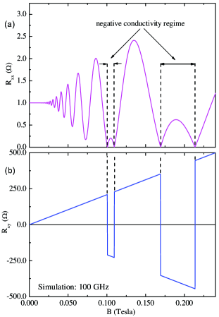
For illustrative purposes, using the understanding obtained from the simulation results shown in Fig. 4, we sketch in Fig. 5 the straightforward expectations, for the behavior of the diagonal () and Hall () resistances in a 2D system driven periodically to negative diagonal conductivity by photo-excitation. Fig. 5(a) shows that the microwave-induced magnetoresistance oscillations in grow in amplitude with increasing . When the oscillations in the magneto-resistivity/conductivity are so large that the oscillatory minima would be expected to cross into the regime of at the oscillatory minima, the exhibits positive values. Here, vanishing occurs only at singular values of the magnetic field where . Fig. 5(b) shows that the Hall resistance shows sign reversal over the same span of where .
It appears that if there were an instability, it should be related to the sign-reversal in the Hall effect. Yet, note that sign reversal in the Hall effect is not a manifestly un-physical effect since it is possible to realize Hall effect sign reversal in experiment even with a fixed external bias on the sample, as in the simulations, simply by reversing the direction of the magnetic field or by changing the sign of the charge carriers. The unusual characteristic indicated by these simulations is Hall effect sign reversal even without changing the direction of the magnetic field or changing the sign of the charge carriers. This feature can be explained, however, by noting that the numerical solution of the boundary value problem depends on a single parameter, the Hall angle, , where . Since this single parameter depends on the ratio of the off-diagonal and diagonal conductivities, sign change in produces the same physical effect as sign reversal in so far as the solution to the boundary value problem is concerned. That is, one might change the sign of or one might change the sign of , the end physical result is the same: a sign reversal in the Hall effect.
One might also ask: why do the simulations indicate a positive diagonal resistances for the negative diagonal conductivity/resistivity scenario? The experimental setup shown in Fig. 2 offers an answer to this question: In the experimental setup, the Hall bar is connected to an external battery which enforces the direction of the potential drop from one end of the specimen to the other. This directionality in potential drop is also reflected in the boundary value problem. As a consequence, the red potential probe in Fig. 2, 3 or 4 would prefer to show a higher potential than the black potential probe so long as the is not identically zero, and this leads to the positive resistance even for negative diagonal conductivity/resistivity in the numerical simulations.
We remark that the experimental results of Fig. 1(a) are quite unlike the expectations exhibited in Fig. 5. Experiment shows an ordinary Hall effect without anomalies over the zero-resistance region about , not a sign reversal in the Hall effect, and experiment shows zero-resistance, not the positive resistance expected for a system driven to negative conductivity.
In conclusion, the results presented here suggest that a bare negative magneto- conductivity/resistivity state in the 2DES under photo-excitation should yield a positive diagonal resistance with a concomitant sign reversal in the Hall effect.
We have also understood that these results could be potentially useful for understanding plateau formation in the Hall effect as, for example, in the quantum Hall situation, if new physics comes into play in precluding sign reversal in the Hall effect, when the diagonal magneto-conductivity/resistivity is forced into the regime of negative values.
III Methods
III.1 Samples
The GaAs/AlGaAs material utilized in our experiments exhibit electron mobility and electron density in the range . Utilized devices include cleaved specimens with alloyed indium contacts and Hall bars fabricated by optical lithography with alloyed Au-Ge/Ni contacts. Standard low frequency lock-in techniques yield the electrical measurements of and .grid1 ; grid3 ; grid4 ; grid201 ; grid202 ; grid5 ; grid11 ; grid209 ; grid203 ; grid16 ; grid16b ; grid21 ; grid21y ; grid60 ; grid61 ; grid108 ; grid109
III.2 Microwave transport measurements
Typically, a Hall bar specimen was mounted at the end of a long straight section of a rectangular microwave waveguide. The waveguide with sample was inserted into the bore of a superconducting solenoid, immersed in pumped liquid Helium, and irradiated with microwaves, at a source-power mW, as in the usual microwave-irradiated transport experiment.grid1 The applied external magnetic field was oriented along the solenoid and waveguide axis.
References
- (1) Mani, R. G. et al. Zero-resistance states induced by electromagnetic-wave excitation in GaAs/AlGaAs heterostructures. Nature (London) 420, 646 (2002).
- (2) Zudov, M. A., Du, R. R., Pfeiffer, L. N., & West, K. W. Evidence for a new dissipationless effect in 2D electronic transport. Phys. Rev. Lett. 90, 046807 (2003).
- (3) Mani, R. G. et al. Radiation induced oscillatory Hall effect in high mobility GaAs/AlGaAs devices. Phys. Rev. B 69, 161306 (2004);
- (4) Mani, R. G. et al. Demonstration of a 1/4 cycle phase shift in the radiation-induced oscillatory-magnetoresistance in GaAs/AlGaAs devices. Phys. Rev. Lett. 92, 146801 (2004).
- (5) Mani, R. G. et al. Radiation induced zero-resistance states in GaAs/AlGaAs heterostructures: Voltage-current characteristics and intensity dependence at the resistance minima. Phys. Rev. B 70, 155310 (2004).
- (6) Mani, R. G. et al. Radiation-induced oscillatory magnetoresistance as a sensitive probe of the zero-field spin splitting in high-mobility GaAs/AlGaAs devices. Phys. Rev. B 69, 193304 (2004).
- (7) Mani, R. G. Zero-resistance states induced by electromagnetic-wave excitation in GaAs/AlGaAs heterostructures. Physica E (Amsterdam) 22, 1-6 (2004).
- (8) Studenikin, S. A., Potemski, M., Coleridge, P. T., Sachrajda, A. S. & Wasilewski, Z. R. Microwave radiation induced magneto-oscillations in the longitudinal and transverse resistance of a two-dimensional electron gas. Sol. St. Comm. 129, 341-345 (2004).
- (9) Kovalev, A. E., Zvyagin, S. A., Bowers, C. R., Reno, J. L. & Simmons, J. A. Observation of a node in the quantum oscillations induced by microwave radiation. Sol. St. Comm. 130, 379-381 (2004).
- (10) Willett, R. L., Pfeiffer, L. N. & K. W. West, Evidence for current flow anomalies in the irradiated 2D electron system at small magnetic fields. Phys. Rev. Lett. 93, 026804 (2004).
- (11) Du R. R., et al., Dissipationless 2D electronic transport effect induced by microwaves. Physica E (Amsterdam) 22, 7-12 (2004).
- (12) Mani, R. G. Novel zero-resistance states induced by photoexcitation in the high mobility GaAs/AlGaAs two-dimensional electron system. Physica E (Amsterdam) 25, 189-197 (2004).
- (13) Mani, R. G. Radiation-induced zero-resistance states with resolved Landau levels. Appl. Phys. Lett. 85, 4962-4964 (2004);
- (14) Mani, R. G. Radiation-induced oscillatory magnetoresistance in a tilted magnetic field in GaAs/AlGaAs devices. Phys. Rev. B 72, 075327 (2005);
- (15) Simovic, B., Ellenberger, C., Ensslin, K. & Wegscheider, W. Density dependence of microwave induced magnetoresistance oscillations in a two-dimensional electron gas. Phys. Rev. B 71, 233303 (2005).
- (16) Smet, J. H. et al. Circular-polarization-dependent study of the microwave photoconductivity in a two-dimensional electron system. Phys. Rev. Lett. 95, 116804 (2005).
- (17) Yuan, Z. Q., Yang, C. L., Du, R. R., Pfeiffer, L. N. & West, K. W. Microwave photoresistance of a high mobility two-dimensional electron gas in a triangular antidot lattice. Phys. Rev. B 74, 075313 (2006).
- (18) Mani, R. G. Radiation-induced decay of Shubnikov-de Haas oscillations in the regime of the radiation-induced zero-resistance states. Appl. Phys. Lett. 91, 132103 (2007).
- (19) Studenikin, S. A. et al. Frequency quenching of microwave-induced resistance oscillations in a high mobility two-dimensional electron gas. Phys. Rev. B 76, 165321 (2007).
- (20) Wirthmann, A. Far-infrared-induced magnetoresistance oscillations in GaAs/AlGaAs-based two-dimensional electron systems. et al. Phys. Rev. B 76, 195315 (2007).
- (21) Wiedmann, S. et al. Interference oscillations of microwave photoresistance in double quantum wells. Phys. Rev. B 78, 121301(R) (2008).
- (22) Mani, R. G. Narrow-band radiation-sensing in the Terahertz and microwave bands using the radiation-induced magnetoresistance oscillations. Appl. Phys. Lett. 92, 102107 (2008).
- (23) Mani, R. G. Evolution of Shubnikov-de Haas oscillations under photoexcitation in the regime of the radiation-induced zero-resistance states. Physica E 40, 1178-1181 (2008).
- (24) Mani, R. G., Johnson, W. B., Umansky, V., Narayanamurti, V. & Ploog, K. Phase study of oscillatory resistances in microwave irradiated and dark GaAs/AlGaAs devices: Indications of an unfamiliar class of integral quantum Hall effect. Phys. Rev. B 79, 205320 (2009).
- (25) Wiedmann, S. et al. Magnetoresistance oscillations in multilayer systems: Triple quantum wells. Phys. Rev. B 80, 245306 (2009).
- (26) Konstantinov, D. & Kono, K. Photon-induced vanishing of magnetoconductance in 2D electrons on liquid helium. Phys. Rev. Lett. 105, 226801 (2010).
- (27) Mani, R. G., Gerl, C., Schmult, S., Wegscheider, W. & Umansky, V. Nonlinear growth with the microwave intensity in the radiation-induced magnetoresistance oscillations. Phys. Rev. B 81, 125320 (2010).
- (28) Fedorych, O. M. et al. Quantum oscillations in the microwave magnetoabsorption of a two-dimensional electron gas. Phys. Rev. B 81, 201302 (2010).
- (29) Ramanayaka, A. N., Mani, R. G. & Wegscheider, W. Microwave induced electron heating in the regime of the radiation-induced magnetoresistance oscillations. Phys. Rev. B 83, 165303 (2011).
- (30) Wiedmann, S. Microwave-induced Hall resistance in bilayer electron systems. et al. Phys. Rev. B 83, 195317 (2011).
- (31) Mani, R. G., Ramanayaka, A. N., and Wegscheider, W. Observation of linear-polarization-sensitivity in the microwave-radiation-induced magnetoresistance oscillations. Phys. Rev. B 84, 085308 (2011).
- (32) Ramanayaka, A. N., Mani, R. G., Inarrea, J. & Wegscheider, W. Effect of rotation of the polarization of linearly polarized microwaves on the radiation-induced magnetoresistance oscillations. Phys. Rev. B 85, 205315 (2012).
- (33) Bogan, A. et al. Microwave-induced resistance oscillations in tilted magnetic fields. Phys. Rev. B 86, 235305 (2012).
- (34) Mani, R. G., Hankinson, J., Berger, C. & de Heer, W. A. Observation of resistively detected hole spin resonance and zero-field pseudo-spin splitting in graphene. Nature Commun. 3, 996 doi: 10.1038/ncomms1986 (2012).
- (35) Ye, T., Mani, R. G., & Wegscheider, W. Remotely sensed transport in microwave photoexcited GaAs/AlGaAs two-dimensional electron system. Appl. Phys. Lett. 102, 242113 (2013).
- (36) Mani, R. G. et al. Terahertz photovoltaic detection of cyclotron resonance in the regime of the radiation-induced magnetoresistance oscillations. Phys. Rev. B 87, 245308 (2013).
- (37) Durst, A. C., Sachdev, S., Read, N. & Girvin, S. M. Radiation-induced magnetoresistance oscillations in a 2D electron gas, Phys. Rev. Lett. 91, 086803 (2003).
- (38) Andreev, A. V., Aleiner, I. L. & Millis, A. J. Dynamical symmetry breaking as the origin of the zero-dc-resistance state in an ac-driven system. Phys. Rev. Lett. 91, 056803 (2003).
- (39) Ryzhii, V. & Suris, R. Nonlinear effects in microwave photoconductivity of two-dimensional electron systems. J. Phys.: Cond. Matt. 15, 6855-6869 (2003).
- (40) Koulakov, A. A. & Raikh, M. E. Classical model for the negative dc conductivity of ac-driven two-dimensional electrons near the cyclotron resonance. Phys. Rev. B 68, 115324 (2003).
- (41) Lei, X. L. & Liu, S. Y. Radiation-induced magnetoresistance oscillation in a two-dimensional electron gas in Faraday geometry. Phys. Rev. Lett. 91, 226805 (2003).
- (42) Rivera, P. H. & Schulz, P. A. Radiation-induced zero-resistance states: Possible dressed electronic effects. Phys. Rev. B 70, 075314 (2004).
- (43) Lei, X. L. Theoretical analysis of radiation-induced magnetoresistance oscillations in high mobility two-dimensional electron systems. J. Phys.: Condens. Matter 16, 4045-4060 (2004).
- (44) Mikhailov, S. A. Microwave-induced magnetotransport phenomena in two-dimensional electron systems: Importance of electrodynamic effects. Phys. Rev. B 70, 165311 (2004).
- (45) Torres, M. & Kunold, A. Kubo formula for Floquet states and photoconductivity oscillations in a two-dimensional electron gas. Phys. Rev. B71, 115313 (2005).
- (46) Inarrea, J. & Platero, G. Temperature effects on microwave-induced resistivity oscillations and zero-resistance states in two-dimensional electron systems. Phys. Rev. B 72, 193414 (2005).
- (47) Lei, X. L. & Liu, S. Y. Radiation-induced magnetotransport in high mobility two-dimensional systems: Role of electron heating. Phys. Rev. B 72, 075345 (2005).
- (48) Dmitriev, I. A., Vavilov, M. G., Aleiner, I. L., Mirlin, A. D. & Polyakov, D. G. Theory of microwave-induced oscillations in the magnetoconductivity of a two-dimensional electron gas. Phys. Rev. B 71, 115316 (2005).
- (49) Inarrea, J. & Platero, G. Theoretical approach to microwave radiation-induced zero-resistance states in 2D electron systems. Phys. Rev. Lett. 94, 016806 (2005).
- (50) Auerbach, A., Finkler, I., Halperin, B., & Yacoby, A., Steady states of a microwave irradiated quantum-Hall gas. Phys. Rev. Lett. 94, 196801 (2005).
- (51) Inarrea, J. & Platero, G. Polarization immunity of magnetoresistivity response under microwave irradiation. Phys. Rev. B 76, 073311 (2007);
- (52) Inarrea, J. & Platero, G. Effect of an inplane magnetic field on microwave assisted magnetotransport in a two-dimensional electron system. Phys. Rev. B 78, 193310 (2008).
- (53) Auerbach, A. & Pai, G. V. Nonlinear current of strongly irradiated quantum Hall gas. Phys. Rev. B 76, 205318 (2007).
- (54) Dmitriev, I. A., Mirlin, A. D. & Polyakov, D. G. Microwave photoconductivity of a two-dimensional electron gas: Mechanisms and their interplay at high radiation power. Phys. Rev. B 75, 245320 (2007).
- (55) Rivera, P. H., Pereira, A. L. C. & Schulz, P. A. Quasienergy spectra of graphene dots in intense ac fields: Field anisotropy and photon-dressed quantum rings. Phys. Rev. B 79, 205406 (2009).
- (56) Finkler, I. G. & Halperin, B. I. Microwave-induced zero-resistance states are not necessarily static. Phys. Rev. B 79, 085315 (2009).
- (57) Lei, X. L. & Liu, S. Y. Temperature dependence of microwave-induced magnetoresistance oscillation in two-dimensional electron system. Appl. Phys. Lett. 94, 232107 (2009).
- (58) Chepelianskii, A. D. & Shepelyansky, D. L. Microwave stabilization of edge transport and zero-resistance states. Phys. Rev. B 80, 241308(R) (2009).
- (59) Dmitriev, I. A., Khodas, M., Mirlin, A. D., Polyakov, D. G. & Vavilov, M. G. Mechanisms of the microwave photoconductivity in two-dimensional electron systems with mixed disorder. Phys. Rev. B 80, 165327 (2009).
- (60) Toyoda, T. Fermi liquid model of radiation induced magnetoresistance oscillations in GaAs/AlGaAs heterostructure two-dimensional electron system. Mod. Phys. Lett. B 24, 1923 (2010).
- (61) Inarrea J. et al. Sublinear radiation power dependence of photoexcited resistance oscillations in two-dimensional electron systems. Phys. Rev. B 82, 205321 (2010).
- (62) Mikhailov, S. A. Theory of microwave-induced zero-resistance states in two-dimensional electron systems. Phys. Rev. B 83, 155303 (2011).
- (63) Inarrea, J. Influence of linearly polarized radiation on magnetoresistance in irradiated two-dimensional electron systems. Appl. Phys. Lett. 100, 242103 (2012).
- (64) Lei X. L. & Liu, S. Y. Linear polarization dependence of microwave-induced magnetoresistance oscillations in high mobility two-dimensional systems. Phys. Rev. B 86, 205303 (2012).
- (65) Inarrea, J. Microwave-induced resistance oscillations and zero resistance states in 2D bilayer systems. Nanosc. Res. Lett. 8, 259 (2013).
- (66) Zhirov, O. V., Chepelianskii, A. D. & Shepelyansky, D. L. Towards a synchronization theory of microwave-induced zero-resistance states. Phys. Rev. B 88, 035410 (2013).
- (67) Newsome J. P. & Silber, W. H. The resistance matrix and electrical characteristics of the symmetrical rectangular Hall plate with different electrode configurations. Sol. St. Elect. 12, 631-634 (1969).
- (68) Mani, R. G. Transport study of GaAs/AlGaAs heterostructure and n-type GaAs-devices in the ”anti-Hall bar within a Hall bar” configuration. J. Phys. Soc. Jpn. 65, 1751-1759 (1996).
- (69) Oswald, M., Oswald, J. & Mani, R. G. Voltage and current distribution in a doubly connected two-dimensional quantum Hall system. Phys. Rev. B 72, 035334 (2005).
IV Acknowledgements
The basic research at Georgia State University is primarily supported by the U.S. Department of Energy, Office of Basic Energy Sciences, Material Sciences and Engineering Division under DE-SC0001762. Additional support is provided by the ARO under W911NF-07-01-015.