Plasmonic Nature of the Terahertz Conductivity Peak in Single-Wall
Carbon Nanotubes
Abstract
Plasmon resonance is expected to occur in metallic and doped semiconducting carbon nanotubes in the terahertz frequency range, but its convincing identification has so far been elusive. The origin of the terahertz conductivity peak commonly observed for carbon nanotube ensembles remains controversial. Here we present results of optical, terahertz, and DC transport measurements on highly enriched metallic and semiconducting nanotube films. A broad and strong terahertz conductivity peak appears in both types of films, whose behaviors are consistent with the plasmon resonance explanation, firmly ruling out other alternative explanations such as absorption due to curvature-induced gaps.
I Introduction
Understanding the dynamic and plasmonic properties of charge carriers in single-wall carbon nanotubes (SWCNTs) is crucial for emerging applications of SWCNT-based ultrafast electronics and optoelectronics devices,Avouris et al. (2008); Nanot et al. (2012) especially in the terahertz (THz) range.Portnoi et al. (2008); Ren et al. (2012a) SWCNTs with different chiralities exhibit either semiconducting or metallic properties, providing great flexibility for a variety of THz and plasmonic applications, including sources,Portnoi et al. (2006); Kibis et al. (2007); Nemilentsau et al. (2007) detectors,Portnoi et al. (2006, 2008) antennas,Hanson (2005); Burke et al. (2006) and polarizers.Ren et al. (2009); Kyoung et al. (2011); Ren et al. (2012b) A pronounced, finite-frequency peak in THz conductivity spectra has been universally observed in diverse types of SWCNT samples, containing both semiconducting and metallic nanotubes.Bommeli et al. (1996); Ugawa et al. (1999); Itkis et al. (2002); Jeon et al. (2002, 2004, 2005); Akima et al. (2006); Borondics et al. (2006); Nishimura et al. (2007); Kampfrath et al. (2008); Slepyan et al. (2010); Pekker and Kamarás (2011); Shuba et al. (2012); Ren et al. (2013) Two interpretations have emerged regarding the THz peak, but there is no consensus about its origin. One of the possible mechanisms proposed by many authorsUgawa et al. (1999); Borondics et al. (2006); Nishimura et al. (2007); Kampfrath et al. (2008) is based on interband absorption across the curvature-induced bandgapHamada et al. (1992); Kane and Mele (1997) in non-armchair metallic SWCNTs, while the other is the plasmon resonance in metallic and doped semiconducting SWCNTs due to their finite lengths.Jeon et al. (2002); Akima et al. (2006); Slepyan et al. (2010); Shuba et al. (2012); Nakanishi and Ando (2009) Hence, spectroscopic studies of type-sorted SWCNT samples are crucial for determining which of the two working hypotheses is correct.
In the first scenario, direct interband absorption occurs across the narrow bandgapHamada et al. (1992); Kane and Mele (1997); Ouyang et al. (2001) induced by lattice distortion in the rolled-up graphene sheet in non-armchair metallic SWCNTs. The magnitude of the induced bandgap is given byKane and Mele (1997) = , where = 0.142 nm is the interatomic distance in graphene, is the nanotube diameter, 3.2 eV is the tight-binding transfer integral, and is the chiral angle. For a SWCNT with 1.5 nm and 0, 20 meV.Hároz et al. (2013) If this scenario is correct, the THz peak should (1) appear only in non-armchair () metallic SWCNTs, (2) show a sensitive dependence on ,Pekker and Kamarás (2011) (3) be suppressed by doping or optical pumping,Kampfrath et al. (2008) have a strong (4) temperature dependence and (5) polarization dependence. It is also important to note that no detailed theory exists for predicting the lineshape for interband absorption in non-armchair metallic SWCNTs including excitonic effects.Ando (1997); Hartmann et al. (2011)
In the second scenario, THz radiation incident onto a finite-length metallic or doped semiconducting SWCNT launches collective charge oscillations (plasmons) along the nanotube axis with a frequency given by the charge density and nanotube length. The expected experimental signatures of this process are: (1) the THz peak should be observable both in metallic and doped semiconducting nanotubes; (2) the frequency of the THz peak should systematically depend on the nanotube length in a predictable manner;Nakanishi and Ando (2009); Shuba et al. (2012) (3) the THz peak intensity should be enhanced by doping in semiconducting SWCNTs; (4) there should be weak temperature dependence;Ugawa et al. (1999) and (5) there should be strong polarization dependence, with no resonance expected for polarization perpendicular to the nanotube axis.
To systematically prove or disprove these scenarios, broadband spectroscopic studies on well-separated semiconducting and metallic SWCNT samples are necessary.Ichida et al. (2011) In particular, in order to correctly interpret THz spectra, it is important to monitor interband transitions in the near-infrared (NIR), visible (VIS), and ultraviolet (UV). Hence, we performed absorption spectroscopy studies from the THz to the UV as well as DC transport measurements on highly-enriched semiconducting and metallic SWCNT films. We clearly observed a broad and pronounced THz peak in both types of films. However, in semiconductor-enriched films, the peak significantly decreased in intensity after carriers were removed by annealing. In both types of films, the THz peak showed a very weak temperature dependence. These observations led us to conclude that this peak is due to plasmon resonance of free carriers in metallic and doped semiconducting nanotubes, rather than interband absorption in non-armchair metallic nanotubes.
II Methods
Suspensions enriched in metallic and semiconducting types of SWCNTs were produced via density gradient ultracentrifugation (DGU)Arnold et al. (2005, 2006); Yanagi et al. (2008); Hároz et al. (2010, 2012, 2013) using a three-surfactant system. Arc-discharge-P2-SWNT grade (Carbon Solutions, Inc.) SWCNTs were initially dispersed in 1% (wt./vol.) sodium deoxycholate (DOC) (sodium deoxycholate monohydrate, Aldrich, 97% purity) by bath sonication (Cole-Parmer 60 W ultrasonic cleaner, model #08849-00) for 30 minutes at a starting concentration of SWCNTs of 1 g/L. The suspension was then further sonicated by probe ultrasonicator (Cole-Parmer 500 W ultrasonic processor, model # CPX-600, 1/4” probe, 35% amplitude) for 6 hours while being cooled in a water bath maintained at 10∘C. Lastly, the suspension was then centrifuged for 1 hour at 208,400g average (Sorvall Discovery 100SE Ultracentrifuge using a Beckman SW-41 Ti swing bucket rotor) to remove large bundles of SWCNTs. After centrifugation, the upper 80% of the supernatant was removed for use in DGU.
For DGU, a mass density gradient was prepared composed of 1.5% (wt./vol.) sodium dodecyl sulfate (SDS) (sodium dodecyl sulfate- molecular biology or electrophoresis grade, Sigma, 99% purity), 1.5 % (wt./vol.) sodium cholate (SC) (sodium cholate hydrate, Aldrich, 98% purity), and varying amounts of iodixanol (Opti-Prep density gradient medium, Sigma, 60% (wt./vol.) solution in water). The gradient was layered inside a centrifuge tube in 2 mL volume steps starting from the bottom with 40% (wt./vol.), 30% (wt./vol.), 27.5% (wt./vol.), 25% (wt./vol.), 22.5% (wt./vol.), and 20% (wt./vol.) iodixanol. All gradient steps except the 40% layer contained 1.5% (wt./vol.) SDS and 1.5% (wt./vol.) SC. The 40% layer, which contained SWCNTs, was prepared by vortex mixing (Fisher Scientific Vortex Genie 2, model # 12-812, mixed at maximum setting) for 2 minutes 0.67 mL of the SWCNT supernatant prepared previously with 1.33 mL of 60% iodixanol, 1.5% SDS, and 1.5% SC to ultimately form 2 mL of 40% iodixanol, 1% SDS, 1% SC, and 0.33% DOC. The gradient was then centrifuged for 18 hours at 208,400g average (Beckman SW-41 Ti swing bucket rotor). The top 250 L of the metal-enriched (aqua green-blue-colored) fractions and semiconductor-enriched (rust-colored) fractions were extracted by hand-pipetting for measurements of suspension samples.
For the preparation of film samples, vacuum filtration was performed on enriched SWCNT suspensions using a procedure modified from one previously described.Dan et al. (2012) Briefly, 8 mL of enriched SWCNT suspension was vacuum-filtered using 50 nm-pore size, polycarbonate filtration membranes. After filtration was finished and the film was dried, the film was washed by alternating filtrations of 50 mL of boiling nanopure water and 50 mL of 50%/50% vol. ethanol/nanopure water through the SWCNT film and filtration membrane. This was repeated three times to remove surfactants and iodixanol. Finally, the films were immersed in bath of N-methyl-2-pyrrolidone (NMP) to dissolve away the filtration membrane and transferred onto intrinsic silicon and sapphire substrates for optical measurements. The thickness of semiconductor- and metal-enriched films were measured via vertical scanning interferometry to be 410 nm and 190 nm, respectively. Annealing of prepared nanotube films was done in a vacuum quartz tube furnace at a base pressure of 3 10-6 Torr. The films were initially heated to 423 K, 573 K, and lastly 823 K. At each temperature, the films remained at that temperature until no other chemical species were observed to desorb as determined by a monitoring furnace pressure. Upon completion of annealing, the films were brought back to room temperature under vacuum and then subsequently exposed to the atmosphere.
For obtaining attenuation spectra in a transmission geometry in a wide spectral range, we used time-domain THz spectroscopy (TDTS) in the 0.15-2.5 THz range, Fourier-transform infrared spectroscopy (FTIR, Jasco-660) in the 3-300 THz range, and a UV-VIS-NIR double beam spectrophotometer (Shimadzu UV-3101PC scanning spectrophotometer) in the 300-1200 THz range (250-1000 nm in wavelength). The TDTS setup used a ZnTe crystal for THz generation and photoconductive antennas for detection with a 150 fs Ti:sapphire laser. DC transport studies were performed on the same films via four-point measurements with gold ohmic contacts under a nitrogen environment.
III Results
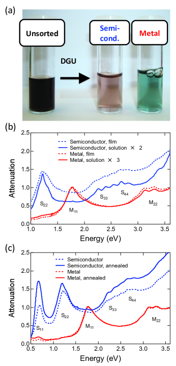
As shown in Figure 1a, different coloration occurs between the metal- and semiconductor-enriched solutions due to the subtraction of different colors by distinct interband transitions.Hároz et al. (2012) Figure 1b presents the attenuation, , where is the transmittance, in the NIR-VIS-UV range for solution and film samples of SWCNTs. The M11 and M22 (S22, S33, and S44) interband transitions are absent in the semiconductor (metal) case. The semiconductor-enriched solution (blue solid line) exhibits sharp features, coming from different (,) species, which are not resolved in the corresponding film (blue dashed line). This is expected because the nanotubes are individually suspended in the solution while they are bundled in the film, which broadens interband absorption peaks. However, interestingly, in the metallic case, bundling-induced broadening seems non-existent, i.e., the M11 and M22 peaks maintain their shapes between the solution (red solid curve) and film (red dashed curve) forms.
Figure 1c shows the effect of annealing on the attenuation spectra of semiconductor- and metal-enriched films from the mid-infrared (MIR) to the UV, again showing the robustness of the interband features of metallic SWCNTs. The films were vacuum annealed (see Section II for the annealing conditions used) to remove the adsorbed molecules that act as dopants to provide carriers.Zahab et al. (2000); Kang et al. (2005) The removal of carriers results in an enhancement of the S11 peak as well as a small (20 meV) red shift of both the S11 and S22 peaks. We interpret these annealing-induced spectral changes in the semiconducting film in terms of Pauli blocking and bandgap renormalization; namely, before annealing, carriers occupy some near-band-edge states, which not only prevent interband transitions but also modify the bandgap via many-body interactions. On the contrary, there are basically no doping effects in the metallic film, except the change seen in the S11 region due to a small amount (estimated to be 5%) of residual semiconducting SWCNTs.
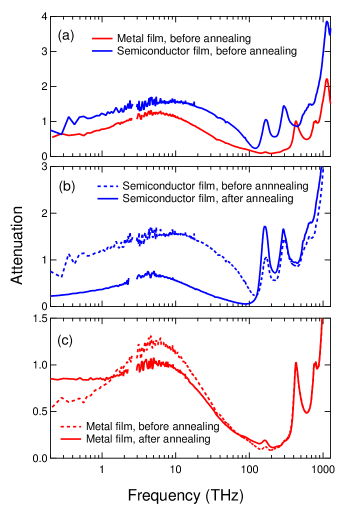
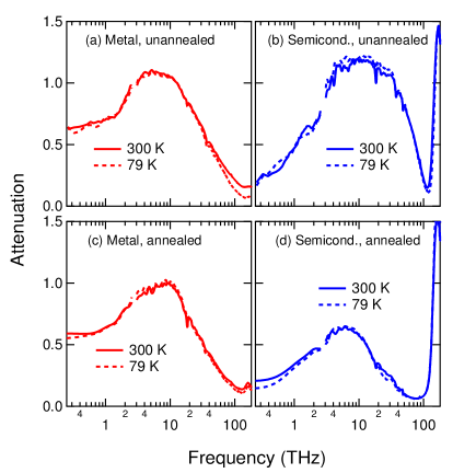
Attenuation spectra of the semiconductor- and metal-enriched SWCNT films at room temperature in a very broad spectral range, from the THz to the UV, are shown in Figure 2a, demonstrating the existence of a broad and pronounced THz peak in both types of films; the peak is slightly smaller in width and lower in frequency in the metallic film. Annealing effects are strikingly different between the two types of films: in the semiconducting film (Figure 2b), the THz peak is significantly suppressed by carrier removal, whereas in the metallic film (Figure 2c), the THz peak exhibits a small decrease in intensity at its peak position but there is an increase in absorption at the lowest frequency side of the spectrum toward DC. Note that the sharp features above 100 THz are interband transitions (S11, S22, S33, M11, and M22), whose behaviors upon annealing are discussed in the last paragraph. Furthermore, we performed temperature-dependent spectroscopy of this broad THz peak down to 79 K, as shown in Figure 3. There is very little spectral change between 300 K and 79 K for both before (Figures 3a and 3b) and after (Figures 3c and 3d) annealing in both metallic (Figures 3a and 3c) and semiconducting (Figures 3b and 3d) nanotubes.
IV Discussion
Based on these observations, we can rule out the curvature-induced gap interpretation for the appearance of the THz peak. There are three lines of argument that strongly support this conclusion. First, interband transitions for curvature-induced gaps should exist only in metallic samples. However, the THz peak clearly appears in the semiconducting film with a strength comparable to that in the metallic film. Second, an optical excitation across a 20 meV gap should be extremely sensitive to carrier doping due to Pauli blocking. The nanotubes need to be almost intrinsic in order to make the curvature-gap transition dominate the low-energy excitation. Our data show the opposite: doping semiconducting nanotubes enhances the THz peak. In the metallic film (which contains non-armchair metallic nanotubes), on the other hand, doping has only small influence. Third, a very weak temperature dependence was observed for the THz peak. A curvature-induced gap is calculated to be 0-20 meV (0 for armchair and 20 meV for zigzag tubes) for the metallic nanotubes used in this study ( 1.5 nm),Hároz et al. (2013) which is comparable with or much less than the room temperature thermal energy (26 meV). Therefore, such interband absorption is expected to be very sensitive to the thermal carrier distribution, in contradiction with our observation.
Our observations are qualitatively consistent with the plasmon resonance interpretation. In particular, the THz peak is observed both in metallic and doped semiconducting nanotubes, its intensity is enhanced by doping in semiconducting SWCNTs, and there is no temperature dependence. Also, strong polarization dependence has been universally confirmed by many authors, with no resonance expected for polarization perpendicular to the nanotube axis.Jeon et al. (2002); Akima et al. (2006); Ren et al. (2013)
To gain more quantitative understanding via comparison with theoretical models, we performed Kramers-Kronig (KK) transformation on our broadband transmission spectra and obtained the phase spectra .Borondics et al. (2006); Pekker and Kamarás (2011); Dressel and Grüner (2002) We first interpolated the data in the region between the THz and IR and then applied four-pass binomial smoothing to prevent spikes. On the UV side, we extrapolated by using , where is a real constant and is around . We chose and to make the extrapolation as continuous and smooth as possible. On the THz side, we did linear extrapolation of to the zero frequency. Finally, by using
| (1) |
we were able to obtain the phase spectrum, . With and , we obtained the transmission coefficient, .
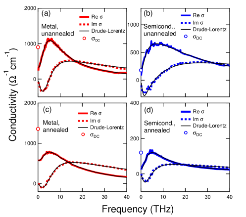
We then converted the transmission coefficient, , into the complex optical conductivity, , through under the thin-film approximation,Nuss and Orenstein (1998) which is valid from DC to the MIR in our case. Here, = 377 is the vacuum impedance, is the film thickness, and is the substrate refractive index. The real and imaginary parts of are plotted in Figure 4 for both films for both before and after annealing. One immediately notices the asymmetric lineshape of the THz peak: the conductivity decays more slowly on the high frequency side. It is also noticeable that each trace has a finite conductivity in the DC limit, whose trend agrees with our DC transport measurements. Annealing results in changes in the DC values, also consistent with the results. The quantitative difference is likely due to the inhomogeneity of the current distribution in the DC measurements; THz radiation acts as a local probe, which is not sensitive to macroscopic inhomogeneity.
The observed asymmetric lineshape cannot be reproduced by a single Lorentzian representing the plasmon resonance; it also cannot be fitted by the Drude-Smith model representing carrier localization.Smith (2001) The finite DC conductance proves the existence of macroscopic percolating conduction channels. Namely, our film cannot be treated as a network of isolated nanotubes (or nanotube bundles) surrounded by air; a correct model has to take into account the intertube transport responsible for the finite macroscopic DC conductance. Therefore, we take into account two effects in our model to describe the experimental optical conductivity: (1) plasmon resonance, which represents the confined collective motion of carriers in the tube-length scale, and (2) Drude-like free carrier response, which describes the intertube transport and percolating channels in the macroscopic scale. The fitting equation we use is
| (2) |
where the first (second) term represents the contribution from the plasmon resonance (the Drude-like free electron response), is the plasmon conductivity at the resonance frequency (), and is the Drude conductivity in the DC limit. and are phenomenological scattering rates for the plasmon and free election response, respectively. This equation describes the experimental traces well, as shown in Figure 4. The extracted fitting parameters are listed in Table 1.
| Semiconductor | Metal | Semiconductor | Metal | |
|---|---|---|---|---|
| annealed | annealed | |||
| (102 cm-1) | 5.00.1 | 7.90.3 | 0.910.1 | 2.50.1 |
| (102 cm-1) | 1.30.1 | 2.80.1 | 0.280.05 | 5.60.1 |
| 2 (THz) | 6.60.2 | 5.50.1 | 5.10.1 | 5.50.1 |
| (THz) | 15210 | 725 | 735 | 665 |
| (THz) | 30020 | 14210 | 22020 | 14010 |
| (102 cm-1) | 1.80.1 | 8.90.1 | 1.20.1 | 14.00.1 |
The plasmon resonance frequency for a SWCNT with length is given by = , where is the mode velocity, which is equal to , where is the Fermi velocity, is the static dielectric constant, and and are the first and second type, respectively, of the modified Bessel function.Nakanishi and Ando (2009) Using = 108 cm/s, = 2.5,Taft and Philipp (1965) = 1.5 nm, = 0.142 nm, and 3.2 eV, together with the measured value of = 5.5 THz (for metal-enriched films before and after annealing), we obtain = 340 nm, very close to the typical tube length in our sample (300 nm). This confirms that the THz conductivity peak is due to plasmon resonance. In the semiconductor case, the plasmon resonance occurs at a slightly higher frequency, while the scattering rate is almost as twice large as that in the metal case. After annealing, the residual THz peak in the semiconductor film has and values that are very similar to the metallic film. We thus interpret the residual peak as mainly arising from the residual metallic tubes in the semiconductor enriched films. The ratio between the carrier densities of the annealed semiconductor and metal films, which can be extracted by spectrally integrating the real part of the conductivity, is . This number should be considered to be the upper limit of the residual metallic tubes in the semiconductor-enriched films since it also includes defects-induced doping, which cannot be removed by annealing. In the annealed metal film, the Drude term dominates the low-frequency response ( ), unlike the other three films where . The result indicates that intertube carrier migration is enhanced by the removal of trapped molecules and the annealing-induced nanotube distortion around the junction, which increases the contact area between nanotubes. In addition, the small in the annealed semiconductor film can be understood as the lack of macroscopic percolating channels for the residual metallic nanotubes.
V Conclusions
In summary, we performed transmission spectroscopy over a wide range (from the THz to the UV) as well as DC transport measurements of semiconductor- and metal-enriched SWCNT samples. Our experimental results show that the broad THz peak originates from a plasmon resonance in both the metallic and doped semiconducting carbon nanotubes rather than the interband excitation of the curvature-induced gap in non-armchair metallic nanotubes. Intraband free electron response also contributes to the low-energy excitation spectrum, especially in the metal-enriched film after annealing. Our studies provide fundamental insight into the low-energy excitation in SWCNTs, while the broadband spectroscopy of semiconducting and metallic type-separated nanotube samples also provide basic knowledge useful for emerging applications of SWCNTs in plasmonics and optoelectronics in the technologically important THz frequency range. Future studies on films of SWCNTs enriched in single chiralities should provide further information on the chirality dependence of low-energy excitations in SWCNTs. In particular, samples of single-chirality non-armchair metallic nanotubes, such as (7,4) nanotubes, will be useful for elucidating the nature of interband absorption across the curvature-induced gaps.
Acknowledgements
This work was supported by the Department of Energy (through Grant No. DE-FG02-06ER46308), the National Science Foundation (through Grants No. OISE-0968405 and EEC-0540832), and the Robert A. Welch Foundation (through Grant No. C-1509).
References
- Avouris et al. (2008) P. Avouris, M. Freitag, and V. Perebeinos, Nat. Photon. 2, 341 (2008).
- Nanot et al. (2012) S. Nanot, E. H. Hároz, J.-H. Kim, R. H. Hauge, and J. Kono, Adv. Mater. 24, 4977 (2012).
- Portnoi et al. (2008) M. E. Portnoi, O. V. Kibis, and M. Rosenau da Costa, Superlatt. Micrortruc. 43, 399 (2008).
- Ren et al. (2012a) L. Ren, Q. Zhang, S. Nanot, I. Kawayama, M. Tonouchi, and J. Kono, J. Infrared Milli. Terahz Waves 33, 846 (2012a).
- Portnoi et al. (2006) M. E. Portnoi, O. V. Kibis, and M. Rosenau da Costa, Proc. SPIE 6328, 632805 (2006).
- Kibis et al. (2007) O. V. Kibis, M. Rosenau da Costa, and M. E. Portnoi, Nano Lett. 7, 3414 (2007).
- Nemilentsau et al. (2007) A. M. Nemilentsau, G. Y. Slepyan, and S. A. Maksimenko, Phys. Rev. Lett. 99, 147403 (2007).
- Hanson (2005) G. W. Hanson, IEEE Trans. Antennas Propag. 53, 3426 (2005).
- Burke et al. (2006) P. J. Burke, S. Li, and Z. Yu, IEEE Trans. Nanotechnol. 5, 314 (2006).
- Ren et al. (2009) L. Ren, C. L. Pint, L. G. Booshehri, W. D. Rice, X. Wang, D. J. Hilton, K. Takeya, I. Kawayama, M. Tonouchi, R. H. Hauge, et al., Nano Lett. 9, 2610 (2009).
- Kyoung et al. (2011) J. Kyoung, E.-Y. Jang, M. D. Lima, H.-R. Park, R.-O. Robls, X. Lepro, Y.-H. Kim, R. H. Baughman, and D.-S. Kim, Nano Lett. 11, 4227 (2011).
- Ren et al. (2012b) L. Ren, C. L. Pint, T. Arikawa, K. Takeya, I. Kawayama, M. Tonouchi, R. H. Hauge, and J. Kono, Nano Lett. 12, 787 (2012b).
- Bommeli et al. (1996) F. Bommeli, L. Degiorgi, P. Wachter, W. S. Bacsa, W. A. de Heer, and L. Forro, Solid State Commun. 99, 513 (1996).
- Ugawa et al. (1999) A. Ugawa, A. G. Rinzler, and D. B. Tanner, Phys. Rev. B 60, R11305 (1999).
- Itkis et al. (2002) M. E. Itkis, S. Niyogi, M. E. Meng, M. A. Hamon, H. Hu, and R. C. Haddon, Nano Lett. 2, 155 (2002).
- Jeon et al. (2002) T.-I. Jeon, K.-J. Kim, C. Kang, S.-J. Oh, J.-H. Son, K. H. An, D. J. Bae, and Y. H. Lee, Appl. Phys. Lett. 80, 3403 (2002).
- Jeon et al. (2004) T.-I. Jeon, K.-J. Kim, C. Kang, I. H. Maeng, J.-H. Son, K. H. An, J. Y. Lee, and Y. H. Lee, J. Appl. Phys. 95, 5736 (2004).
- Jeon et al. (2005) T.-I. Jeon, J.-H. Son, K. H. An, Y. H. Lee, and Y. S. Lee, J. Appl. Phys. 98, 034316 (2005).
- Akima et al. (2006) N. Akima, Y. Iwasa, S. Brown, A. M. Barbour, J. Cao, J. L. Musfeldt, H. Matsui, N. Toyota, M. Shiraishi, H. Shimoda, et al., Adv. Mater. 18, 1166 (2006).
- Borondics et al. (2006) F. Borondics, K. Kamarás, M. Nikolou, D. B. Tanner, Z. H. Chen, and A. G. Rinzler, Phys. Rev. B 74, 045431 (2006).
- Nishimura et al. (2007) H. Nishimura, N. Minami, and R. Shimano, Appl. Phys. Lett. 91, 011108 (2007).
- Kampfrath et al. (2008) T. Kampfrath, K. von Volkmann, C. M. Aguirre, P. Desjardins, R. Martel, M. Krenz, C. Frischkorn, M. Wolf, and L. Perfetti, Phys. Rev. Lett. 101, 267403 (2008).
- Slepyan et al. (2010) G. Y. Slepyan, M. V. Shuba, S. A. Maksimenko, C. Thomsen, and A. Lakhtakia, Phys. Rev. B 81, 205423 (2010).
- Pekker and Kamarás (2011) A. Pekker and K. Kamarás, Phys. Rev. B 84, 075475 (2011).
- Shuba et al. (2012) M. V. Shuba, A. G. Paddubskaya, A. O. Plyushch, P. P. Kuzhir, G. Y. Slepyan, S. A. Maksimenko, V. K. Ksenevich, P. Buka, D. Seliuta, I. Kasalynas, et al., Phys. Rev. B 85, 165435 (2012).
- Ren et al. (2013) L. Ren, Q. Zhang, C. L. Pint, A. K. Wójcik, M. Bunney, T. Arikawa, I. Kawayama, M. Tonouchi, R. H. Hauge, A. A. Belyanin, et al., Phys. Rev. B 87, 161401(R) (2013).
- Hamada et al. (1992) N. Hamada, S. Sawada, and A. Oshiyama, Phys. Rev. Lett. 68, 1579 (1992).
- Kane and Mele (1997) C. L. Kane and E. J. Mele, Phys. Rev. Lett. 78, 1932 (1997).
- Nakanishi and Ando (2009) T. Nakanishi and T. Ando, J. Phys. Soc. Jpn. 78, 114708 (2009).
- Ouyang et al. (2001) M. Ouyang, J.-L. Huang, C. L. Cheung, and C. M. Lieber, Science 292, 702 (2001).
- Hároz et al. (2013) E. H. Hároz, J. G. Duque, X. Tu, M. Zheng, A. R. H. Walker, R. H. Hauge, S. K. Doorn, and J. Kono, Nanoscale 5, 1411 (2013).
- Ando (1997) T. Ando, J. Phys. Soc. Jpn. 66, 1066 (1997).
- Hartmann et al. (2011) R. R. Hartmann, I. A. Shelykh, and M. E. Portnoi, Phys. Rev. B 84, 035437 (2011).
- Ichida et al. (2011) M. Ichida, S. Saito, T. Nakano, Y. Feng, Y. Miyata, K. Yanagi, H. Kataura, and H. Ando, Solid State Commun. 151, 1696 (2011).
- Arnold et al. (2005) M. S. Arnold, S. I. Stupp, and M. C. Hersam, Nano Lett. 5, 713 (2005).
- Arnold et al. (2006) M. S. Arnold, A. A. Green, J. F. Hulvat, S. I. Stupp, and M. C. Hersam, Nat. Nanotechnol. 1, 60 (2006).
- Yanagi et al. (2008) K. Yanagi, Y. Miyata, and H. Kataura, Appl. Phys. Exp. 1, 034003 (2008).
- Hároz et al. (2010) E. H. Hároz, W. D. Rice, B. Y. Lu, S. Ghosh, R. H. Hauge, R. B. Weisman, S. K. Doorn, and J. Kono, ACS Nano 4, 1955 (2010).
- Hároz et al. (2012) E. H. Hároz, J. G. Duque, B. Y. Lu, P. Nikolaev, S. Arepalli, R. H. Hauge, S. K. Doorn, and J. Kono, J. Am. Chem. Soc. 134, 4461 (2012).
- Dan et al. (2012) B. Dan, A. W. K. Ma, E. H. Hároz, J. Kono, and M. Pasquali, Industr. Eng. Chem. Res. 51, 10232 (2012).
- Zahab et al. (2000) A. Zahab, L. Spina, P. Poncharal, and C. Marlière, Phys. Rev. B 62, 10000 (2000).
- Kang et al. (2005) D. Kang, N. Park, J. hye Ko, E. Bae, and W. Park, Nanotechnology 16, 1048 (2005).
- Dressel and Grüner (2002) M. Dressel and G. Grüner, Electrodynamics of Solids (Cambridge University Press, Cambridge, 2002).
- Nuss and Orenstein (1998) M. C. Nuss and J. Orenstein, in Millimeter and Submillimeter Wave Spectroscopy of Solids, edited by G. Grüner (Springer-Verlag, Berlin, 1998), chap. 2, pp. 7–50.
- Smith (2001) N. V. Smith, Phys. Rev. B 64, 155106 (2001).
- Taft and Philipp (1965) E. A. Taft and H. R. Philipp, Phys. Rev. 138, A197 (1965).