Observation of topological crystalline insulator surface states on (111)-oriented Pb1-xSnxSe films
Abstract
We present angle resolved photoemission spectroscopy measurements of the surface states on in-situ grown (111) oriented films of Pb1-xSnxSe, a three dimensional topological crystalline insulator. We observe surface states with Dirac-like dispersion at and in the surface Brillouin zone, supporting recent theoretical predictions for this family of materials. We study the parallel dispersion isotropy and Dirac-point binding energy of the surface states, and perform tight-binding calculations to support our findings. The relative simplicity of the growth technique is encouraging, and suggests a clear path for future investigations into the role of strain, vicinality and alternative surface orientations in (Pb,Sn)Se compounds.
pacs:
73.20.At, 71.20.-b, 79.60.-i, 81.15.-zI Introduction
Following the first experimental report in 2008 of photoemission from the unusual surface states associated with a three dimensional topological insulator (TI) Hsieh2008 , these materials have attracted a rapidly developing research interest Ando2013 . More than simply fertile new ground for research into quantum phenomena, topological insulators have much to offer in spintronic and quantum computation applications due to their spin-polarized, topologically protected interface states.
For the initially studied class of Z2 invariant topological insulators, the gapless nature of these surface states is topologically protected by time reversal symmetry. However it was recently realized that crystal symmetry can play a similar role, resulting in the new class of ‘topological crystalline insulators’ (TCI)Fu2011 ; Hsieh2012 . To date TCI surface states have been experimentally observed on the (100) faces of Pb1-xSnxSe Dziawa2012 ; Wojek2013 ; Gyneis2013 ; Okada2013 , Pb1-xSnxTe Xu2012 ; Tanaka2013 and SnTe Tanaka2012 ; Sadfar2013 .
For all three materials, angle resolved photoemission (ARPES) studies of the (100) facet show two spin-polarized Dirac-like surface states close to each point in the surface Brillouin zone (SBZ). The nontrivial surface states derive from the inverted bulk band gap at the -points of the bulk Brillouin zone, and are protected by {011} mirror planes. The projection of two inequivalent -points to the same point in the SBZ gives rise to a complex Fermi surface which exhibits a Lifshitz transition as a function of the chemical potential Hsieh2012 .
The fundamental role of crystalline symmetry in this new family of topological materials makes the study of different surface orientations attractive. Differing degrees of mirror symmetry are retained for different orientations, with important consequences for the low-energy electronic structure. This concept has been discussed at length in recent theoretical studies Safaei2013 ; Liu2013 encompassing (100), (110) and (111) surfaces of the (Pb,Sn)Te system. On the (111) facet each bulk -point is projected to a unique, time-reversal invariant momentum in the SBZ ( and each ). The proposed existence of a symmetrical surface state with high Fermi velocity and simple spin texture is appealing from the perspective of potential device applications. There is hence strong motivation for an experimental photoemission spectroscopy study of (111) oriented materials, to advance both fundamental and applied aspects of TCI research.
However a practical difficulty encountered when studying non-(100) surface orientations within the (Pb,Sn)Te or (Pb,Sn)Se material classes is the lack of natural cleavage planes. In all previous experimental studies, pristine (100) surfaces could be obtained by in-situ cleaving of an ex-situ prepared bulk crystal. This method is constrained to the set of natural cleavage planes in the bulk crystal, and hence precludes studying arbitrary surface orientations. Here we report the in-situ growth and angle resolved photoemission spectroscopy characterization of (111) oriented Pb1-xSnxSe films. The demonstrated ease of growing such films should widen the scope of future studies in this family of TCI materials.
II Epitaxial layer growth
Samples were grown on BaF2 substrates, which were cleaved in air to expose a fresh (111) facet and then attached to silicon baseplates to enable direct current heating. After entry into ultra high vacuum (UHV), substrates were outgassed at 600 ℃ for one hour, then reduced to 330 ℃ for the film growth. Films of Pb1-xSnxSe were deposited onto the BaF2 using an open hot wall epitaxy methodHWE_Review . Single-source evaporators were used, consisting of filament heated quartz crucibles loaded with crushed, ex-situ grown Pb1-xSnxSe. Both and sources were used in the present study. After establishing a crucible temperature of 330℃ (maintaining vacuum pressure below 110-8 mbar), a substrate was positioned over the crucible mouth for 100 minutes. Subsequent analysis with cross sectional electron microscopy indicates that this corresponds to a film thickness of (90050) nm.
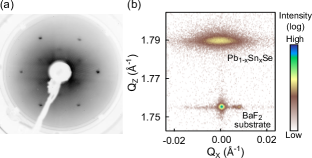
Structural characterization of the grown layers is summarized in Figure 1. Crucially for the present study, low energy electron diffraction (Fig. 1a) consistently exhibits a (111) pattern, indicating that the grown films have assumed the orientation of the BaF2 substrate. A representative sample grown from the source was selected for more comprehensive characterization, including reciprocal space mapping using Cu K X-rays and a high resolution diffractometer, as shown in Figure 1b. Symmetrical reciprocal space maps of the 111 reflection for both the substrate (lower feature) and layer (upper feature) are shown. The grown layer exhibits a higher mosaicity than the substrate, with an angular spread reaching a full width at half maximum of approximately 0.5°. The shape of the upper pattern demonstrates a well defined lattice constant (6.08 Å) which can be mapped to a molar fraction of Szczerbakow1994 . Additional reciprocal space maps (not shown here) of the 115 asymmetric reflection indicate that the grown layer is not strained at room temperature.
Quantitative composition analysis by energy dispersive X-ray spectroscopy (EDX) indicates a Sn content of , laterally uniform throughout the film and in good agreement with the value calculated from reciprocal space mapping. This is higher than the source material () but is still suitable for the observation of a band-inverted condition Dziawa2012 . We note that in this temperature range evaporation occurs molecularly as PbSe and SnSe Springholz2007 . Consequently, while the higher vapor pressure of SnSe compared to PbSe may result in small differences between the chemical composition of the source and the grown layer, reasonable preservation of the source composition is possible with a simple, single source evaporation method.
Taken together, the characterization studies demonstrate that epitaxial, compositionally uniform (111) oriented Pb1-xSnxSe films were produced by this growth method, with a Sn content appropriate for the existence of topological surface states. This is essential for the validation of ARPES measurements, which we now discuss.
III Photoemission measurements
The film growth was performed on the I4 beam line at the MAX-III synchrotron facility Jensen1997 , allowing for extensive ARPES characterization without leaving UHV. All spectra were acquired with linearly p-polarized photons at a sample temperature of 100 K. The photoelectron analyzer was configured for an energy resolution of 25 meV and angular resolution of . Fermi level positions were referenced to a tantalum foil in electrical contact with the samples.
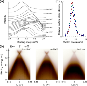
The key result of this study is the observation of surface states with Dirac-like dispersion, occurring at the and the positions in the SBZ. Before studying these states in detail, we first provide confirmation that they are indeed surface states. In Figure 2 we show the results of photon energy dependent ARPES measurements. For the state seen at normal emission, such a measurement probes the - high symmetry direction in the bulk Brillouin zone. Normal emission energy dispersion curves (Figure 2a) show a broad dispersive peak (attributed to the bulk band) together with a sharper, dispersionless peak at a binding energy of 70 meV. The lack of perpendicular dispersion is more clearly apparent in the parallel momentum resolved spectra shown in Figure 2b, and combined with its position within a bulk bandgap serves to confirm that this second peak originates from a surface state.
While the position of the surface state is unchanged when varying the photon energy, the intensity of the state is strongly modulated. The highest intensity is observed at approximately eV; the bulk-state dispersion shown in Figure 2a suggests that this energy probes the valence band maximum. In Figure 2c we illustrate this modulation more clearly by plotting the intensity ratio of the surface state to the bulk band. Similar intensity modulations were observed at approximately 68 eV and 148 eV. Periodic modulation of photoemission intensity with photon energy is a common observation for surface states Bartynski1985 ; Hofmann2002 ; Miwa2013 , with an accepted explanation in terms of a resonant enhancement of the coupling between initial and final states in the photoexcitation process Louie1980 . The enhancement is strongest for perpendicular momenta which minimize the energy separation between the surface state and bulk band it derives from. In the present case, this implies resonance peaks at photon energies which probe the bulk valence band maxima at points. A similar resonant enhancement was observed for the surface state, which while significantly weaker than the state was most intense at a photon energy of 24 eV.
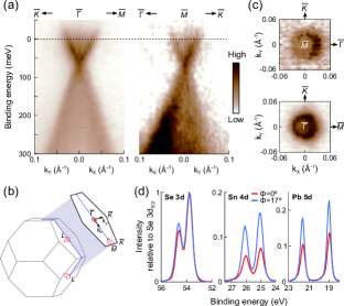
Figure 3 shows energy-momentum ARPES spectra acquired through () and (). Both spectra were measured on a sample grown from Pb0.76Sn0.24Se source material, from which the highest quality data was obtained. Although the composition was not characterized for this sample, there was no observable difference in the band structure compared to samples grown from the Pb0.73Sn0.27Se source, suggesting a similar composition. Figure 3a shows slight anisotropy in the surface state dispersion, with faster dispersion along the cut compared to the cut. In contrast, the state at is isotropic. This can be understood by noting that these surface states derive from the anisotropic bulk bands at the -points, which are projected onto the (111) surface Brillouin zone (Figure 3b). The - direction cuts through the long axis of the bulk constant energy ellipsoids at , giving rise to a slower dispersion. The anisotropy is far less severe than that anticipated for SnTe and Pb0.4Sn0.6Te Safaei2013 ; Liu2013 , and at the Fermi level is barely noticeable (Figure 3c). This is consistent with the reduced eccentricity of the Fermi ellipsoids in PbSe compared to PbTe Svane2010 and is reproduced by the tight binding calculations we will discuss shortly. The Dirac points in Figure 3a are positioned at a binding energy of 70 meV, a value found to be similar across all sample preparations. As anticipated for a (111) surface with cationic termination, the Dirac points sit close to the bulk valence band maxima. Angle dependent core level spectroscopy (Figure 3d) provide supporting evidence that the surface is indeed rich in Sn and Pb cations. Within the experimental resolution, no relative binding energy difference can be observed between the and Dirac points. This is again quite different to calculations for telluride materials, for which the Dirac point is predicted to be 30 meV (Pb0.4Sn0.6Te)Safaei2013 to 45 meV (SnTe)Liu2013 higher in binding energy than the Dirac point. We highlight that differences in Dirac point binding energies are highly relevant for the interpretation of low-energy transport measurements Taskin2013 .
IV Band structure calculations
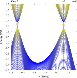
To further investigate our experimental characterization of the (111) surface states (in particular the surface state dispersion anisotropy and Dirac point energy positions), we have performed tight-binding (TB) calculations for a (111) oriented cation terminated slab consisting of 451 layers (80 nm thick). We have used the virtual crystal approximation for the solid solution of PbSe and SnSe, both in rock-salt structure, using temperature-dependent tight binding parameters described previously Wojek2013 . We note that the band structure of rock-salt SnSe has not been verified experimentally, and hence the parameterization of this material is based solely on the results of density functional theory calculations. Despite this, the qualitative aspects of the band structure are well captured Wojek2013 .
As shown in Figure 4, the band calculations for Pb0.64Sn0.36Se at 100 K indicate an inverted bandstructure with Dirac-like surface states at and . Both the dispersion anisotropy and the difference between the and Dirac-point binding energies are in agreement with the experimental ARPES spectra in Figure 3. The qualitative differences we observe in the surface state properties relative to predictions for (Pb,Sn)Te materials can therefore be anticipated purely from the differences between telluride and selenide bulk properties.
V Conclusions
By growing (111) oriented Pb1-xSnxSe films in-situ at a synchrotron ARPES facility, we have been able to spectroscopically measure the topological crystalline insulator states unique to this surface orientation. In contrast to the (100) facet, the Dirac-like surface states are well separated and non-interacting, located at the time reversal invariant momenta and in the surface Brillouin zone. Our observations are captured by a tight binding model, and provide experimental support for the existing body of theoretical work studying the role of surface orientations in TCI materials. Finally, our demonstration of successfully growing and measuring (Pb,Sn)Se films constitutes an important step towards future studies, enabling investigations into the role of strain Barone2013 (through lattice-mismatch from different substrates), additional surface orientations (for example the (110) facet) and atomic step density through substrate vicinality.
Note: Immediately prior to the submission of this work we became aware of a preprint performing a similar study on (111) oriented SnTe Tanaka2013_2 .
Acknowledgements.
This work was made possible through support from the Knut and Alice Wallenberg Foundation, the Swedish Research Council, the European Commission Network SemiSpinNet (PITN-GA-2008-215368), the European Regional Development Fund through the Innovative Economy Grant (No. POIG.01.01.02-00-108/09), and the Polish National Science Centre (NCN) Grant No. 2011/03/B/ST3/02659. P.D. and B. J. K. acknowledge support from the Baltic Science Link project coordinated by the Swedish Research Council, VR. We thank Jacek Osiecki for creating data analysis software used in this study.References
- [1] D. Hsieh, D. Qian, L. Wray, Y. Xia, Y.S. Hor, R.J. Cava, and M.Z. Hasan, Nature 452, 970 (2008)
- [2] Y. Ando, J. Phys. Soc. Jpn. 82, 102001 (2013)
- [3] L. Fu, Phys. Rev. Lett. 106, 106802 (2011)
- [4] T.H. Hsieh, H. Lin, J. Liu, W. Duan, A. Bansil, and L. Fu, Nat. Commun. 3, 982 (2012)
- [5] P. Dziawa, B.J. Kowalski, K. Dybko, R. Buczko, A. Szczerbakow, M. Szot, E. Łusakowska, T. Balasubramanian, B.M. Wojek, M.H. Berntsen, O. Tjernberg, and T. Story, Nat. Mater. 11, 1023 (2012)
- [6] B. M. Wojek, R. Buczko, S. Safaei, P. Dziawa, B. J. Kowalski, M. H. Berntsen, T. Balasubramanian, M. Leandersson, A. Szczerbakow, P. Kacman, T. Story, and O. Tjernberg, Phys. Rev. B 87, 115106 (2013)
- [7] A. Gyenis, I. K. Drozdov, S. Nadj-Perge, O. B. Jeong, J. Seo, I. Pletikosic, T. Valla, G. D. Gu and A. Yazdani, Phys. Rev. B 88, 125414 (2013)
- [8] Y. Okada, M. Serbyn, H. Lin, D. Walkup, W. Zhou, C. Dhital, M. Neupane, S. Xu, Y. J. Wang, R. Sankar, F. Chou, A. Bansil, M. Z. Hasan, S. D. Wilson, L. Fu and V. Madhavan, Science 341, 1496 (2013)
- [9] S.-Y. Xu, C. Liu, N. Alidoust, M. Neupane, D. Qian, I. Belopolski, J.D. Denlinger, Y.J. Wang, H. Lin, L.A. Wray, G. Landolt, B. Slomski, J.H. Dil, A. Marcinkova, E. Morosan, Q. Gibson, R. Sankar, F.C. Chou, R.J. Cava, A. Bansil, and M.Z. Hasan, Nat. Commun. 3, 1192 (2012)
- [10] Y. Tanaka, T. Sato, K. Nakayama, S. Souma, T. Takahashi, Z. Ren, M. Novak, K. Segawa, and Y. Ando, Phys. Rev. B. 87, 155105 (2013)
- [11] Y. Tanaka, Z. Ren, T. Sato, K. Nakayama, S. Souma, T. Takahashi, K. Segawa, and Y. Ando, Nature Phys. 8, 800 (2012)
- [12] M. Safdar, Q. Wang, M. Mirza, Z. Wang, K. Xu, and J. He, Nano Lett. 13, 5344 (2013)
- [13] J. Liu, W. Duan, and L. Fu, arXiv 1304.0430v1 (2013)
- [14] S. Safaei, P. Kacman, and R. Buczko, Phys. Rev. B 88, 045305 (2013)
- [15] A. Lopez-Otero, Thin Solid Films 49, 3 (1978).
- [16] A. Szczerbakow, and H. Berger, J. Crystal Growth 139, 172 (1994)
- [17] G. Springholz and G. Bauer, Phys. Stat. Sol. (B) 244, 2752 (2007)
- [18] B. N. Jensen, S. M. Butorin, T. Kaurila, R. Nyholm, and L. I. Johansson, Nucl. Instr. Meth. Phys. Res. A 394, 243 (1997)
- [19] A. Svane, N. E. Christensen, M. Cardona, A. N. Chantis, M. van Schilfgaarde, and T. Kotani, Phys. Rev. B 81, 245120 (2010)
- [20] A. A. Taskin, S. Sasaki, K. Segawa, and Y. Ando, arXiv 1305.2470v1 (2013)
- [21] R. A. Bartynski, E. Jensen, T. Gustafsson, and E. W. Plummer, Phys. Rev. B 32 1921 (1985)
- [22] Ph. Hofmann, Ch. Søndergaard, S. Agergaard, S. V. Hoffmann, J. E. Gayone, G. Zampieri, S. Lizzit, and A. Baraldi, Phys. Rev. B 66, 245422 (2002)
- [23] J. A. Miwa, P. Hofmann, M. Y. Simmons, and J. W. Wells, Phys. Rev. Lett. 110, 136801 (2013)
- [24] S.G. Louie, P. Thiry, R. Pinchaux, Y. Petroff, D. Chandesris, and J. Lecante, Phys. Rev. Lett. 44, 549 (1980)
- [25] P. Barone, D. Di Sante, and S. Picozzi, Phys. Status Solidi RRL 7, 1102 (2013)
- [26] Y. Tanaka, T. Shoman, K. Nakayama, S. Souma, T. Sato, T. Takahashi, M. Novak, K. Segawa and Y. Ando, arXiv 1312.2803v1 (2013)