Balanced double-loop mesoscopic interferometer based on Josephson proximity nanojunctions
Abstract
We report on the fabrication and characterization of a two-terminal mesoscopic interferometer based on three V/Cu/V Josephson junctions having nanoscale cross-section. The junctions have been arranged in a double-ring geometry realized by metallic thin film deposition through a suspended mask defined by electron beam lithography. Although a significant amount of asymmetry between the critical current of each junction is observed we show that the interferometer is able to suppress the supercurrent to a level lower than 6 parts per thousand, being here limited by measurement resolution. The present nano-device is suitable for low-temperature magnetometric and gradiometric measurements over the micrometric scale.
pacs:
85.35.-p, 85.25.Cp, 85.25.Dq, 74.45.+cTransport properties of hybrid superconductor-normal metal structures at the mesoscopic scale are understood in terms of the proximity effectTaddei, Giazotto, and Fazio (2005); Pannetier and Courtois (2000); Belzig et al. (1999); McMillan (1968a, b); Giazotto et al. (2010), which consists in the modification of the electronic properties of a normal metal in clean contact with a superconductor. Dissipationless transport can be established in superconductor-normal metal-superconductor (SNS) junctions owing to the phase-dependent weak coupling across the diffusive normal metal channel, which can persist over micrometric length scale. The current to phase relationship is sinusoidal in the limit of weak links much longer than the superconducting coherence length 111, where is the diffusion coefficient in the normal metal and is the superconducting energy gap at the leads., so that SNS weak links are functionally equivalent to superconductor-insulator-superconductor (SIS) Josephson junctionsJosephson (1962), featuring however negligible capacitance and much lower typical values of normal-state resistanceLikharev (1979).
Several experimental works concerning superconducting interferometers based on SNS technology have been published recentlyWölbing et al. (2013); Ronzani et al. (2013); Nagel et al. (2011); Angers et al. (2008). One commonly encountered practical issue is that the fabrication protocols do not allow to fully control the quality of the SN interfaces. This results in non-negligible asymmetries in the magnitude of supercurrents between nominally-identical SNS junctions, therefore severely limiting the sensitivity of the interferometer. Here we propose the adoption of a double-loop SNS interferometer configuration as a means to compensate for such asymmetries. This geometry has been proved successful in SIS systems in balancing devices intended for metrologicalKemppinen et al. (2008), quantum computationChiarello et al. (2008) as well as sensingDhong et al. (1983); Sharafiev et al. (2012) applications. Yet, it has been proposed to fully suppress phase-coherent heat currents in caloritronic devicesMartínez-Pérez and Giazotto (2013). With our approach we demonstrate the feasibility of balancing a mesoscopic SNS interferometer to obtain supercurrent suppression ratio values well below one percent, making it an attractive device element for superconducting quantum circuitry and nanoscale sensing applications.

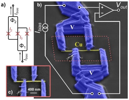
The geometry of a double-loop SNS interferometer consists in the parallel circuit of three Josephson junctions; this configuration defines two superconducting rings, each of which is coupled to a separate magnetic flux [Fig. 1a)]. Figure 1b) shows a scanning electron micrograph of our implementation of this type of interferometer, fabricated by standard electron beam lithography on a suspended bilayer resist maskDolan (1977) (1000 nm copolymer / 100 nm polymethyl-metacrylate) on top of an oxidized silicon substrate. A 5 nm-thick adhesivant aluminium layer has been deposited at via electron-beam evaporation in ultra-high vacuum conditions (), followed by 25 nm of copper at normal incidence; finally, the superconducting leads have been realized by evaporating vanadium in two steps at opposing angles (), 80 nm per step. Excess metal and resist have been removed by lift-off, then the sample has been inspected by scanning electron microscopy and finally wire-bonded to a ceramic dual-in-line chip carrier. The fabricated interferometer features three weak links [Fig. 1c)] consisting of a diffusive normal-metal wire having width and thickness of 45 and 25 nm, respectively; the inter-electrode spacing between vanadium leads is approximately equal to 450 nm. Since the transverse extent of the copper wire is less than the superconducting coherence length , at each vanadium electrode the local222That is, within distance comparable to from the interface with the superconductor. electronic density of states in the normal metal is expected to have a minigap close to the superconducting energy gap in the electrode itself, so that the system can be pictured as having three independent weak linksPfeffer et al. (2013).
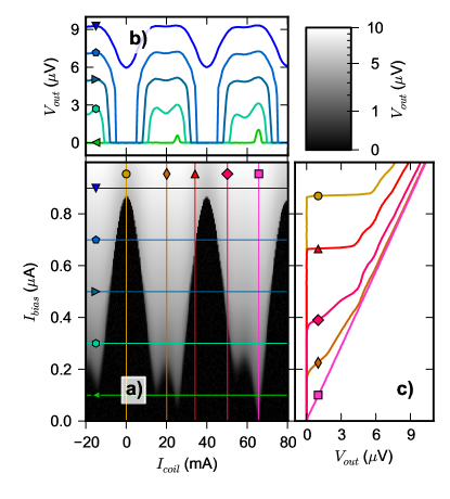
The electron transport properties of the interferometer have been characterized in a filtered cryostat down to . Current vs voltage curves have been recorded by measuring the response to a DC current bias chopped at a reference frequency () using a lock-in amplifier (NF Corp. model LI-5640). The voltage response of the interferometer has been characterized as a function of the current feeding into the superconducting coil used to generate a magnetic field orthogonally to the substrate of the sample, and for several temperatures in the range . Figure 2a) shows the characterization of the interferometer at base temperature (); the typical input referred voltage noise for this setup has been measured to be . The device shows a remarkably linear voltage response for , the characteristic marked with a pink square in Fig. 2c), corresponding to a measured resistance . Additionally, not exactly periodic modulation can be appreciated from the voltage vs flux characteristics shown in Fig. 2b), indicating a slight asymmetry in the effective areas of the two superconducting loops.

The behavior displayed by the device can be understood in terms of a compact model: assuming a sinusoidal current-phase relationship for each Josephson junction and imposing flux quantizationDoll and Näbauer (1961); Deaver and Fairbank (1961) constraints one obtains for the total supercurrent flowing through the interferometer
| (1) |
where is the flux quantum; and respectively represent the critical current and phase difference values for the three Josephson junctions, referring to the central, left and right weak link.
Within this model, the superconducting interferometer is able to conduct a dissipationless current whose maximum value is a function of the magnetic flux values and linked to each superconducting loop. The value of for fixed flux biasing is thus
| (2) |
A key point is that the critical current of the interferometer is given by the magnitude of the vector sum of the critical currents of the three Josephson junctions, with and playing the role of angular displacements between the current vectors representing the lateral junctions with respect to the central one. As such, one can in principle achieve perfect critical current suppression at appropriate values as long as satisfy the triangle inequality:
| (3) |
where are the normalized critical currents of the lateral junctions.
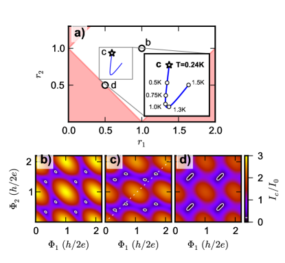
Examples of interferometers having variable degrees of asymmetry can be appreciated in the representation shown in Fig. 3a). The most symmetric case, labeled with the letter b, corresponds to an interferometer in which the three junctions have identical critical current values (); the corresponding map is shown as a color plot in Fig. 3b) and reaches maximum values . A reduced symmetry is represented by the case in which the lateral junctions have identical critical current values, but differ from the central junction (e.g., , labeled as d); Figure 3d) shows the corresponding map. Finally, the generic asymmetric case is represented by , , values which have been found to approximate the behaviour of the presented device at temperature K; this case is labeled with the letter c, and its dependence is presented in Fig. 3c). All three cases fulfill Eqns. 3, showing exact supercurrent suppression for appropriate , values.
In our setup, magnetic flux biasing is provided by an external homogeneous magnetic field 333Proportionality coefficient , so that the flux values and are proportional to the external field and can differ only as a consequence of asymmetry in the effective area values of the superconducting loops:
| (4) |
where is the average loop effective area, is the average magnetic flux bias value and is the effective area asymmetry coefficient.

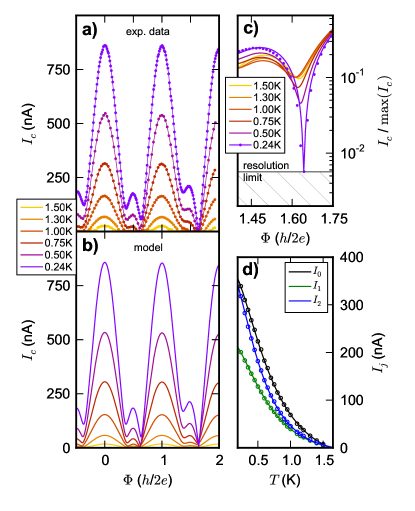
A quantitative analysis of the transport properties of the interferometer has been performed by extracting the values by fitting differential resistance data with a sigmoid test function. This a posteriori approach provides us with switching current data [shown for selected temperature values in Fig. 4a)] which are associated with an uncertainty derived from the quadrature propagation of the intrinsic sigmoid width and the current bias discretization error. At low temperature, the switching is sharp and the relative uncertainty of the extraction process is limited by the latter term (); by increasing temperature the “intrinsic” sigmoid width gradually takes over, reaching typical values of tens of nA at .

The extracted data have been fitted [Fig. 4b)] using Eqns. 2, 4 as a model, estimating a loop surface asymmetry . A direct comparison between data points and model [Figs. 4a,b)] demonstrates the effectiveness of the model in describing our mesoscopic SNS interferometer, particularly impressive considering the minimal amount of hypotheses on which it is based. The fitting procedure provides a quantitative estimate for the temperature dependence of the critical currents of the three constituent Josephson junctions, shown in Fig. 4d). The three junctions show markedly different , both in terms of the characteristic temperature scale of the supercurrent suppression (dependent on the Thouless energy , where is the diffusion coefficient and is the length of the diffusive weak link) and of the magnitude of the supercurrent (affected both by and the transparency of the SN interface). A quantitative modelDubos et al. (2001), whose validity in the high temperature regime () has been experimentally verified for V/Cu/V junctionsGarcia and Giazotto (2009), maps the critical current for a long diffusive SNS weak link to:
| (5) |
with and , where is Boltzmann’s constant, is the elementary charge, is the average normal state resistance of a single junction of the presented device as extracted from current vs voltage measurements, accounts for non-ideality of the normal-superconductor interface and is the superconducting gap at the electrodes, whose temperature dependence has been assumed to be BCS-like (parametrically determined by specifying an effective critical temperature for the vanadium electrodes). This model has been used to fit data for each junction obtaining the parameter estimates reported in Tab. 1. Even though the interferometer has been designed to be symmetric, deviations from ideality inherent to the fabrication process resulted in junctions with quantitatively different and values.
| (eV) | (K) | ||
|---|---|---|---|
| 0.211 0.002 | 15.1 0.2 | 1.61 0.01 | |
| 0.132 0.003 | 13.7 0.4 | 1.66 0.03 | |
| 0.265 0.004 | 10.2 0.2 | 1.68 0.03 |
The presence of measurably different Thouless energy scales introduces a temperature dependence in the parameters for the presented device, as it can be appreciated in the inset of Fig. 3a). Nevertheless, under optimal flux biasing we were able to measure supercurrent suppression values lower than at base temperature [Fig. 4c)], thus confirming the fitness of the double-loop geometry as a means to circumvent junction asymmetry in mesoscopic SNS-based devices.
Finally, it is worth noting that the additional degree of freedom granted by the second loop in our geometry entails the possibility of having the interferometer respond both to the homogeneous part and to the first spatial derivative of the magnetic field (proportional to the sum and difference of and , respectively) on a micrometric length scale; moreover, the relative strength of response can be tuned by designing the interferometer with sensible parameter values444For example, selectively gradiometric response capability is evident in the asymmetric interferometer whose is depicted in Fig. 3d)., easily allowed by the flexibility of the shadow-mask lithographic technique.
The authors acknowledge the Italian Ministry of Defense through the PNRM project “TERASUPER”, the Marie Curie Initial Training Action (ITN) Q-NET 264034 for partial financial support. C.A. thanks the Tuscany Region for funding his fellowship via the CNR joint project “PROXMAG”. A.R. thanks Fondazione Tronchetti Provera for funding his Ph.D. scholarship in Scuola Normale Superiore.
References
- Taddei, Giazotto, and Fazio (2005) F. Taddei, F. Giazotto, and R. Fazio, Journal of Computational and Theoretical Nanoscience 2, 329 (2005).
- Pannetier and Courtois (2000) B. Pannetier and H. Courtois, Journal of Low Temperature Physics 118, 599 (2000).
- Belzig et al. (1999) W. Belzig, F. K. Wilhelm, C. Bruder, G. Schön, and A. D. Zaikin, Superlattices and Microstructures 25, 1251 (1999).
- McMillan (1968a) W. McMillan, Physical Review 175, 537 (1968a).
- McMillan (1968b) W. McMillan, Physical Review 175, 559 (1968b).
- Giazotto et al. (2010) F. Giazotto, J. T. Peltonen, M. Meschke, and J. P. Pekola, Nature Physics 6, 254 (2010).
- Note (1) , where is the diffusion coefficient in the normal metal and is the superconducting energy gap at the leads.
- Josephson (1962) B. Josephson, Physics Letters 1, 251 (1962).
- Likharev (1979) K. Likharev, Reviews of Modern Physics 51, 101 (1979).
- Wölbing et al. (2013) R. Wölbing, J. Nagel, T. Schwarz, O. Kieler, T. Weimann, J. Kohlmann, A. B. Zorin, M. Kemmler, R. Kleiner, and D. Koelle, Applied Physics Letters 102, 192601 (2013).
- Ronzani et al. (2013) A. Ronzani, M. Baillergeau, C. Altimiras, and F. Giazotto, Applied Physics Letters 103, 052603 (2013).
- Nagel et al. (2011) J. Nagel, O. F. Kieler, T. Weimann, R. Wölbing, J. Kohlmann, A. B. Zorin, R. Kleiner, D. Koelle, and M. Kemmler, Applied Physics Letters 99, 032506 (2011).
- Angers et al. (2008) L. Angers, F. Chiodi, G. Montambaux, M. Ferrier, S. Guéron, H. Bouchiat, and J. Cuevas, Physical Review B 77, 165408 (2008).
- Kemppinen et al. (2008) A. Kemppinen, A. J. Manninen, M. Möttönen, J. J. Vartiainen, J. T. Peltonen, and J. P. Pekola, Applied Physics Letters 92, 052110 (2008).
- Chiarello et al. (2008) F. Chiarello, M. G. Castellano, G. Torrioli, S. Poletto, C. Cosmelli, P. Carelli, D. V. Balashov, M. I. Khabipov, and A. B. Zorin, Applied Physics Letters 93, 042504 (2008).
- Dhong et al. (1983) S. H. Dhong, R. E. Jewett, J. W. Spargo, and T. Van Duzer, Journal of Applied Physics 54, 445 (1983).
- Sharafiev et al. (2012) A. Sharafiev, I. Soloviev, V. Kornev, M. Schmelz, R. Stolz, V. Zakosarenko, S. Anders, and H. G. Meyer, Superconductor Science and Technology 25, 045001 (2012).
- Martínez-Pérez and Giazotto (2013) M. J. Martínez-Pérez and F. Giazotto, Applied Physics Letters 102, 092602 (2013).
- Dolan (1977) G. J. Dolan, Applied Physics Letters 31, 337 (1977).
- Note (2) That is, within distance comparable to from the interface with the superconductor.
- Pfeffer et al. (2013) A. Pfeffer, J. E. Duvauchelle, H. Courtois, R. Mélin, D. Feinberg, and F. Lefloch, (2013), arXiv:1307.4862 .
- Doll and Näbauer (1961) R. Doll and M. Näbauer, Physical Review Letters 7, 51 (1961).
- Deaver and Fairbank (1961) B. Deaver and W. Fairbank, Physical Review Letters 7, 43 (1961).
- Note (3) Proportionality coefficient .
- Dubos et al. (2001) P. Dubos, H. Courtois, B. Pannetier, F. Wilhelm, A. D. Zaikin, and G. Schön, Physical Review B 63, 064502 (2001).
- Garcia and Giazotto (2009) C. P. Garcia and F. Giazotto, Applied Physics Letters 94, 132508 (2009).
- Note (4) For example, selectively gradiometric response capability is evident in the asymmetric interferometer whose is depicted in Fig. 3d).