Giant thermovoltage in single InAs-nanowire field-effect transistors
Abstract
Millivolt range thermovoltage is demonstrated in single InAs-nanowire based field effect transistors. Thanks to a buried heating scheme, we drive both a large thermal bias and a strong field-effect modulation of electric conductance on the nanostructures. This allows the precise mapping of the evolution of the Seebeck coefficient as a function of the gate-controlled conductivity between room temperature and . Based on these experimental data a novel estimate of the electron mobility is given. This value is compared with the result of standard field-effect based mobility estimates and discussed in relation to the effect of charge traps in the devices.
The quest for large-scale solid-state thermoelectric (TE) conversion was one of the major driving forces behind semiconductor research before the discovery of the transistor effect Majumdar04 . Expectations were not met, however, largely because of efficiency issues and the high costs and material toxicity. Indeed achievement of efficient TE devices requires a non-trivial tuning of interdependent material parameters and can be expressed in terms of the maximization of the figure of merit , where is the Seebeck coefficient, and are the electrical and thermal conductivities, the average operation temperature Majumdar04 ; BookTE . Large values proved elusive over the past decades despite the great design flexibility offered by semiconductor heterostuctured materials Snyder08 . Nanotechnology has recently revived the interest on this research area and may be able to play the role of a game-changer. It enables the design of artificial materials with novel properties and thus opens alternative routes to the optimization of thermodynamic efficiency Dresselhaus07 ; Vineis10 ; Shi12 ; Venkatasubramanian01 ; Boukai08 ; Poudel08 ; Heremans08 . Among these, nanowire-based structures have attracted a significant interest Shi10 ; Martinez11 ; Lee11 ; Zhou11 ; Tian12 ; Moon13 .
In this Letter, we focus on the TE properties of single InAs nanowires (NWs), self-assembled nanostructures actively investigated in view of a number of potential applications in novel electronics RoddaroNR11 ; Spathis11 ; Giazotto11 and optoelectronics Vitiello12 ; Pitanti11 . The present InAs NW model system is also particularly relevant for the investigation of strongly-confined low-dimensional systems ThelanderAPL2003 ; Bjork04 ; Fuhrer07 ; Roddaro11 ; Romeo12 , which in turn may make available exciting heat-transport and TE properties Hoffmann09 ; Zhang11 . Here we demonstrate that record-high thermovoltage values in excess of can be induced in devices comprising a single-NW as active element and that these values can be modulated by field-effect. A buried-heater approach allows us to combine a large thermal gradient with the field-effect control of single nanostructures deposited on standard oxidized silicon. We highlight that this scheme can be of general interest for the investigation of a large class of nanomaterials with potential TE applications. We shall provide a precise map of the Seebeck coefficient in our NWs as a function of from room temperature down to . Also, since vs. curves are strongly dependent on electron scattering times, our experimental data lead to an estimate of the electron mobility , which we shall compare with the values obtained with the standard approach based on field-effect mobility . The role of surface states and gate hysteresis Halpern12 in NW transport properties and in our parameter estimates will be discussed.
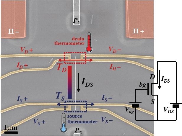
One of the single-NW field-effect transistors (FETs) studied is depicted in Fig. 1. Devices were built starting from -diameter InAs NWs deposited by drop casting over the SiO2/Si substrate. Source (S) and drain (D) electrodes were fabricated at different distances ranging from up to (device in the figure). These contacts could be operated both as electrical leads and resistive thermometers, thanks to their multi-contact arrangement. Consequently we could sample temperatures and at the two ends of the FET and the thermal bias . The four-wire thermometers were operated using a small AC current bias () and a phase-locked measurement technique while the DC transport along the NW was being simultaneously monitored. The doped Si substrate played the dual role of backgate electrode and differential heater. Two current injection leads and were used to establish a non-uniform current density in the substrate portion below the NW. By suitably tuning heater bias we could control both the temperature jump along the wire ( and were measured using the resistive thermometers) and the local backgate potential . Operation details and performance of the present heating scheme will be presented elsewhere, while further information on the devices and the measurement procedures are provided in the Methods and in the Supplementary Material sections.
As shown in Fig. 2a, the IV characteristics of our FETs were always linear within the explored electrical/thermal biasing ranges according to:
| (1) |
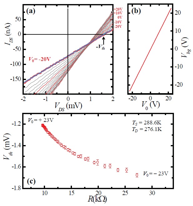
where is the NW resistance and is the thermovoltage due to the NW-Au thermocouple, and are the Seebeck coefficients of the NW and of the electrodes, respectively. Very large thermovoltages beyond were obtained and a strong modulation could be driven by field effect. The FET behavior was measured at temperatures ranging from up to (values were calculated as the average between and ). Differential heating was obtained by applying a heater bias with respect to the device ground contact . This led at the same time to a backgate potential . The gating bias was also directly monitored by probes and in order to correct for any deviations from device symmetry. For every heating configuration (i.e. for a given value) a full backgate scan was performed stepping from to with a relatively slow speed of about . At each gating value, an IV sweep was recorded in alternating directions, along with the back-gate voltage value . Figure 2a shows the IV curves measured for the device in Fig. 1 with which yielded and . The correspondence between and the backgate voltage is shown in Fig. 2b: for this value , the small difference being linked to the resistance drops at the contacts. From these data we can readily calculate thermovoltage and resistive slope . Figure 2c shows the resulting evolution of thermovoltage versus resistance .
Thanks to the direct measurement of temperatures and and to the large attainable, a rather precise mapping of was determined for over 20 temperature values between and and for ranging from a minimum of to a maximum of . Figure 3a reports some of the curves obtained. Note that the small contribution due to was subtracted using , a good approximation in the explored temperature regime Mott . In addition, was calculated as , where is the known series resistance of the measurement set-up (contact resistances are negligible with respect to ) and . The hexagonal NW section was calculated as , given is the corner-to-corner “diameter” that was measured by scanning electron microscopy. The corresponding power factor is plotted in Fig.3b and peaks on the high-conductivity side of the graph. We also note that displays a monotonic dependence on for every given value of with an almost linear dependence on . This is directly visible in Fig. 3c where values show a good overlap and the slight sublinearity of vs becomes evident.
The overall evolution of the NW Seebeck coeffiecient can be understood starting from the approximate law
| (2) |
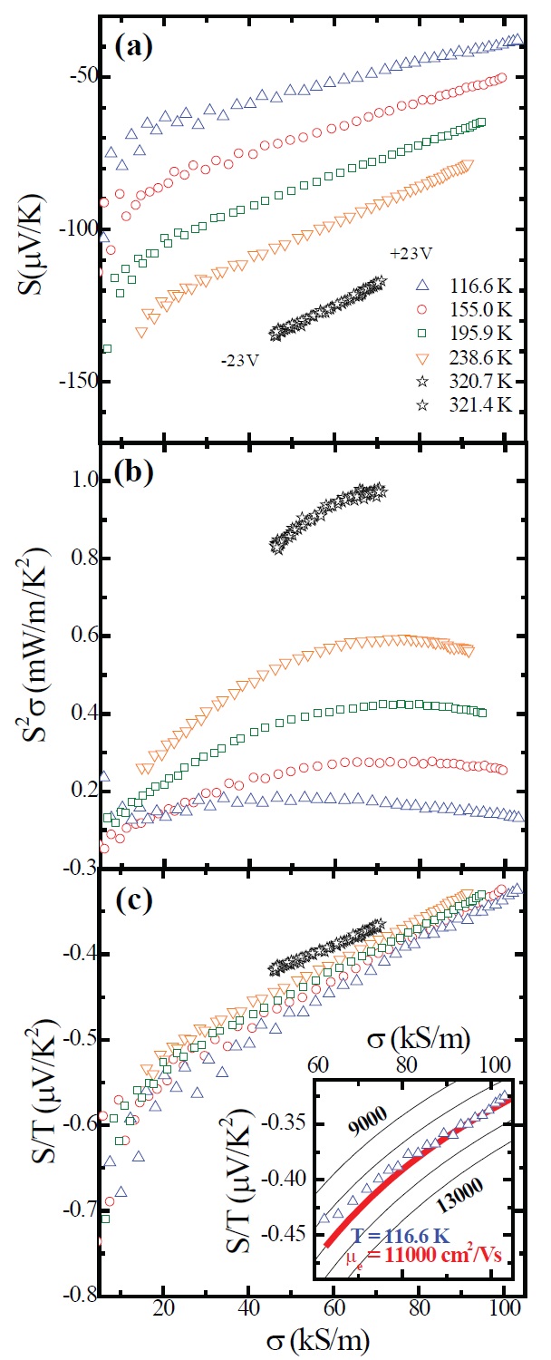
which is valid for degenerate semiconductors in the low limit note02 ; Mott . Assuming that the temperature dependence of the mobility is small, this approximation would imply that is temperature-independent: data in Fig. 3c indicate that such expectation is almost exactly valid in the present case. We compare the model with the lowest temperature dataset () in the high band-filling regime (i.e. for large ’s), which is the one we expect to best comply with the model approximations. Since the mobility is the only free parameter of the model (see Supplementary Materials), this leads to an interesting estimate, with respect to the more standard one derived from field-effect in transport. In the inset to Fig. 3c we compare experimental data with predictions for an energy-independent , using no further adjustable parameters. A rather good agreement is obtained for . Note that since the prediction is sensitive to the density of states, it is important to stress that only a minor non-parabolicity can be expected at the corresponding band filling (along the visible red part of the curve, to from the -point band edge).
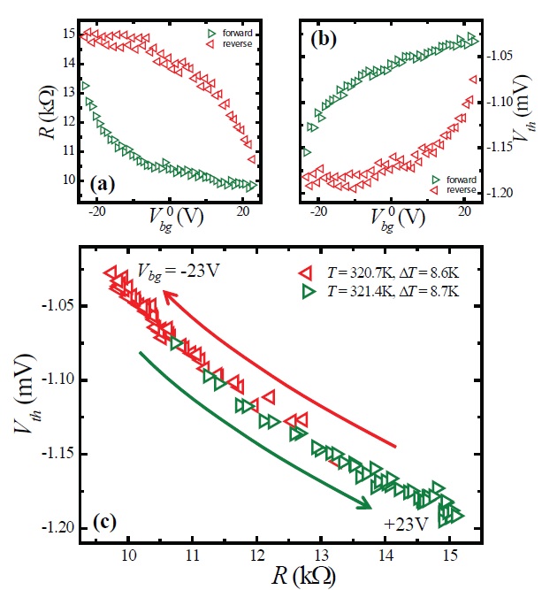
Albeit this is an approximate fit and lower conductivity data would require at least to take quantum confinement and finite temperature effects into account, the present estimate is robust and very instructive. In fact this value can be directly compared with , which we can determine in parallel starting from the dependence of the NW transconductance (see Supplementary Materials). This procedure was observed to lead to values lower than , for all explored and regimes in the same NW. Such a sizable underestimate of field-effect mobility with respect to our fit procedure is robust despite the relatively strong approximation of energy-independent , since it is consistently observed across all explored filling regimes in the NWs, almost down to the pinch-off. This discrepancy was never directly measured but was discussed independently in recent works, where it was pointed out that estimates of the NW free-carrier density values obtained by field effect are usually significantly overestimated as a consequence of surface-charge screening effects Blomers12 ; Storm12 and non-ideal aspects of the gating geometry Pitanti12 . In turn, this typically leads to a systematic underestimate of the carrier mobility. In this sense, the transport analysis discussed in Fig. 3 provides novel insight since it is largely independent from the influence of surface states. This is demonstrated by analyzing data in Fig. 4. Let us first examine (panel (a)) and (panel (b)) and compare data taken in the two opposite sweep directions at with and . No further parameter is modified during the measurement. A significant hysteresis is present in the dependence: this behavior is a consequence of the slow dynamics of surface states and traps, leading to a time-dependent screening of the gate Roddaro08 ; Karlstrom08 . Remarkably, despite the very large history-dependence of both and as a function of , the parametric trajectory in the - space is largely unaffected by sweep direction as shown Fig. 4(c). This confirms nicely that even if hysteresis affects the free-charge filling of the NW as a function of , it has a negligible effect on the other transport parameters such as the carrier mobility .
In conclusion, we demonstrated that large thermovoltages can be induced and tuned by gating in single-NW transistors. This result was obtained with a buried-heater scheme that makes it possible to impose both a large thermal bias and electric gating to the nanostructure. This experimental arrangement yielded a detailed mapping of that was compared with classic models for thermoelectric transport in degenerate semiconductors. The adopted approximations led to a alternative estimate of electron mobility in the NW. This value is significantly larger than the one obtain by field-effect, , on the same wire. The discrepancy can be understood in terms of the influence of slow surface- and trap-charge dynamics on field-effect mobility measurements, an influence that was shown to be negligible on vs. dependence. The present results indicate that special care must be taken in the interpretation of transport results based on field-effects in these nanostructures.
Acknowledgements. We gratefully acknowledge G. Signore for support with chemical passivation of the NWs. The work was partly supported by the Marie Curie Initial Training Action (ITN) Q-NET 264034 and by MIUR through the PRIN2009 project “Dispositivi ad effetto di campo basati su nanofili e superconduttori ad alta temperatura critica”. SS acknowledges the support of the Academy of Finland, project NANoS (project number 260815).
Methods. InAs NWs were grown by metal assisted chemical beam epitaxy in a Riber C-21 reactor, using tertiarybutylarsine (TBAs) and trimetylindium (TMIn) as metalorganic precursors for group V and group III elements with line pressures of 3.00 and 0.90 Torr, respectively. Ditertiarybutylselenide (DtBSe) with a line pressure of 0.30 Torr was used as n-doping source. Devices were built starting from -diameter InAs NWs deposited by drop casting over a SiO2/Si substrate. The substrate was heavily doped, with a resistivity , and was covered by a -thick oxide. In a first lithographic step aligned to the NW, heater contacts ( and in Fig. 1) and the backgate voltage probes ( and ) were defined by etching the SiO2 layer and depositing a Ni/Au (/) bilayer on the exposed Si. In the second step, the thermometers and all connections to the bonding pads were defined by a single evaporation of a Ti/Au / bilayer. Prior to evaporation the NW contact regions were exposed to an solution to passivate the surface and avoid the formation of an insulating oxide layer Suyatin . The device was operated in a chamber containing a small amount of exchange gas (He), inside a variable-temperature cryostat. The sample holder was equipped with a calibrated Si-diode thermometer which was used to measure the bath temperature and calibrate the two resistive thermometers at the and contacts. Details about the heater operation and about the precise thermal and electrical calibration procedures adopted for the experiments are reported in the Supplementary Materials.
References
- (1) A. Majumbdar, Thermoelectricity in Semiconductor Nanostrucutres, Science 303, 777 (2004).
- (2) G. S. Nolas, J. Sharp, H. J. Goldsmid, Thermoelectrics: Basic Principles and New Materials Developments, Springer New York, 2001.
- (3) G. J. Snyder, and E. S. Toberer, Complex thermoelectric materials, Nature Mat. 7, 105 (2008).
- (4) M. S. Dresselhaus, G. Chen, M. Y. Tang, R. Yang, H. Lee, D. Wang, Z. Ren, J.-P. Fleurial, and P. Gogna, New Directions for Low-Dimensional Thermoelectric Materials, Adv. Mat. 19, 1043 (2007).
- (5) C. J. Vineis, A. Shakouri, A. Majumdar, and M. G. Kantzidis, Nanostructured Thermoelectrics: Big Efficiency Gains from Small Features, Adv. Mat. 22, 3970 (2010).
- (6) L. Shi, Thermal and Thermoelectric Transport in Nanostructures and Low-Dimensional Systems, Nanoscale and Microscale Thermophysical Engineering 16, 79 (2012).
- (7) R. Venkatasubramanian, E. Siivola, T. Colpitts and B. O’Quinn, Thin-film thermoelectric devices with high room-temperature figures of merit, Nature 413, 597 (2001).
- (8) A. I. Boukai, Y. Bunimovich, J. Tahir-Kheli, J.-K. Yu, W. A. Goddard III, and J. R. Heath, Silicon nanowires as effcient thermoelectric materials, Nature 451, 06458 (2008).
- (9) B. Poudel, Q. Hao, Y. Ma, Y. Lan, A. Minnich, B. Yu, X. Yan, D. Wang, A. Muto, D. Vashee, X. Chen, J. Liu, M. S. Dresselhaus, G. Chen, and Z. Ren, High-Thermeolectric Performance of Nanostructured Bismuth Antimony Telluride Bulk Alloys, Science 320, 634 (2008)
- (10) J. P. Heremans, V. Jovovic, E. S. Toberer, A. Saramat, K. Kurosaki, A. Charoenphkdee, S. Yamanaka, and G. S. Snyder, Enhancement of Thermoelectric Efficiency in PbTe by Distortion of the Electronic Density of States, Science 321, 554 (2008).
- (11) L. Shi, D. Yao, G. Zhang, and B. Li, Large thermoelectric figure of merit in Si1-xGex nanowires, Appl. Phys. Lett. 96, 173108 (2010).
- (12) J. A. Martinez, P. P. Provencio, S. T. Picraux, J. P. Sullivan, and B. S. Swartzentruber, Enhanced thermoelectric figure of meriti in SiGe alloy nanowires by boundary and hole-phonon scattering, J. Appl. Phys. 110, 074317 (2011).
- (13) , S. H. Lee, W. Shim, S. Y. Jang, J. W. Roh, P. Kim, J. Park, and W. Lee, Thermeoelctric properties of inidividual single-crystalline PbTe nanowires grown by a vapour transport method, Nanotech. 22, 295707 (2011).
- (14) F. Zhou, A. L. Moore, J. Bolinsson, A. Persson, L. Fröberg, M. T. Pettes, H. Kong, L. Rabenberg, P. Caroff, D. A. Stewart, N. Mingo, K. A. Dick, L. Samuelson, H. Linke, and L. Shi, Thermal conductivity of indium arsenide nanowires with wurtzite and zinc blende phases, Phys. Rev. B 83, 205416 (2011).
- (15) Y. Tian, M. R. Sakr, J. M. Kinder, D. Liang, M. J. MacDonald, R. L. J. Qiu, H.-J. Gao, and X. P. A. Gao, One-Dimensional Quantum Confinement Effect Modulated Thermoelectric Properties in InAs Nanowires, Nano Lett. 12, 6492 (2012).
- (16) J. Moon, J.-H. Kim, Z. C. Y. Chen, J. Xiang, R. Chen, Gate-Modulated Thermoelectric Power Factor of Hole Gas in Ge-Si Core-Shell Nanowires, Nano Lett. 13, 1196 (2013).
- (17) S. Roddaro, A. Pescaglini, D. Ercolani, L. Sorba, F. Giazotto, and F. Beltram, Hot-electron Effects in InAs Nanowire Josephson Junctions, Nano Res. 4, 259 (2011).
- (18) P. Spathis, S. Biswas, S. Roddaro, L. Sorba, F. Giazotto, and F. Beltram, Hybrid InAs nanowire-vanadium proximity SQUID, Nanotech. 22, 105201 (2011).
- (19) F. Giazotto, P. Spathis, S. Roddaro, S. Biswas, F. Taddei, M. Governale, and L. Sorba, A Josephson quantum electron pump, Nature Phys. 7, 857 (2011).
- (20) M. S. Vitiello, D. Coquillat, L. Viti, D. Ercolani, F. Teppe, A. Pitanti, F. Beltram, L. Sorba, W. Knap, and A. Tredicucci, Room-Temperature Terahertz Detectors Based on Semiconductor Nanowire Field-Effect Transistors Nano Lett. 12, 96 (2012).
- (21) A. Pitanti, D. Ercolani, L. Sorba, S. Roddaro, F. Beltram, L. Nasi, G. Salviati, and A. Tredicucci, InAs/InP/InSb Nanowires as Low Capacitance n-n Heterojunction Diodes Phys. Rev. X 1, 011006 (2011).
- (22) C. Thelander, T. Mårtensson, M. T. Björk, B. J. Ohlsson, M. W. Larsson, L. R. Wallenberg, and L. Samuelson, Single-electron transistors in heterostructure nanowires, Appl.Phys.Lett. 83, 2052 (2003).
- (23) M. T. Björk, C. Thelander, A. E. Hansem, L. E. Jensen, M. W. Larsson, L. R. Wallenberg, and L. Samuelson, Few-Electron Quantum Dots in Nanowires, Nano Lett. 4, 1621 (2004).
- (24) A. Fuhrer, L. E. Fröberg, J. N. Pedersen, M. W. Wallenberg, A. Wacker, M.-E. Pistol, and L. Samuelson, Few-Electron Double Dots in InAs/InP Nnaowire Heterostrucutres, Nano Lett. 7, 243 (2007).
- (25) S. Roddaro, A. Pescaglini, D. Ercolani, L. Sorba, and F. Beltram, Manipulation of Electron Orbitals in Hard-Wall InAs/InP Nanowire Quantum Dots, Nano Lett. 11, 1695 (2011).
- (26) L. Romeo, S. Roddaro, A. Pitanti, D. Ercolani, L. Sorba, and F. Beltram, Electrostatic Spin Control in InAs/InP Nanowire Quantum Dots, Nano Lett. 12, 4490 (2012).
- (27) E. A. Hoffmann, H. A. Nilsson, J. E. Matthews, N. Nakpathomkun, A. I. Persson, L. Samuelson, and H. Linke, Measuring Temperature Gradients over Nanometer Length Scales, Nano Lett. 9, 779 (2009).
- (28) Y. Zhang, M. S. Dresselhaus, Y. Shi, Z. Ren, and G. Chen, High Thermoelectric Figure-of-Merit in Kondo Insulator Nanowires at Low Temperatures Nano Lett. 11, 1166 (2011).
- (29) E. Halpern, G.Elias, A. V. Kretinin, H. Shtrikman, and Y. Rosenwaks, Direct measurement of surface states density and energy distribution in individual InAs nanowires, Appl. Phys. Lett. 100, 262105 (2012).
- (30) N. F. Mott and H. Jones, The Theory of the Properties of Metals and Alloys, Courier Dover Publications, 1985.
- (31) The expected energy spacing between the one-dimensional subbands can be calculated to be for our wires, the adoption of a three-dimensional band dispersion relation provides an acceptable description of the nanowire at such high carrier densities.
- (32) Ch. Blömers, T.Grap, M. I. Lepsa, J. Moers, St. Trellenkamp, D. Grützmacher, H. Lüth, and Th. Schäpers, Hall effect measurement on InAs nanowires, Appl. Phys. Lett. 101, 152106 (2012).
- (33) K. Storm, F. Halvardsson, M. Heurlin, D. Lingren, A. Gustafsson, P. M. Wu, B. Monemar, and L. Samuelson, Spatially resolved Hall effect measurement in a single semiconductor nanowire, Nature Nanotech. 7, 718 (2012).
- (34) A. Pitanti, S. Roddaro, M.S.Vitiello, and A.Tredicucci, Contacts shiedling in nanowire field effect transistors J. Appl. Phys. 111, 064301 (2012).
- (35) S. Roddaro, K. Nilsson, G. Astromskas, L. Samuelson, L.-E. Wernersson, O. Karlström, and A. Wacker, InAs nanowire metal-oxide-semiconductor capacitors, Appl. Phys. Lett. 92, 253509 (2008).
- (36) O. Karlström, A. Wacker, K. Nilsson, G. Astromskas, S. Roddaro, L. Samuelson and L.-E. Wernersson, , Analysing the capacitance-voltage measurements of vertical wrapped-gated nanowires, Nanotech. 19, 435201 (2008).
- (37) D. B. Suyatin, C. Thelander, M. T. Björk, I. Maximov, and L. Samuelson, Sulfur passivation for ohmic contact formation to InAs nanowires, Phys. Rev. B 44, 1646 (1991).