Thermionic charge transport in CMOS nano-transistors
Abstract
We report on DC and microwave electrical transport measurements in silicon-on-insulator CMOS nano-transistors at low and room temperature. At low source-drain voltage, the DC current and RF response show signs of conductance quantization. We attribute this to Coulomb blockade resulting from barriers formed at the spacer-gate interfaces. We show that at high bias transport occurs thermionically over the highest barrier: Transconductance traces obtained from microwave scattering-parameter measurements at liquid helium and room temperature is accurately fitted by a thermionic model. From the fits we deduce the ratio of gate capacitance and quantum capacitance, as well as the electron temperature.
Recent CMOS technology allows for the fabrication of silicon-on-insulator structures of nano-metric size. Depending on fabrication strategy, charge transport in these devices can be quasi-zero- or one-dimensional: Field-effect devices based on narrow silicon channels with spacer regions surrounding the gate can exhibit single-electron-transistor (SET) characteristics Hofheinz et al. (2006); Roche et al. (2012); Shin et al. (2011), whereas gate-all-arround nanowires formed in Si fins show 1D behavior, e.g. conductance quantization due to subband formation Colinge and Xiong (2006); Yi et al. (2011); Razavieh
et al. (2013a).
Silicon nanowires on silicon-on-insulator (SOI) substrates have recently been shown to be promising candidates for future low-power and radio frequency (RF) applications Barraud et al. (2012); Grenouillet et al. (2012); Razavieh
et al. (2013a, b). The linearity of the RF response is improved due to the one-dimensional, ballistic charge transport in such devices and the possibility to operate them in the so called quantum capacitance limit, where the gate voltage controls mainly the bands or levels in the transistor channel.
Whether these requirements for RF linearity can also be met in devices that predominantly exhibit SET-like behaviour has not been studied extensively yet.
This letter presents a study of the nature of electron transport in narrow channel CMOS silicon field-effect devices at low and high bias. They consist of a narrow Si channel in silicon-on-insulator substrate with a local top-gate and global back-gate. Spacer elements separate the source and drain electrodes from the top-gate, which in conjunction with surface roughness and remote charges in the gate stack induces two barriers in the potential landscape Voisin et al. (2013). We show that at low temperature and low bias electron transport is governed by Coulomb blockade due to these barriers, observable directly e.g. in the source-drain current as a function of bias and top-gate voltage at temperature.
From microwave scattering-parameter measurements at low temperature we determine a different impact of the barriers depending on source-drain voltage: At low bias both barriers contribute, whereas at high bias transport occurs quasi-thermionically and only the highest of both barriers plays a role. Using a thermionic transport model we are able to reproduce the device’s transconductance and deduce the ratio of total capacitance and quantum capacitance as well as the electron temperature. Further microwave measurements show that the devices operate in the hot electron regime at high bias up to room temperature.
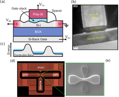
Devices were fabricated in fully depleted SOI substrate at LETI facilities. First the active regions were patterned by etching the SOI layer above the buried oxide (BOX) forming undoped Si channels of thickness . After short oxidation of the channel () the gate stack is formed ( HfSiON, TiN and poly-Si) and etched (see Fig.1(e)). Silicon nitride spacers of length were deposited on both sides of the gate and the source-drain contacts raised by epitaxial growth of Si (). Both source and drain were then highly doped by extension implantation and activation annealing. Fig.1(a) and (b) show a sketch and a TEM micrograph of a typical device. Similar to Roche et al. (2012), the devices have a non-overlap profile due to the spacers. The doping gradient under the spacers together with surface roughness and remote charges in the gate stack induce potential barriers as sketched in Fig.1(c). In a last step the devices were silicided (NiPtSi). All devices presented in this letter are embedded in a adapted coplanar wave guide for RF measurements (see Fig.1(d)). Gate lengths and channel widths of devices present in this letter are shown in Table I.
| device | device | ||||
|---|---|---|---|---|---|
| RFM2-1 | 44 | 10 | RFM4-3a | 64 | 30 |
| RFM1-2 | 44 | 30 | RFM4-3b | 64 | 30 |
| RFM1-4 | 64 | 10 | RFM3-1 | 114 | 10 |
DC and RF probe station measurements were carried out at room temperature and liquid helium temperature in a Janis variable temperature probe station.
The RF response was probed with a vector network analyzer at frequencies GHz: After a short-open-load-through calibration, we obtained the scattering parameters for each pair of gate voltages and converted them to admittance parameters Pallecchi et al. (2011). The conversion is favourable since parasitic, parallel elements can then simply be subtracted Pozar (2005). We use the device’s off-state as dummy signal and obtain the de-embedded admittance , where is the threshold voltage, the top-gate and the back-gate voltage. Note that in the following the subscript DUT is omitted and refers to the de-embedded admittance signal. DC traces are recorded simultaneously with the RF measurements.
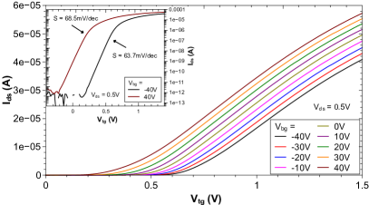
In Fig.2 we present first of all the DC current of device RFM1-2 (, ) at as a function of top-gate voltage for various back-gate voltages. The device shows a good transistor behavior with off-state current in the region for and a subtreshold slope - (see Fig.2), close to the theoretical limit of for thermally activated transport at Sze (1981). Here, is the Boltzmann constant and the electron charge. As previously reported by Roche et al. (2012), the threshold voltage shifts with back-gate voltage.
We turn now to characterizing the nature of charge transport in our devices. As described in the introduction of this letter, charge transport through a narrow silicon channel can in general occur via one-dimensional channels Razavieh
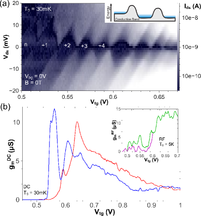
et al. (2013a) or through the levels of a single-electron-transistor-like structure Roche et al. (2012). In order to discriminate between the two mechanisms, we have carried out DC measurements in a dilution fridge setup at and RF probe station measurements at . Fig.3(a) is a colorscale plot of the current in sample RFM1-4 just below the turn-on voltage of the transistor at . Clear Coulomb diamonds are visible, indicating the presence of two barriers and subsequent conductance quantization as depicted in Fig.1(c) and the inset to Fig.3(a).
Fig.3(b) shows the transconductance of devices RFM4-3, RFM3-1 and RFM2-1 at low bias and and , respectively. The DC transconductance is calculated from the DC current as . At RF it can directly be read from the forward admittance as . Similar to the device of Fig.3(a), RFM4-3a and RFM4-3b show Coulomb blockade at low with a charging energy of about (not shown here). The DC transconductance reflects this, as can be seen from the oscillations of at in Fig.3(b). In addition, the DC transconductance remains flat below threshold. Above threshold we observe two peaks and a steady decline thereafter. The RF counterparts of RFM3-1 and RFM2-1 were obtained at and and , respectively. Consequently these traces exhibit several peaks below threshold as function of with a gate spacing of - for RFM2-1 (purple). For the device of longest gate length, RFM3-1 (green), peaks below threshold are less pronounced, but prevail beyond threshold, similar to of devices RFM4-3a and b. We attribute the additional small variations, e.g. at , to increased disorder in the device. Overall, we infer that low bias transport is governed by barriers formed at the spacer-gate interfaces. Their effect manifests in both DC and RF measurements.
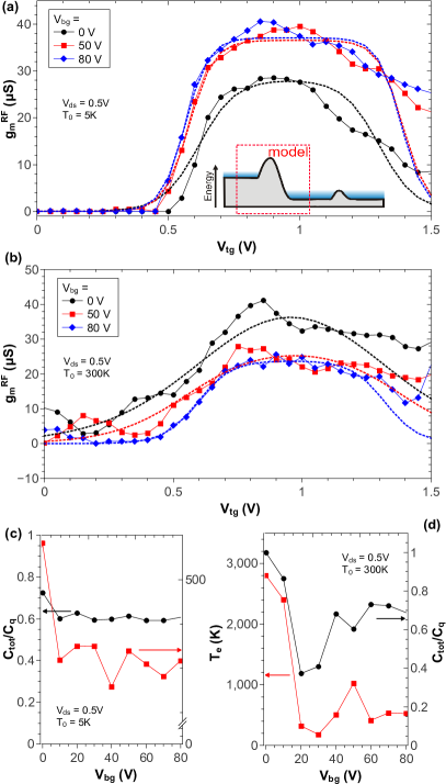
The picture changes when the source-drain bias is raised to higher values: Fig.4(a) shows the transconductance extracted from low temperature RF scattering-parameter measurements in device RFM2-1. Contrary to the low bias case of Fig.3(b), now shows only one broad peak as function of . Owing to the high , i.e. large potential drop between source and drain, transport is now dominated by only one barrier and we can fit data by a simple 1D nanotransistor model, as outlined in Chaste et al. (2010). Here, the transistor is described as a 1D channel with one classical barrier between the leads. A corresponding potential landscape is shown as inset of Fig.4(a). The model takes into account a potential as highlighted in red. Only electrons with energies high enough to clear the barrier contribute to the charge transport in this model. Transport over the barrier is thus thermionic and one can derive the corresponding transconductance Chaste et al. (2010)
| (1) |
where . and are the total gate and the quantum capacitance John et al. (2004), respectively; is an additional factor accounting for residual diffusive charge transport over the barrier. The contacts are modelled by the Fermi distributions and , where is the electron temperature. All three parameters, , and , depend on source-drain voltage and back-gate bias. Assuming that the barrier height is controlled by , i.e. , as well as Chaste et al. (2010) and using , , as fitting parameters, we obtain the dashed lines shown in Fig.4(a) and (b). The good agreement between data and fit - performed for each - shows that transport is dominated by only the highest barrier in the high bias regime and can be regarded as quasi one-dimensional.
At low temperature the transconductance peak is more pronounced than at room temperature and we find from the fits that the device works in the hot electron regime: The electron temperature , shown in Fig.4(c) as function of , is much higher than the substrate temperature . Fig4(c) also presents the extracted ratio of total gate to quantum capacitance. On average , i.e. . The device hence operates in between the classical, charge controlled limit () and the quantum capacitance limit () Razavieh
et al. (2013b). Similar to the RF transconductance, one can obtain the total gate capacitance from RF Y-parameter measurements as . We find - for - . Residual diffusive transport remains moderate with an average ”ballisticity” factor (not shown here). At room temperature, we obtain a noisier RF response and thus larger uncertainty in the fitting procedure. Data can still be modelled by Eq.1, i.e. transport is still thermionic. On average, the electron temperature remains at a similar level as in the low temperature measurements (see Fig.4(d)), as does the capacitance ratio . Residual diffusive transport however increases at room temperature and we now obtain on average (not shown here).
In conclusion, we have studied the nature of charge transport at low and high bias in narrow channel SOI field-effect devices. We show that at low bias transport is governed by barriers emerging in the undoped region under the spacer elements, whereas at high bias transport occurs quasi-one-dimensional over the highest barrier. In the latter case the device’s behaviour can be described with a thermionic transport theory and we accurately model the device transconductance. The devices operate in the thermionic transport regime from liquid helium to room temperature.
The authors thank D.A. Williams and A.J. Ferguson for fruitful discussion. The research leading to these results has been supported by the European Community’s seventh Framework under the Grant Agreement No. 318397. The samples presented in this work were designed and fabricated by the TOLOP project partners, http://www.tolop.eu.
References
- Hofheinz et al. (2006) M. Hofheinz, X. Jehl, M. Sanquer, G. Molas, M. Vinet, and S. Deleonibus, Applied Physics Letters 89, 143504 (2006).
- Roche et al. (2012) B. Roche, B. Voisin, X. Jehl, R. Wacquez, M. Sanquer, M. Vinet, V. Deshpande, and B. Previtali, Applied Physics Letters 100, 032107 (2012).
- Shin et al. (2011) S. J. Shin, J. J. Lee, H. J. Kang, J. B. Choi, S.-R. E. Yang, Y. Takahashi, and D. G. Hasko, Nano Letters 11, 1591 (2011).
- Colinge and Xiong (2006) J. Colinge and W. Xiong, IEEE Electron Device Letters, IEEE 27, 775 (2006).
- Yi et al. (2011) K. S. Yi, K. Trivedi, H. C. Floresca, H. Yuk, W. Hu, and M. J. Kim, Nano letters 11, 5465 (2011).
- Razavieh et al. (2013a) A. Razavieh, S. Mehrotra, N. Singh, G. Klimeck, D. Janes, and J. Appenzeller, Nano Letters 13, 1549 (2013a).
- Barraud et al. (2012) S. Barraud, R. Coquand, M. Casse, M. Koyama, J.-M. Hartmann, V. Maffini-Alvaro, C. Comboroure, C. Vizioz, F. Aussenac, O. Faynot, et al., IEEE Electron Device Letters 33, 1526 (2012).
- Grenouillet et al. (2012) L. Grenouillet, M. Vinet, J. Gimbert, B. Giraud, J. P. Noel, Q. Liu, P. Khare, M. A. Jaud, Y. Le Tiec, R. Wacquez, et al., in 2012 International Electron Devices Meeting (IEEE, 2012), pp. 3.6.1–3.6.4.
- Razavieh et al. (2013b) A. Razavieh, D. B. Janes, and J. Appenzeller, IEEE Transactions on Electron Devices 60, 2071 (2013b).
- Voisin et al. (2013) V.-H. Voisin, B. andNguyen, J. Renard, X. Jehl, S. Barraud, F. Triozon, M. Vinet, I. Duchemin, Y.-M. Niquet, S. de Franceschi, and M. Sanquer (2013), in preparation.
- Pallecchi et al. (2011) E. Pallecchi, C. Benz, A. C. Betz, H. V. Löhneysen, B. Plaçais, and R. Danneau, Applied Physics Letters 99, 113502 (2011).
- Pozar (2005) D. M. Pozar, Microwave Engineering (John Wiley and sons, 2005), 3rd ed.
- Sze (1981) S. M. Sze, Physics of semiconductor devices (John Wiley and sons, 1981), 2nd ed.
- Chaste et al. (2010) J. Chaste, E. Pallecchi, P. Morfin, G. Fève, T. Kontos, J.-M. Berroir, P. Hakonen, and B. Plaçais, Applied Physics Letters 96, 192103 (2010).
- John et al. (2004) D. L. John, L. C. Castro, and D. L. Pulfrey, Journal of Applied Physics 96, 5180 (2004).