Broadband nanoelectromechanical phase shifting of light on a chip
Abstract
We demonstrate an optomechanical phase shifter. By electrostatically deflecting the nanofabricated mechanical structure, the effective index of a nearby waveguide is changed and the resulting phase shift is measured using an integrated Mach-Zehnder interferometer. Comparing to thermo-optical phase shifters, our device does not consume power in static operation and also it can operate over large frequency, wavelength, and power ranges. Operation in the MHz range and sub-s pulses are demonstrated.
Integrated on-chip optics has many advantages over free-space optics, such as compactness, scalability, and stability. This is especially important for quantum computation with light Knill et al. (2001). We envision a structure with on-chip sources of correlated photons Davanco et al. (2012); Jiang et al. (2012); Laucht et al. (2012), that are guided through nanophotonic structures implementing a quantum-computation algorithm, then storing Fiore et al. (2011) the result in a quantum optomechanical resonator Poot and van der Zant (2012), finally followed by detection with highly efficient integrated superconducting single photon detectors Pernice et al. (2012); Schuck et al. (2013a, b). In such a platform all operations are performed on a single chip, reducing coupling losses, enhancing the device stability, and making the entire system easily scalable.

Phase shifters are an essential part for the quantum information processing with photons as well as for other applications. These are devices that can controllably change the phase of the light field. When a photon travels a length through a material with a refractive index , the phase that it acquires is , where is the free-space wavelength. Since the path length is difficult to change in an integrated optical circuit, phase shifts are induced by changing the refractive index. Current on-chip phase modulators use different techniques to achieve this: First of all, one can change the effective refractive index of a waveguide by injecting carriers into it Xu et al. (2005); Reed et al. (2010). This technology is widely used in the semiconductor and photonic industry, but cannot be used with important insulating materials such as SiN. Another commonly used way to phase-modulate light on a chip is to use the temperature dependence of the refractive index: by placing a heater close to the waveguide, the refractive index can be modulated Vlasov et al. (2005); Pruessner et al. (2007); Beggs et al. (2010). However, this technique typically requires a large power to be dissipated on the chip Song et al. (2008) making it challenging to implement at the cryogenic temperatures required for superconducting detectors. Furthermore, even at room temperature, thermal crosstalk between closely spaced thermo-optical devices is a severe problem. Other designs for phase modulators have employed movable parts to change the resonant wavelength of an on-chip cavity Winger et al. (2011); Sun et al. (2012); Miao et al. (2012); Sridaran and Bhave (2011); Abdulla et al. (2011). However, all these devices are intrinsically narrowband in nature, either to the wavelength of the input light, or to the modulation frequency when resonant modulation is required.
Here we demonstrate broadband on-chip phase shifting of near-infrared light by electrostatically actuating a nanomechanical structure that is placed in the vicinity of an optical waveguide. The device (Fig. 1(a)-(c)) consists of SiN photonic circuits and a mechanical resonator that can be displaced by applying a voltage between two electrodes. The in-plane deflection modifies the effective refractive index of the waveguide, thereby phase-shifting the light traveling through it Guo et al. (2012). By integrating the waveguide in one of the arms of a Mach-Zehnder interferometer (MZI) this phase shift is detected. Note again that our devices do not rely on light within a narrow wavelength range in contrast to cavity-based systems: In principle, the operation wavelength is only limited by the bandwidth of the waveguides used (the cut-off wavelength of the waveguide is around 1800 nm), but in our current implementation the wavelength range is set by the transmission window of the grating couplers spanning up to 50 nm in the telecom wavelength range.
The mechanical part of the device shown in Fig. 1(a)-(c) consists of four SiN arms with width and length . One side of the arms is fixed at the clamping points and the other side is connected to a block at the center of the resonator, forming an “H” (Fig. 1). An electrode runs over one pair of arms and is separated from a second, fixed, electrode by a small gap . There is also a narrow gap between the remaining two arms and the waveguide. To facilitate the release and in order to prevent leakage of light from the waveguide into the block, holes are etched in the block forming a photonic crystal with a bandgap around the operating wavelength yet retaining the rigidity of the block. Still, the most important point of our “H-resonator” design is that the electrodes are far away from the waveguide thus avoiding absorption of the light in the metal Davanço et al. (2012).
The phase shifters are made on a silicon handle substrate with oxide (cladding) and a thick (device) layer of high-stress SiN ( and stress ) on top. The devices are fabricated in a three-step electron beam lithography process, followed by a wet release. The electrodes (5 nm Cr and 210 Au) are patterned first. Then the couplers and waveguides are written and dry-etched. The nitride is not completely etched: a thin () layer of SiN remains on the silicon oxide to protect the latter during the wet release. Next, the moveable structures are defined and etched all the way through the SiN. Both etching steps are aligned w.r.t. the electrodes using metal alignment markers defined in the first step. Note that the last lithography step has to be aligned within this small gap between the electrodes. Typically, the alignment between all layers is better than 40 nm.
The effect of the in-plane motion of the mechanical structure on the propagation through the waveguide is calculated with two-dimensional finite-element (FEM) simulations in COMSOL. Figure 1(d) shows the dependence of the effective refractive index of the first TE-like mode on the separation between the 1000-nm-wide waveguide and the arms of the resonator. Without the resonator (i.e., for ) is 1.450 but increases to 1.462 at . Thus by displacing the resonator the phase acquired by the light traveling through the upper arm can be controlled. The total phase shift accumulated over the entire interaction length of the device (i.e., the length over which the waveguide runs close to the resonator; is the length of the whole device) is then:
| (1) |
where is the average in-plane displacement along the arms closest to the waveguide. To attain the largest phase shifts the derivative has to be as large as possible and hence should be as small as possible. Devices with between 125 and 225 nm and and 225 nm have been fabricated; for narrower gaps the devices tend to stick to either the waveguide or the fixed electrode. The capacitance between the electrodes depends strongly on as shown in Fig. 1(e). By applying a voltage an attractive electrostatic force per unit length results, where is the capacitance per unit length Poot and van der Zant (2012). For a capacitive gap of 225 nm the data in Fig. 1(e) yields a total force of on the resonator at . The mechanical compliance of the structure is mainly determined by the four arms so that the spring constant if the force were localized on the block instead of being distributed along the entire H-resonator. The displacement that is obtained with this simple estimate is 200 nm; a full FEM simulation of the static displacement shows that the block displaces 134 nm towards the electrode and that the average displacement is away from the waveguide. Combining everything shows than the expected phase shift is for a device with .
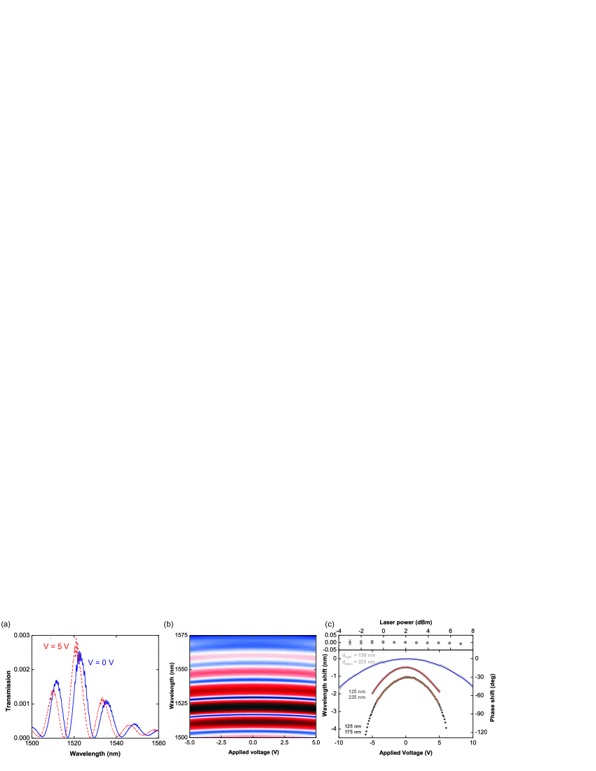
In the experiment, light from a tunable laser source with power is sent from a single mode optical fiber onto the chip using a grating coupler (the triangular structures in Fig. 1(b)) and passed though the MZI which converts the phase shift into an amplitude change. The modulated light is coupled into a second fiber and detected with a photodetector. AC and DC electrical signals are combined with a bias-T and are applied to the device using a high-frequency ground-signal-ground probe. Figure 2(a) shows the optical transmission of the device. MZI fringes with a period of are imprinted on the overall transmission profile of the grating couplers. Now when a voltage is applied, the fringes of the MZI interferometer shift towards shorter wavelengths (Fig. 2(a)). This can be understood as follows: the voltage pulls the resonators away from the waveguide, reducing and thus decreasing the phase accumulated in the (90- longer) upper arm of the MZI. To bring the phase difference back to its original value, a smaller wavelength is needed and hence the fringes shift to the left. Figure 2(b) shows a colormap of the transmission of the device for different applied voltages. For both positive and negative polarities the curves bend downward indicating that the electrostatic force is always attractive Poot and van der Zant (2012). By extracting the position of the fringes, the tuning curves shown in Fig. 2(c) are obtained. As discussed above, devices with smaller gaps and are expected to have the largest wavelength shifts. Indeed, the fringes of the device with and shift more than 3 nm at -6 V. A quadratic fit of yields a curvature of . This is much larger than the curvature reported in Ref. Sun et al. (2012) and comparable to the narrowband device of Ref. Winger et al. (2011). Using the period of the MZI fringes, the wavelength shift can be converted back to a phase shift. In this case which can be compared to the curvature calculated using Eq. (1) , where . The calculated curvature is a bit higher than the measured one, possibly due to the unknown stress in the metal and the difference between the actual and designed gaps on which the derivatives depend sensitively. In any case, the right axis of Fig. 2(c) shows that a single device generates a phase shift of more than and a full phase shift would be achieved at . Larger phase shifts (or, equivalently, a smaller ) can easily be obtained by cascading multiple H-modulators.
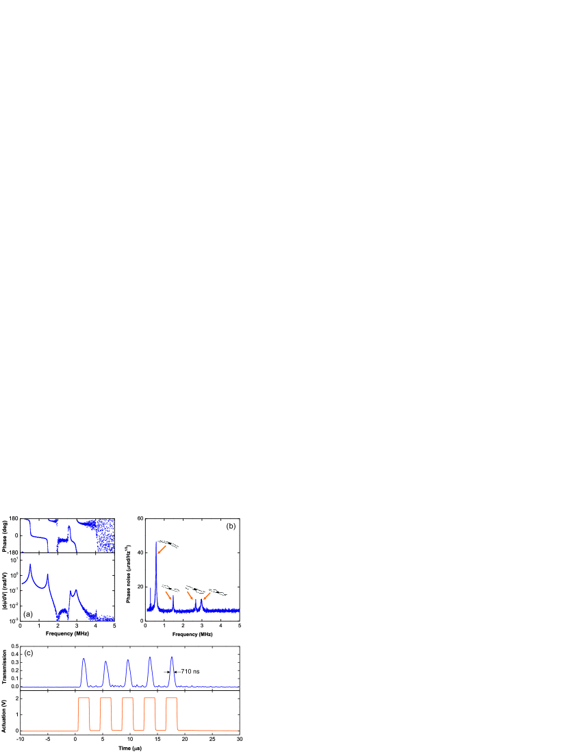
Figure 3(a) shows the dynamic behavior of the device. The output of a network analyzer is added to the static voltage and the response at the excitation frequency is measured. These measurements show that our phase shifter is not only broadband in the optical sense, but operates over a large modulation frequency range: The 3 dB point occurs at 1.0 MHz and coherent operation up to a few MHz is possible before the signal is lost in the noise. The magnitude contains a series of peaks. These are the eigenfrequencies of the H-resonator where the dynamic phase shift is resonantly enhanced by the mechanical quality factor . A flatter frequency response can be engineered by lowering , for example by operating in liquid or by coating with mechanically lossy polymers. Alternatively, one could utilize negative feedback to operate the device at lower quality factors Miao et al. (2012).
By measuring the output of the photodetector with a spectrum analyzer and converting the voltage noise power spectral density back to a phase, the noise spectrum of Fig. 3(b) is obtained. It has a background of which is due to the noise of the laser and of the photodetector; these are thus not intrinsic to the device. However, the peaks are the Brownian motion of the eigenmodes (the peak at 0.27 MHz is, however, due to the laser). At the fundamental mode (at 0.58 MHz) the entire resonator is moving, whereas the higher modes are mainly located on the arms. The noise performance of the phase shifter also can be improved by intentionally reducing the mechanical quality factor.
The device can also generate fast phase shifts as demonstrated in Fig. 3(c). Here, a pulse train of five rectangular pulses is applied Liu et al. (2008) (bottom) resulting in the output signal in the top panel. Due to the high resonance frequency of the H-resonator sub- pulses are realized. The pulse width of is already much shorter than state-of-the-art thermo-optic devices Song et al. (2008); Atabaki et al. (2010), but by engineering the pulse shape, even shorter pulses are possible Harjanne et al. (2004).
Finally, the dynamic range of the optical power is considered. At low optical power , the device does not feel the influence of the light traveling through the waveguide, but at high power the attractive optical gradient force will pull the resonator closer to it. This was actually the operation principle of the devices studied in Ref. Fong et al. (2011) and was for example used to build an optomechanical radio-frequency amplifier Li et al. (2012), but is unwanted for an electrically controlled phase modulator. The gradient force Povinelli et al. (2005) per unit length is where is the speed of light in vacuum. The power in the waveguide that causes the same force as is about 70 mW for the parameters discussed above; for a 10 times higher operation voltage this value changes to 7 W, indicating that in practice the optical power does not play a role. Indeed, in the experiment no change of the fringe position with laser power was observed up to 6.9 dBm (Fig. 2(c)). Besides being broadband in the electrical and optical sense, our optomechanical phase shifter is thus also capable of handling a large range of optical power.
Acknowledgements.
M.P thanks Netherlands Organization for Scientific Research (NWO) / Marie Curie Cofund Action for providing a Rubicon postdoctoral fellowship. This work was partly funded by the DARPA/MTO ORCHID program through a grant from AFOSR. H.X.T. acknowledges support from a Packard Fellowship in Science and Engineering and a career award from National Science Foundation. Facilities used were supported by Yale Institute for Nanoscience and Quantum Engineering and NSF MRSEC DMR 1119826. We thank Wolfram Pernice for discussions.References
- Knill et al. (2001) E. Knill, R. Laflamme, and G. J. Milburn, A scheme for efficient quantum computation with linear optics, Nature 409, 46 (2001).
- Davanco et al. (2012) M. Davanco, J. R. Ong, A. B. Shehata, A. Tosi, I. Agha, S. Assefa, F. Xia, W. M. J. Green, S. Mookherjea, and K. Srinivasan, Telecommunications-band heralded single photons from a silicon nanophotonic chip, Appl. Phys. Lett. 100, 261104 (pages 4) (2012).
- Jiang et al. (2012) W. C. Jiang, X. Lu, J. Zhang, O. Painter, and Q. Lin, A silicon-chip source of bright photon-pair comb, arXiv:1210.4455 (2012).
- Laucht et al. (2012) A. Laucht, S. Pütz, T. Günthner, N. Hauke, R. Saive, S. Frédérick, M. Bichler, M.-C. Amann, A. W. Holleitner, M. Kaniber, et al., A Waveguide-Coupled On-Chip Single-Photon Source, Phys. Rev. X 2, 011014 (2012).
- Fiore et al. (2011) V. Fiore, Y. Yang, M. C. Kuzyk, R. Barbour, L. Tian, and H. Wang, Storing Optical Information as a Mechanical Excitation in a Silica Optomechanical Resonator, Phys. Rev. Lett. 107, 133601 (2011).
- Poot and van der Zant (2012) M. Poot and H. S. J. van der Zant, Mechanical systems in the quantum regime, Phys. Rep. 511, 273 (2012).
- Pernice et al. (2012) W. Pernice, C. Schuck, O. Minaeva, M. Li, G. Goltsman, A. Sergienko, and H. Tang, High-speed and high-efficiency travelling wave single-photon detectors embedded in nanophotonic circuits, Nat Commun 3, 1325 (2012).
- Schuck et al. (2013a) C. Schuck, W. H. Pernice, X. Ma, and H. X. Tang, Optical time domain reflectometry with low noise waveguide-coupled superconducting nanowire single-photon detectors, Appl. Phys. Lett. 102, 191104 (2013a).
- Schuck et al. (2013b) C. Schuck, W. H. P. Pernice, and H. X. Tang, Waveguide integrated low noise NbTiN nanowire single-photon detectors with milli-Hz dark count rate, Sci. Rep. 3, 1 (2013b).
- Xu et al. (2005) Q. F. Xu, B. Schmidt, S. Pradhan, and M. Lipson, Micrometre-scale silicon electro-optic modulator, Nature 435, 325 (2005).
- Reed et al. (2010) G. T. Reed, G. Mashanovich, F. Y. Gardes, and D. J. Thomson, Silicon optical modulators, Nat Photon 4, 518 (2010).
- Vlasov et al. (2005) Y. A. Vlasov, M. O’Boyle, H. F. Hamann, and S. J. McNab, Active control of slow light on a chip with photonic crystal waveguides, Nature 438, 65 (2005).
- Pruessner et al. (2007) M. W. Pruessner, T. H. Stievater, M. S. Ferraro, and W. S. Rabinovich, Thermo-optic tuning and switching in SOI waveguide Fabry-Perot microcavities, Opt. Express 15, 7557 (2007).
- Beggs et al. (2010) D. M. Beggs, T. P. White, T. Kampfrath, K. Kuipers, and T. F. Krauss, Slow-light photonic crystal switches and modulators, Proceedings of SPIE 7606, 76060N (2010).
- Song et al. (2008) J. Song, Q. Fang, S. H. Tao, T. Y. Liow, M. B. Yu, G. Q. Lo, and D. L. Kwong, Fast and low power Michelson interferometer thermo-optical switch on SOI, Opt. Express 16, 15304 (2008).
- Winger et al. (2011) M. Winger, T. D. Blasius, T. P. M. Alegre, A. H. Safavi-Naeini, S. Meenehan, J. Cohen, S. Stobbe, and O. Painter, A chip-scale integrated cavity-electro-optomechanics platform, Opt. Express 19, 24905 (2011).
- Sun et al. (2012) X. Sun, X. Zhang, M. Poot, C. Xiong, and H. X. Tang, A superhigh-frequency optoelectromechanical system based on a slotted photonic crystal cavity, Appl. Phys. Lett. 101, 221116 (pages 5) (2012).
- Miao et al. (2012) H. Miao, K. Srinivasan, and V. Aksyuk, A microelectromechanically controlled cavity optomechanical sensing system, New J. Phys. 14, 075015 (2012).
- Sridaran and Bhave (2011) S. Sridaran and S. A. Bhave, Electrostatic actuation of silicon optomechanical resonators, Opt. Express 19, 9020 (2011).
- Abdulla et al. (2011) S. Abdulla, L. Kauppinen, M. Dijkstra, M. de Boer, E. Berenschot, H. Jansen, R. de Ridder, and G. Krijnen, Tuning a racetrack ring resonator by an integrated dielectric MEMS cantilever, Opt. Express 19, 15864 (2011).
- Guo et al. (2012) X. Guo, C.-L. Zou, X.-F. Ren, F.-W. Sun, and G.-C. Guo, Broadband opto-mechanical phase shifter for photonic integrated circuits, Appl. Phys. Lett. 101, 071114 (2012).
- Davanço et al. (2012) M. Davanço, J. Chan, A. H. Safavi-Naeini, O. Painter, and K. Srinivasan, Slot-mode-coupled optomechanical crystals, Opt. Express 20, 24394 (2012).
- Liu et al. (2008) N. Liu, F. Giesen, M. Belov, J. Losby, J. Moroz, E. A. Fraser, G. McKinnon, J. T. Clement, V. Sauer, K. W. Hiebert, et al., Time-domain control of ultrahigh-frequency nanomechanical systems, Nat Nano 3, 715 (2008).
- Atabaki et al. (2010) A. H. Atabaki, E. S. Hosseini, A. A. Eftekhar, S. Yegnanarayanan, and A. Adibi, Optimization of metallic microheaters for high-speed reconfigurable silicon photonics, Opt. Express 18, 18312 (2010).
- Harjanne et al. (2004) M. Harjanne, M. Kapulainen, T. Aalto, and P. Heimala, Sub-s switching time in silicon-on-insulator Mach-Zehnder thermooptic switch, Photonics Technology Letters, IEEE 16, 2039 (2004).
- Fong et al. (2011) K. Y. Fong, W. H. Pernice, M. Li, and H. X. Tang, Tunable optical coupler controlled by optical gradient forces, Opt. Express 19, 15098 (2011).
- Li et al. (2012) H. Li, Y. Chen, J. Noh, S. Tadesse, and M. Li, Multichannel cavity optomechanics for all-optical amplification of radio frequency signals, Nat Commun 3, 1091 (2012).
- Povinelli et al. (2005) M. L. Povinelli, M. Loncar, M. Ibanescu, E. J. Smythe, S. G. Johnson, F. Capasso, and J. D. Joannopoulos, Evanescent-wave bonding between optical waveguides, Opt. Lett. 30, 3042 (2005).