All electron topological insulator in InAs double wells
Abstract
We show that electrons in ordinary III-V semiconductor double wells with an in-plane modulating periodic potential and inter well spin-orbit interaction are tunable Topological Insulators (TIs). Here the essential TI ingredients, namely, band inversion and the opening of an overall bulk gap in the spectrum arise, respectively, from (i) the combined effect of the double well even-odd state splitting together with the superlattice potential and (ii) the interband Rashba spin-orbit coupling . We corroborate our exact diagonalization results by an analytical nearly-free electron description that allows us to derive an effective Bernevig-Hughes-Zhang (BHZ) model. Interestingly, the gate-tunable mass gap drives a topological phase transition featuring a discontinuous Chern number at meV. Finally, we explicitly verify the bulk-edge correspondence by considering a strip configuration and determining not only the bulk bands in the non-topological and topological phases but also the edge states and their Dirac-like spectrum in the topological phase. The edge electronic densities exhibit peculiar spatial oscillations as they decay away into the bulk. For concreteness, we present our results for InAs-based wells with realistic parameters.
pacs:
73.63.Hs,71.70.Ej,73.40.-cI Introduction
Topological Insulators (TI) have been theoretically predicted in graphene Kane and Mele (2005) and in negative-gap or inverted-band HgTe-based quantum wells Bernevig et al. (2006), being experimentally realized in the latter shortly after König et al. (2007). These are exotic solids being bulk insulators with metallic edges or surfaces hasan-kane ; Qi and Zhang (2011). An essential ingredient for a system to exhibit TI phases is the existence of a tunable bulk band gap that can not only be tuned to zero but also invert its sign. Defining as “positive gap” the case in which it can be mapped without closing onto the gap separating the positive- and negative-energy solutions of the Dirac equation (“vacuum”), one can immediately see that an interface between materials with positive and negative gaps must support gapless (edge or surface) states Pankratov et al. (1987). Time reversal symmetry and spin orbit interaction inextricably lock the spin and momentum of these states making them helical koenig .
More recently, interesting works have proposed TIs with ordinary bulk materials Liu et al. (2008); patrik ; Sushkov and Neto (2013); dong , as naturally occurring inverted-band or negative-gap materials are usually unconventional narrow band-gap systems. These proposals rely on externally inducing a band inversion of the electron and hole states, e.g., electrically in double well systems Liu et al. (2008); knez ; patrik . Hexagonal patterns fabricated in -doped GaAs well to resemble the physics of Dirac carriers in graphene offer another means to attain TI phasesSushkov and Neto (2013). Another appealing idea is the use of built-in polarization fields to induce band inversion and TI phases in Ge sandwiched between GaAs layers dong . All of these works rely on electrons and holes Liu et al. (2008); patrik ; dong or holes only Sushkov and Neto (2013)
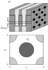
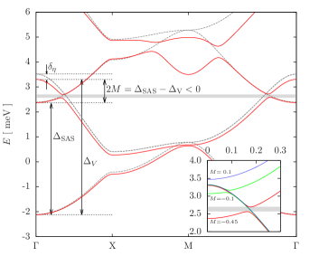
Here we propose a TI based on ordinary III-V semiconductor nanostructures with only electrons. We consider a bilayer quantum well with two confined electron subbands and intersubband spin-orbit coupling (ISOC) Calsaverini et al. (2008); she , Fig. 1a. Such even/odd two band systems have been realized in wide quantum well hernandes . By fabricating a periodic pattern on top of the structure (e.g. via etching) and depositing metal gates gives rise to an in-plane modulating superlattice potential within the QW schlosser , Fig. 1a, we are able to obtain the necessary ingredients for a TI: (i) tunable inverted subbands controlled by the ‘mass gap’ that depends on both the double-well even-odd state splitting and the quantity that is determined by the gate controllable parameters of the periodic potential, and (ii) a bulk overall gap controlled via the ISOC that gives rise to anti crossings, see bands around the -point in Fig. 2. In principle the Fermi energy can be tuned so as to lie in the bulk gap. The sign of can be tuned either through (different quantum well structures) or the gate-controllable , see Appendix A.
We solve the problem within the physically appealing nearly-free electron description. In this approach we analytically derive an effective BHZ model for our system Bernevig et al. (2006). We also solve the problem numerically via exact diagonalization thus determining the full energy spectrum within the Brillouin zone. In the appropriate parameter range the two descriptions agree very well. We also calculate the topological invariant from our bulk band structure and show that the system undergoes a topological phase transition when the mass changes sign, indicated by a discontinuity in the topological invariant as a function of or , see Fig. 4. We then find the solutions for a strip configuration to verify the bulk-edge correspondence explicitly: in the non-topological phase () our system is a bulk insulator with no edge states while in the topological regime () it features, in addition, gapless edge states with Dirac-like bands, see Fig. 5. Interestingly, we find that the edge states display oscillations as they spatially decay away from the border into bulk, see Fig. 6. These oscillations can in principle be mapped via scanning gate microscopy recently used to probe edge states in HgTe-based TI wells koenig .
II Model system
Our effective model describes the two lowest subbands of a symmetric quantum well (plus spin). In the basis of the (e)ven and (o)dd eigenstates we have
| (5) |
where denotes the electron momentum and . Here is the interband spin-orbit coupling Calsaverini et al. (2008) and the electron effective mass. The Hamiltonian in (5) can be put into the standard BHZ form by the unitary transformation acting on each diagonal block. This results in the new upper diagonal block
| (8) |
The lower diagonal block is the time reversed version of Eq. (8): . Equation (8) has a form reminiscent of the diagonal blocks of the BHZ model, apart from the inverted band structure Bernevig et al. (2006). In the BHZ model the inverted band structure arises from the peculiar ordering of bands of HgTe combined with the tunability of the electron and hole levels in a well geometry. Here we will engineer an inverted-band system from the ordinary double well with normal ordering of bands by superimposing a two dimensional superlattice on top of it, Fig. 1a and b. We choose the periodic potential (period ) as
| (9) |
where .
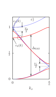
This potential gives rise to parabolic dispersions around the -point with positive curvature (mass) for the first and second subbands and negative curvature for the third band, schematically shown in Fig. 1c. More specifically, the superlattice Hamiltonian is
| (10) |
where we have used . The corresponding eigensolutions are Bloch wave functions with energies , has the same periodicity as kittel95:book . It is convenient to define the energy scale , which for InAs () and, say, superlattice period nm, yields meV.
III Gapped bulk spectrum: Numerics
Figure 2 shows the band structure (red curves) obtained via exact diagonalization using the parameters: meV, meV, meV, and meVnm Calsaverini et al. (2008). The interband coupling can be further increased by optimizing the quantum well structure Li et al. (2008).
The term opens up a gap at the -point, giving rise to a negative curvature band, and facilitates the coupling between the second and third states for finite values, see Eqs. (24) and (25). When the gap opens up over the full Brillouin zone. The gray dashed curves show the bands in the absence of the spin-orbit coupling . The 2nd and 3rd bands clearly show inversion and crossings for , while a non-zero opens up gaps at the crossing (red curves). The energy splitting of the inverted bands is given by the tunable mass gap . The parameter is defined as the energy difference between the 1st and 3rd energy bands at the -point, see Fig. 2. The value of the even-odd energy splitting is controlled by the structure of the quantum well confining potential. The inset in Fig. 2 is a blowup of the band crossing for meV and three different values of , going from an inverted ordering of bands for meV and meV to a normal ordering at meV. The bands in Fig. 2 are doubly degenerate due to the time-reversed part of the full Hamiltonian, i.e. the Kramers pairs.
IV Nearly-free electron description
Here we focus on the 2nd and 3rd bands for (see gray curves in Fig. 2), which comprise the two inverted crossing bands required by the BHZ model. To obtain analytical results and a better qualitative understanding of our system we now follow a perturbative approach based on the nearly free electron model (NFEM).
IV.1 Energy bands and controlled band inversion
We start by looking at the single quantum well in the presence of a periodic potential. Using Bloch’s theorem, the eigenvalue problem corresponding to the Hamiltonian in Eq. (10) reduces to
| (11) | |||||
In the spirit, we are interested in finding the energy spectrum at the -point () and then use these states to calculate the energy bands away from the -point, using pertubation theory to obtain corrections due to . For the free electron model, the energy levels at the -point occur at (1 state), (4 degerate states), (4 degerate states), etc. , where . To describe the inverted bands we need to consider the four normalized states that cross at
| (12) |
and the ground state at , i.e. . The 4 states in Eq. (12) are coupled by the term and using degenerate perturbation theory the new states and corresponding eigenenergies are
| (13) | |||||
| (14) | |||||
| (15) | |||||
| (16) |
and the corresponding eigenergies are , , , and . The state , that gets lowered in energy by , along with the ground state that we denote by (eigenenergy ) will form the inverted bands when the even/odd state energy separation in the bilayer system is considered.
Anticipating the energy spectrum for the bilayer system we simplify the notation and use the same labeling scheme as in Fig. 1c) and denote state 2A in Eq. (13) by and corresponding eigenenergy . The second order perturbation theory correction to states and at are
| (17) | |||||
| (18) | |||||
The quantity related to the superlattice potential that enters into the mass gap is the bandwidth , which is defined as the difference between the top of the second band and the bottom of the first band:
| (19) |
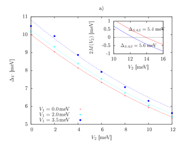
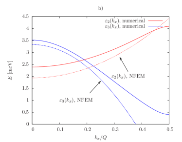
The NFEM calculation, along with full numerics, of the bandwidth are plotted as a function of , for three values of in Figure 3a). In the range corresponding to the values used in the paper the behavior of is predominantly linear in with second order corrections contributing to higher values of and .
An intuitive way, although not mathematically rigorous, to understand why the nearly-free electron model gives qualitatively good results, even for , is to write the periodic potential in terms of Fourier components
which shows that the coupling constants entering the pertubative calculations are effectively and , i.e. smaller than , even for as we use in the manuscript.
For simplicity we exhibit the bands along the direction and suppress the varible for clarity. Next we show that the curvature of is negative. Lowest order perturbation in results in
| (20) | |||||
which shows that the curvature is indeed negative for values of kittel95:book ; ashcroft . In our calculations we use yielding , which compares well to the numerical value of , extracted by fitting the full numerics with a parabolic dispersion. The other band that will form the inverted band structure is , which is the same as apart from a shift in energy of . The curvature of is simply determined by the free electron dispersion since the term does not couple the lowest band to any higher-lying bands, resulting in
| (21) |
The two relevant inverted energy bands are shown in Figure 3b). The NFEM result and the numerics show qualitative agreement, i.e. an inverted band ordering and negative curvature of the hole-like band.
When the bilayer quantum well is added together with the superlattice spectrum we get a spectrum similar to the one shown in Fig. 1c), i.e. the lowest superlattice band of the odd quantum well state is shifted by , leading to the band in Eq. (21). The interband spin-orbit coupling opens up a gap at the crossing point, as shown in the inset of Figure 2. The size of the anti-crossing gapQi and Zhang (2011) in terms of the BHZ parameters (see App. B) is given by , or term of NFEM parameters
| (22) | |||||
The size of the gap is predominantly determined by the ratio since the quantity in the square brackets is typically of order one. The the quantity in the square brackets is but that can be more than doubled by optimizing the superlattice parameters.
In addition to opening up the anti-crossing gap, the interband spin-orbit coupling changes slighly the bandwidth since aquires a spin-orbit correction. This shift can be estimated using second order pertubation theory in . Denoting the bandwidth in the presence of spin-orbit coupling by , we can define the spin-orbit induced change in bandwidth as
| (23) |
which gives a calculated spin-orbit induced shift of around meV for the parameters used in the paper ( meV nm, nm, meV and meV). This corresponds quite well to the numerically obtained value of meV, see Fig. 2.
IV.2 Wavefunction away from the -point
The two inverted bands are formed by and are given in Eqs. (21) and (20). Due to the square symmetry of the periodic potential the dependence in the bands is the same as for , which is also true for the wavefunctions. The wavefunctions corresponding to and (for ) can be found by doing lowest order perturbation theory in , , and (see solid lines in Fig. 1c)
| (24) | |||||
| (25) | |||||
The zeroth order form of is a linear combination of and since splits the four degenerate free-electron bands at the -point.
IV.3 Effective BHZ model
We now use the states , to construct an effective Hamiltonian for by projecting the off-diagonal part of Eq. (10) onto this subspace. These off-diagonal terms are the components of -vector of the BHZ model Bernevig et al. (2006) given by
| (26) |
The approximate solutions in Eq. (24) and (25) result in
| (27) |
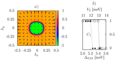
The properties of the BHZ model, along with the relevant parameters , , etc. , are discussed in detail in Refs. Bernevig et al., 2006 and Qi and Zhang, 2011, and summarized in App. B. The -component is defined as , which corresponds to the separation of and Fig. 1c. In Fig. 4a) we plot (color plot) and (arrows) using the exact solutions for the energy bands 2 and 3 in Fig. 1c) and 2.
IV.4 Topological index
From the -vector we calculate numerically the topological invariant Bernevig et al. (2006)
| (28) |
for fixed superlattice parameters meV and meV and varying and fixed meV and varying the (gate-controllable) superlattice parameter , keeping meV for simplicity. The invariant shows a clear jump when changes sign, either by varying or via , as can be seen in Fig. 4b).
V Strip configuration: edge states.
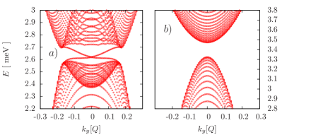
Here we verify the bulk-edge correspondence by explicitly finding the edge states of the system in a finite geometry. We also determine the bulk and edge spectrum for both the topological and non-topological phases, see Fig. 5. We solve the Hamiltonian in Eq. (10) for a strip of width , using hard wall boundary conditions . Bloch’s theorem still applies in the longitudinal -direction. We expand the transverse part of the wavefunction in a normalized sine basis. The number of transverse states is truncated at where is the number of superlattice periods that fit within a strip width. This corresponds to including, roughly, -vectors in the -direction in the bulk model. Solving Eq. (10) for a given value of yields eigenvalues. Focusing on the eigenvalues in the energy interval corresponding to the BHZ bands, one can plot the relevant set of eigenvalues as function of .
V.1 Gapless edge dispersion
In Fig. 5a) the value of meV corresponds to the topological phase (see inset in Fig. 2) and indeed we see edge states in the gap. In Fig. 5b) the even-odd splitting is increased to meV and the edge states are absent, since the system has now turned to a normal insulator. As can be seen in Fig. 2 controls the magnitude and the sign of the gap. Using the BHZ notation, the edge state in Fig. 5a) corresponds to a negative gap , Fig. 5b) where is positive and no gap states appear. Note that for meV our system can not be approximated by an effective BHZ model as the bands show substantial non-parabolicity. This does not influence the existence of the edge states in our system.
V.2 Oscillatory decaying edges.
In order to compare our results to the known analytical solution of the BHZ model, we focus on meV. We can extract the BHZ parameters directly by fitting the curves appearing in the inset of Fig. 2 to the eigenstates of the BHZ model, i.e. Eq. (5) in Ref. Qi and Zhang (2011). From these values we can calculate the properties of the edge states using the ansatz Qi and Zhang (2011); Zhou et al. (2008); michetti12:124007 . Solving for in the middle of the gap ( and ) results in
| (29) |
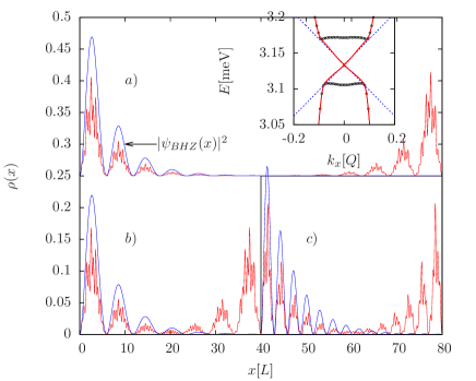
Note that for the parameters extracted from the bulk spectrum , which yields a with a non-zero imaginary part in addition to a real part. This gives rise to a localized edge state that oscillate spatially. Indeed we see from the numerical diagonalization of Eq. (10) that the edge state decays into the bulk with slower oscillations due to the imaginary part of and rapid oscillations due to the period of the superlattice. The probability densities of the edge states corresponding to meV for strip widths and are shown in Figs. 6a) and b), respectively. For meV the decay length and oscillation wavelength are where and , respectively. For a given energy in the gap there are two edge states localized at opposite edges, localized around and localized around . The density of the BHZ edge state localized around , using parameters extracted from Fig. 2 and ,
| (30) |
agrees well with the numerical results (blue curves in Fig. 6). Note that the edge state density is symmetric for Zhou et al. (2008). The helical character of the edge-states comes from the time reversed part of the hamiltonian, see discussion below Eq. (8). Figure 6b) shows the edge state probability density for meV corresponding to meV, which is around a one fourth of that in Fig. 6c) which corresponds to meV. The density in Fig. 6c) shows an oscillation period close to twice as large, reflecting that oscillations are dominated by the quantity , see Eq. (29). Note that experiments based on detecting the edge transport Brune et al. (2012) and scanning gate microscopy that can image the modulation of the edge charge density profile koenig are feasible.
A potential drawback of our proposal is the relative small size of the gap meV, see Supplementary Material. However, what mitigates this is the improved transport properties of high quality InxGa1-xAs materials, as compared to HgTe based systems. Optimizing the quantum wells can yield a 3-fold increase in Grundler , tuning the superlattice parameters will give a factor 2, and pushing down the period to nm, yields a gap meV. This lowers the requirements on the sample mobility and temperature of the experiments. On the positive side, our proposal is unique in that it involves only electrons in standard III-V quantum wells where the parameters leading to band inversion – the superlattice potential ( and ), Fermi energy, charge density and – are easily controllable.
This work was supported by the Icelandic Research Fund, the Brazilian funding agencies CNPq and FAPESP and PRP/USP within the Research Support Center Initiative (NAP Q-NANO). SIE would like to acknowledge helpful discussions with H.G. Svavarsson and G. Thorgilsson for assistance with graphics.
Appendix A The role of and
The mass gap is controlled by two parameters: the energy splitting of the two lowest even and odd double quantum well states and the ’bandwidth’ of the energy bands introduced in the previous section.
For large enough barriers, which is the case in our double barrier, the width of the central barrier is the major factor in controlling . By varying the barrier thickness the value of can be controlled, but it will be fixed for a given sample. The even-odd splitting is predominantly determined by the quantum well structure, i.e. barrier thickness, quantum well width etc. and it is almost unaffected by the presence of the periodic potential. In the absence of the lateral superlattice, and after projecting the full double quantum well Hamiltonian onto the, even/odd subspace results in
| (31) |
where is the Pauli matrix for the double quantum well even-odd subspace. We now assume that the electrostatic potential can be written as a periodic function in and , see Eq. (3) in manuscript. The constants and are replaced by functions and
| (32) | |||||
and when inserted into the Laplace equation jackson , results in the following equations
| , | (33) | ||||
| , | (34) |
The solution to these equations are
| (35) | |||||
| (36) |
where is the distance from the surface to the quantum well. Here we have also assumed that , where is the QW width. When the Hamiltonian with the full electrostatic potential is projected onto the even-odd substace we get
where is given in Eq. (9) and
| (38) |
is a dimensionless constant of order one coming from the matrix element of Eqs. (35) and (36) in the the even and odd basis. We can disregard the mixing of the even and odd states due to lateral periodic potential (the term) as long as
| (39) |
Note that can be controlled by the quantum well structure, e.g. it can be made larger by a thinner barrier, so this condition can always be satisfied. For typical quantum wells the barrier and well thicknesses, are of order nm and the lower limit of periodic potential is nm. So, even for relatively thick barriers and short period superlattice we have . The estimate in Eq. (39) is obtained by comparing the two terms that multiply and in Eq. (LABEL:eq:DQWper). Since the contribution of the different Pauli matrices are added as squares, the condition for discarding the comes from comparing the squares of the two contributions, which leads to Eq. (39).
Appendix B Connection to BHZ model
In the BHZ modelBernevig et al. (2006); Qi and Zhang (2011) the two bands that comprise the inverted bands are written as
| (40) | |||||
| (41) |
where . The bands will only cross when and or when and . The parameter is simply a trivial energy shift whose value has not impact on the physical properties of the system. These two bands are then coupled, with a coupling strength , resulting in a matrix
| (44) | |||||
| (45) |
where and the vector is given by
| (46) | |||||
| (47) | |||||
| (48) |
Here we put the trivial constant . The energy difference between the two bands, in the absence of the spin-orbit coupling, is given by . Note that the full full BHZ model is obtained by constructing a block diagonal matrix with the upper diagonal is the above matrix and the lower one the time reversed version of Eq. (45). The BHZ parameter was introduced in Eq. (8) in the manuscript and the other parameters can be related to band parameters in our proposal as follows:
| (49) | |||||
| (50) | |||||
| (51) |
References
- Kane and Mele (2005) C.L. Kane and E.J. Mele, Phys. Rev. Lett. 95, 226801 (2005).
- Bernevig et al. (2006) A. Bernevig, T.L. Hughes, and S.-C. Zhang, Science 314, 1757 (2006).
- König et al. (2007) M. Konig, S. Wiedmann, C. Brüne, A. Roth, H. Buhmann, L. Molenkamp, X.-L. Qi, and S.-C. Zhang, Science 318, 766 (2007). See also G. M. Gusev et al. Phys. Rev. Lett. 110, 076805 (2013).
- (4) M. Z. Hasan, C. L. Kane, Rev. Mod. Phys. 82, 3045–3067 (2010)
- Qi and Zhang (2011) X. Qi and S.-C. Zhang, Rev. Mod. Phys. 83, 1057 (2011).
- Pankratov et al. (1987) O. Pankratov, S. Pakhomov, and B. Volkov, Solid State Commun. 61, 93 (1987).
- (7) M. Konig et al. Phys. Rev. X 3, 021003 (2013).
- Liu et al. (2008) C. Liu, T.L. Hughes, X.-L. Qi, K. Wang, and S.-C. Zhang, Phys. Rev. Lett. 100, 236601 (2008).
- (9) P. Michetti, J.C. Budich, E.G. Novik, and P. Recher, Phys. Rev. B 85, 125309 (2012)
- Sushkov and Neto (2013) O.P Sushkov and A.H. Castro Neto, Phys. Rev. Lett. 110, 186601 (2013).
- (11) D. Zhang, W. Lou, M. Miao, S. C. Zhang, and K. Chang, Phys. Rev. Lett. 111, 156402 (2013).
- (12) Some experimental evidence for the proposal in Ref. Liu et al. (2008) is reported in I. Knez, R.R. Du, and G. Sullivan, Phys. Rev. Lett. 107, 136603 (2011).
- Calsaverini et al. (2008) R.S. Calsaverini, E.S. Bernardes, J.C. Egues, and D. Loss, Phys. Rev. B 78, 155313 (2008).
- (14) E. Bernardes et al. Phys. Rev. Lett. 99, 076603 (2007); S.I. Erlingsson, J.C. Egues and D. Loss, Physica E 40 1484 (2008).
- (15) F.G.G. Hernandez et al. Phys. Rev. 88, 161305(R) (2013).
- (16) C. Kittel, Introduction to Solid State Physics (Wiley Publishing, 1995), see chapter 7.
- (17) T. Schlosser, K. Ensslin, J.P. Kotthaus, and M. Holland. Europhys. Lett. 33, 683 (1996)
- (18) Different magnitudes of and in Eq. (9) are achieved by making the central holes deeper or shallower than those at the unit cell corners. This pattern is then inherited by the metal deposited on top thus leading to a modulated electric potential within the QW upon the application of a proper gate potential.
- Li et al. (2008) J. Li, K. Chang, G. Hai, and K. Chen, Appl. Phys. Lett. 92, 152107 (2008).
- Zhou et al. (2008) B. Zhou, H.-Z. Lu, R.-L. Chu, S.-Q. Shen, and Q. Niu, Phys. Rev. Lett. 101, 246807 (2008).
- (21) P. Michetti, P.H. Penteado, J.C. Egues, and P. Recher, Semicond. Sci. Technol. 27 124007 (2012)
- (22) The BHZ parameter values corresponding to are meV, meVnm2, meV, meVnm2 and meVnm.
- (23) D. Grundler, Phys. Rev. Lett. 84, 6074 (2000).
- Brune et al. (2012) C. Brune, A. Roth, H. Buhmann, E. Hankiewicz, L. Molenkamp, J. Maceijko, X.-L. Qi, and S.-C. Zhang, Nature Physics 8, 485 (2012).
- (25) N.W. Ashcroft and N.D. Mermin, Solid state physics, Saunders, 1976 [see figure 9.4]
- (26) J.D. Jackson, Classical electrodynamics,3rd ed. , Wiley and Sons, 1999