Spectroscopy of snake states using a graphene Hall bar
Abstract
An approach to observe snake states in a graphene Hall bar containing a pn-junction is proposed. The magnetic field dependence of the bend resistance in a ballistic graphene Hall bar structure containing a tilted pn-junction oscillates as a function of applied magnetic field. We show that each oscillation is due to a specific snake state that moves along the pn-interface. Furthermore depending on the value of the magnetic field and applied potential we can control the lead in which the electrons will end up and hence control the response of the system.
pacs:
72.80.Vp, 73.23.Ad, 85.30.FgGraphene’s electronic properties are drastically different from conventional semiconductors. Graphene has a linear spectrum near the and points with zero gapf1 ; f2 which causes perfect transmission through arbitrarily high and wide barriers for normal incidence, referred to as Klein tunneling f3 ; f4 ; f5 ; f6; f7 . The metamaterial character of pn-junctions in graphenechei07 was pointed out earlier, and focusing of electronic waves was proposedMatu1 ; has10 . The metamaterial properties of the above mentioned pn-junctions resulted in the expectancy of controlling the electron wave function, in particular, the width of electron beams by means of a superlattice that is known as collimation Cheol . Qualitatively, the metamaterial properties of pn-junctions in graphene can be understood by inspecting classical trajectoriesA2 , or using ray optics as it is called in the case of electromagnetic phenomenaA1. Classical simulations for electronic transport were done recently for a Hall bar made of single layerA3 ; cMLG and bilayerAM2 graphene. Gapless energy dispersion of graphene allows electron and hole switching at the pn-interface which can be realized using nanostructured gates mrm1 ; mrm2 .
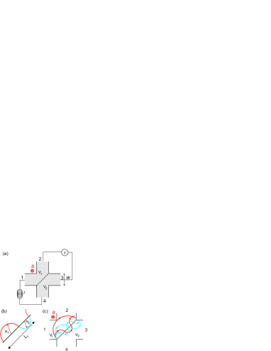
Applying a nanostructured top gate or side gates one can induce a pn-interface in the Hall cross as shown schematically in Fig. 1(a). Near the interface conduction by electrons on one side and conduction by holes on the other side occurs. An applied magnetic field bends electron and hole trajectories towards the interface while Klein tunneling through the interface allows snake orbits to propagate (see Fig. 1(b)). Snake states along the pn-interface were predicted analytically Ma1 ; Ma2 in the presence of a homogeneous magnetic field. Existence of such states was confirmed in recent experiments Marcus1 ; Marcus0 by measuring the resistance along the pn-interface.
Here we showed that by using a tilted pn-interface in the cross of a Hall bar structure allows us to characterize the different snake states by measuring the bend resistance. In such a device carriers injected from any lead ( Fig. 1(c) shows injection from lead 1) will transmit multiple times on the pn-interface and move along it until they reach one of the leads at the other end (lead 2 or lead 3 in Fig. 1(c)). The choice of the final lead depends on the value of applied magnetic field, carrier density, length of the pn-interface and the angle of injection. We found that as a function of the magnetic field strength or the Fermi energy a sequence of peaks and dips appear in the bend resistance depending in which lead the carriers will end up. This effect can also be viewed as a type of magnetic focusing, but unlike normal transverse magnetic focusingTMF which is a result of skipping orbits, here the focusing appears due to snake states.
We can control the position of the peaks by changing the cyclotron radius which is given by,
| (1) |
where is the carrier density, is the Fermi energy, is the applied potential, is the Fermi velocity and is the applied magnetic field. Thus we are able to control the snake states in graphene by changing the magnetic field or carrier density.
To simulate the transport properties of such a graphene Hall bar we rely on the semiclassical billiard modelcBM . In this model electrons are considered as point particles (billiards) which are injected uniformly over the length of the lead, while the angular distribution is given by , with . The model is justified when , where is the Fermi wavelength and the width of the lead and when quantization effects are not important. This approach has been used to describe various experiments with a mesoscopic Hall barA3 ; cBM ; cSCA ; cSCA4 ; cSCA5 . The motion of ballistic particles is determined by the classical Newton equation of motion, which is justified for the case where is the phase coherence length and the mean free path (for typical parameters at low temperatures the electron mean free path can be calculated as , with the mobility and the electron density), while the transmission of electrons and holes through the pn-interface is calculated quantum mechanically using the Dirac Hamiltonian.
Transport properties of the system are obtained by using the Landauer-Büttiker formalism. For this purpose we need to find the electron transmission probabilities between the different leads of the Hall bar structure. The probability that an electron injected from terminal will end up in terminal is given by . These transmission probabilities are then used in the Landauer-Büttiker formula in order to calculate the current in terminal ,
| (2) |
here is the number of occupied transport channels, which depends on and and are the chemical potentials of the reservoirs and , respectively, is the electron charge and is Planck’s constant. Eliminating the chemical potentials we can derive expressions for the different resistances,
| (3) |
with and
| (4) |
where . In the present paper, we
are interested in the bend resistance .
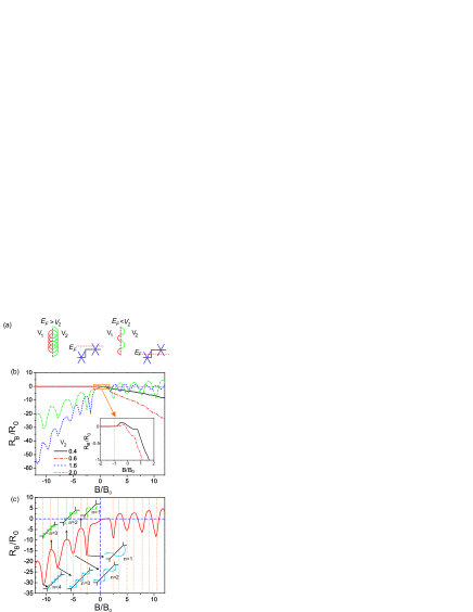
The four-terminal Hall bar with a tilted pn-interface is used as the device of interest. For numerical calculations we used meV, and meV. For a typical electron density , and a width of leads , and , we obtain for the unit of magnetic field , and and for the resistance unit , and . The cyclotron radius is given by Eq. (1) which for results into . The numerical simulation of the bend resistance as a function of the magnetic field is shown in Figs. 2(b) and 2(c). Two different regimes are found:
1) : the electron can pass through the pn-interface and preserves the direction of motion with a change of the cyclotron radius. One of the possible trajectories is shown in the left panel of Fig. 2(a). Notice that from Eq. (3) the bend resistance is proportional to
| (5) |
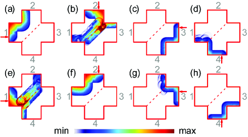
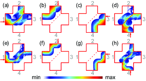
As shown in Fig. 2(b) for negative magnetic field the bend resistance is almost zero. We can understand this behavior better using the electron current density plots, shown in Figs. 3(a)-(d) for . The electron current density for electrons injected from lead 1 (see Fig. 3(a)) shows that the majority of electrons perform skipping orbits on the edge of the system and therefore end up in lead 2 resulting in zero transmission probability in part of Eq. (5). Similarly, shown in Fig. 3(d), none of the electrons travel from lead 4 to lead 3, resulting in zero in part of Eq. (5). Consequently, for high negative magnetic fields the bend resistance is zero. As we approach zero magnetic field the cyclotron radius increases and the electrons will have a chance to travel from lead 1 to 3 or from lead 4 to lead 3. We can find this classically by setting the cyclotron radius to with corresponding magnetic field given by (see the inset of Fig. 2(c) for the position of the classically predicted value of the magnetic field of given by the vertical orange dotted line for ). For positive magnetic field electrons coming from lead travel through the pn-junction with different radius on the two sides of the junction as shown schematically in the left panel of Fig. 2(a) which has a chance to end up in any lead and consequently we have nonzero transmission factors (especially and which appear in Eq. (5)). On the other hand, all electrons injected from lead perform skipping orbits and consequently will end up in lead resulting in a nonzero . However the transmission appearing in Eq. (5) is zero because there is no electrons going from lead into , then the first part of Eq. (5) is zero and only the second part will be nonzero and which is responsible for the negative bend resistance.
2) For we have on one side of the pn-junction electrons and on the other side holes. When an electron transmits through the pn-interface it transforms to a hole and its direction of motion will change which results in a snake state, as shown in Figs. 1(b)-(c) and in Fig. 2(a). Depending on initial factors (angle of injection, magnetic filed, potential, etc…) it can end up in the electron or hole region. This results in an oscillatory behavior of the bend resistance as shown in Figs. 2(b) and 2(c). Each of the peaks can be associated with a specific snake state as illustrated schematically in the inset of Fig. 2(c). Peaks occur respectively when the length of the tilted pn-interface () satisfies the equality, which means that the particle injected from lead will most likely end up in lead . Here is the number of times the particle switches between the electron and the hole region along the pn-interface. The corresponding magnetic field is given by,
| (6) |
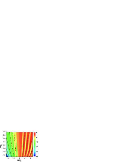
where we use and . A contour plot of the bend resistance as a function of applied magnetic field and electrical potential is plotted in Fig. 4. Figure shows reasonable good agreement between classically predicted peaks (Eq. (6)), shown by the black dashed lines, and our simulations. For the special case when (or ) we find
that the position of the peaks is given by, . The analytical results of Eq. (6) are shown in Fig. 2(c) by the vertical dotted orange lines. We also show schematically the corresponding snake trajectory for each peak and dip for different number of nodes. The distance between consecutive peaks is given by
| (7) |
which for the used parameters results into . In Figs. 5(a)-(d) we plot the electron current densities for which corresponds to a dip in the bend resistance. Figures show that the majority of carriers injected from lead 1 will end up in lead 2. In case of injection from lead 4, carriers are most likely to end up in lead 3. Other transmission coefficients and are small which result in a minimum in the bend resistance. For the magnetic field , which corresponds with a peak, most electrons injected from lead will end up into lead and electrons injected from lead will end up into lead which means that part I in Eq. (5) will be much larger than part II.
In summary, using a tilted pn-interface we are able to selectively probe different snake states and investigate its influence on the transport properties of a graphene Hall bar. Such a pn-junction along the diagonal of the Hall bar cross can be realized experimentally. As our numerical simulation showed, applying different magnetic field (or different potential) we are able to control the electron current along the pn-interface. This resulted in an oscillatory behavior of the bend resistance which is a signature of the different snake states appearing in the system. We found an analytical formula that predicts the position of the peaks and dips in the resistance.
This work was supported by the Flemish Science Foundation (FWO-Vl), the European Science Foundation (ESF) under the EUROCORES Program EuroGRAPHENE within the project CONGRAN and the Methusalem Foundation of the Flemish government.
References
- (1) K. S. Novoselov, A. K. Geim, S. V. Morozov, D. Jiang, M.I. Katsnelson, I. V. Grigorieva, S. V. Dubonos, and A. A. Firsov, Nature (London) 438, 197 (2005).
- (2) Y. Zheng, Y. W. Tan, H. L. Stormer, and P. Kim, Nature (London) 438, 201 (2005).
- (3) M. I. Katsnelson, K. S. Novoselov, and A. K. Geim, Nature Physics 2, 620 (2006).
- (4) Vadim V. Cheianov, Vladimir Faĺko, and B. L. Altshuler, Science 315, 1252 (2007);
- (5) O. Klein, Z. Phys. 53, 157 (1929).
- (6) J. M. Pereira Jr., V. Mlinar, F. M. Peeters, and P. Vasilopoulos, Phys. Rev. B 74, 045424 (2006).
- (7) V. V. Cheianov, V. Fal’ko, and B. L. Al’tshuler, Science 315, 1252 (2006).
- (8) A. Matulis, M. Ramezani Masir, and F. M. Peeters, Phys. Rev. B 83, 115458(2011).
- (9) F. Hassler, A. R. Akhmerov, and C. W. J. Beenakker, Phys. Rev. B 82, 125423 (2010).
- (10) C. H. Park, F. Giustino, M. L. Cohen, and S. G. Louie, Nano Lett. 9, 1731 (2009).
- (11) A. Matulis, M. Ramezani Masir, and F. M. Peeters, Phys. Rev. A 86, 022101 (2012).
- (12) M. Barbier, G. Papp, and F. M. Peeters, Appl. Phys. Lett. 100, 163121 (2012).
- (13) S. P. Milovanović, M. Ramezani Masir, and F. M. Peeters, J. Appl. Phys. 113, 193701 (2013).
- (14) S. P. Milovanović, M. Ramezani Masir, and F. M. Peeters, J. Appl. Phys. 114, 113706(2013).
- (15) J. R. Williams, L. DiCarlo, C. M. Marcus, Science, 317 5838 (2007).
- (16) H. -Y. Chiu, V. Perebeinos, Y. Lin, and P. Avouris, Nano Lett. 10, 4634 (2010).
- (17) P. Carmier, C. Lewenkopf, and D. Ullmo, Phys. Rev B 84, 195428 (2011).
- (18) N. Davies, A. A. Patel, A. Cortijo, V. Cheianov, F. Guinea, and V. I. Fal’ko, Phys. Rev. B 85, 155433 (2012).
- (19) J.R. Williams and C.M. Marcus, Phys. Rev. Lett. 107, 046602 (2011).
- (20) J. R. Williams, T. Low, M. S. Lundstrom, and C. M. Marcus, Nature Nanotechnology 6, 222 (2011).
- (21) T. Taychatanapat, K. Watanabe, T. Taniguchi and P. Jarillo-Herrero, Nature Physics 9, 225(2013).
- (22) C. W. J. Beenakker and H. van Houten, Phys. Rev. Lett. 63, 17 (1989).
- (23) P. Carmier, C. Lewenkopf, and D. Ullmo, Phys. Rev. B 81, 241406 (2010).
- (24) M. L. Roukes, A. Scherer, and B. P. Van der Gaag, Phys. Rev. Lett. 64, 10 (1990).
- (25) F. M. Peeters and X. Q. Li, App. Phys. Lett. 72, 572 (1998).
- (26) K. S. Novoselov, A. K. Geim, S. V. Dubonos, Y. G. Cornelissens, F. M. Peeters, and J. C. Maan, Phys. Rev. B 65, 233312 (2002).
- (27) B. J. Baelus and F. M. Peeters, Appl. Phys. Lett. 74, 1600 (1999).