Optical manipulation of the exciton charge state in single layer tungsten disulfide
Abstract
Raman scattering and photoluminescence (PL) emission are used to investigate a single layer of tungsten disulfide (WS2) obtained by exfoliating n-type bulk crystals. Direct gap emission with both neutral and charged exciton recombination is observed in the low temperature PL spectra. The ratio between the trion and exciton emission can be tuned simply by varying the excitation power. Moreover, the intensity of the trion emission can be independently tuned using additional sub band gap laser excitation.
I Introduction
Layered compounds involving transition metals from group VI and chalcogens (the so-called dichalcogenides) are promising candidates for exploring atomically thin structures. The basic building block consists of a monolayer of a transition metal with a chalcogen monolayer above and below. We refer to this chalcogen-metal-chalcogen stack as a single layer. All the dichalcogenides have a strong intra layer chalcogen-metal covalent bond while, the layers are weakly held together by van der Waals forces. Nevertheless, the inter layer coupling plays a significant role in determining the band structure. Bulk crystals are semiconductors with an indirect gap in the near infrared spectral range. In contrast, single layer transition metal dichalcogenides such as molybdenum disulfide (MoS2), tungsten disulfide (WS2) or tungsten diselenide (WSe2) are two dimensional (2D) semiconductors with a direct gap in the visible spectral range. Mak et al. (2010); Splendiani et al. (2010); Eda et al. (2011); Albe and Klein (2002); Gutiérrez et al. (2013); Zhao et al. (2013); Wang et al. (2012); Cao et al. (2012); Mak et al. (2013) The optical response of a single layer of these materials is dominated by excitonic effects; the optical spectrum is characterized by the presence of two low-energy exciton peaks (A and B excitons) that arise from vertical transitions from a spin-orbit-split valence band to a doubly degenerate conduction band at the K point of the Brillouin zone. Frey et al. (1998); Klein et al. (2001); Ramasubramaniam (2012)
The physics of excitons in 2D semiconductors is known to be extremely rich once additional carriers are introduced into the system; the optical spectra consist of emission from both neutral (X) and charged excitons (X±). Charged excitons were discovered in II-VI and III-V quantum wells (QWs). Kheng et al. (1993); Finkelstein et al. (1995) In GaAs QWs it has been shown that the ratio between neutral and charged exciton can be tuned by using a back gate, Groshaus et al. (2007); Bar-Joseph (2005); Finkelstein et al. (1995) or additional illumination. Shields et al. (1995); Glasberg et al. (1999); Jadczak et al. (2012) In CdTe QWs this ratio can simply be tuned using additional illumination or a change of the excitation power. Huard et al. (2000); Esser et al. (2000); Kossacki et al. (1999) Recently, it has been shown that a gate can be used to tune the carrier density in single layer molybdenum disulfide and molybdenum diselenide. Mak et al. (2013); Ross et al. (2013) While in standard semiconductors the dissociation energy of the charged exciton is relatively small ( few meV), in exfoliated dichalcogenides this energy is approximately an order of magnitude larger. Hence, the ability to control the exciton charge state in semiconductor structures which emit light at room temperature and in the visible range, is expected to open many possibilities for optoelectronics applications.
In this paper we show that in a single layer of tungsten disulfide (WS2) obtained by the exfoliation of n-type bulk crystals, we observe both charged and neutral exciton recombination in the photoluminescence (PL) emission spectra. Additionally, by simply changing the intensity of the laser excitation, we can tune the ratio between the trion and exciton emission which demonstrates our ability to tune the density of 2D carriers with light. Moreover, using additional sub band gap laser excitation, the trion emission intensity can be independently tuned. Finally, the temperature dependence of the direct gap of a WS2 single layer is shown to follow the usual behavior for a semiconductor.
II Experiment
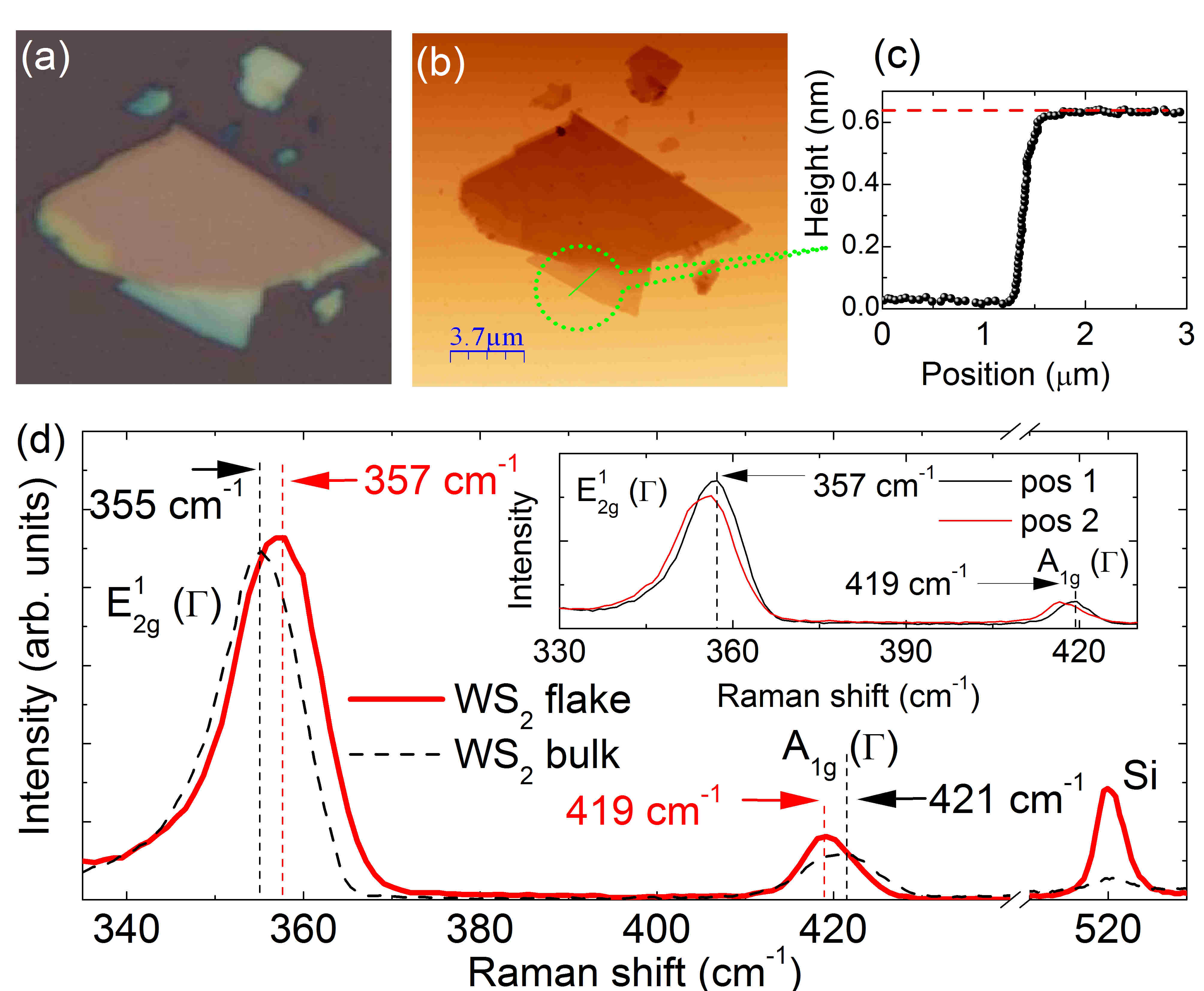
Single and few layer flakes of tungsten disulfide (WS2) have been obtained by mechanical exfoliation of bulk 2H-WS2 (the hexagonal 2H-polytype of tungsten disulphide) single crystals grown using chemical vapor transport with Bromine as the transport agent. Samples obtained in this way are naturally n-type. El-Mahalawy and Evans (1977) Hall measurements on bulk crystals reveal an electron density cm-3 at room temperature, which decreases rapidly at lower temperatures and is only cm-3 at K. After exfoliation, the WS2 flakes were placed on silicon substrate. Flakes with single layer regions have been identified using optical microscopy, atomic force microscopy (AFM) and Raman spectroscopy. Typical results are presented in Fig 1. Parts of the flake (subsequently referred to as flake 1), which are single layer have a characteristic blue color in the optical microscope image and are also visible in the AFM image. The AFM height profile, measured moving along the green line indicated on the AFM image, is shown Fig 1(c). The 0.6 nm step in the AFM height profile corresponds to a single layer WS2.Schutte et al. (1987)
For the measurements the sample was placed in an optical cryostat mounted on motorized translation stages. Excitation and collection was implemented using an external microscope objective giving a typical spot diameter of m. The PL and -Raman spectra have been recorded using a spectrometer equipped with a CCD camera and a laser emitting at nm was used for excitation. For some measurements the sample was simultaneously illuminated by a Ti:Sapphire laser centered at 860 nm, with the laser beams entering collinearly to the microscope objective.
III Micro-Raman and micro-PL
Representative Raman spectra, obtained for a single layer region of flake 1(red line) and a bulk crystal (black dashed line), are shown in Fig 1(d). The bulk crystal shows two Raman peaks at cm-1 and cm-1 corresponding to the well known active Raman modes and . However, for the single layer these two peaks shift towards each other by cm-1. These results are consistent with previously reported theoretical calculations and measurements on single layer of tungsten disulfide. Albe and Klein (2002); Gutiérrez et al. (2013); Zhao et al. (2013) Hence, independently of the AFM measurements, the Raman data provides an additional confirmation of the single layer character of the investigated regions of our flakes.
Fig. 2 shows typical PL spectra measured on a single layer region of two different flakes as a function of the excitation power at K. Panel (a) corresponds to results obtained on flake 1. In both cases, at low excitation powers, we observe strong emission around 2 eV which corresponds well with the predicted recombination of the neutral exciton A across the direct gap of single layer WS2. Klein et al. (2001) Moving around the flake the measured emission energy can vary slightly around this value Gutiérrez et al. (2013) which we attribute to strain as the Raman spectra show simultaneous small rigid shift of the two Raman peaks with no change in the peak separation (see inset of Fig 1 d). This is consistent with the reported influence of the strain on the optical properties of a single layer of MoS2. Conley et al. (2013); Rice et al. (2013)
III.1 Neutral and charged exciton emission
Perhaps the most striking feature of the PL spectra is that we observe a second emission line on the low energy side of the neutral exciton emission at around meV. This line, which becomes much stronger as the excitation power is increased, is observed in all the flakes we have measured (see e.g. data for flake 2 in Fig 2(b). We will see below that the behavior of the low energy line has all characteristics of a trion; with increasing excitation power, the intensity increases linearly (bi-exciton has quadratic dependence), the binding energy varies linearly, while the ratio of the trion and neutral exciton emission intensity is not constant.
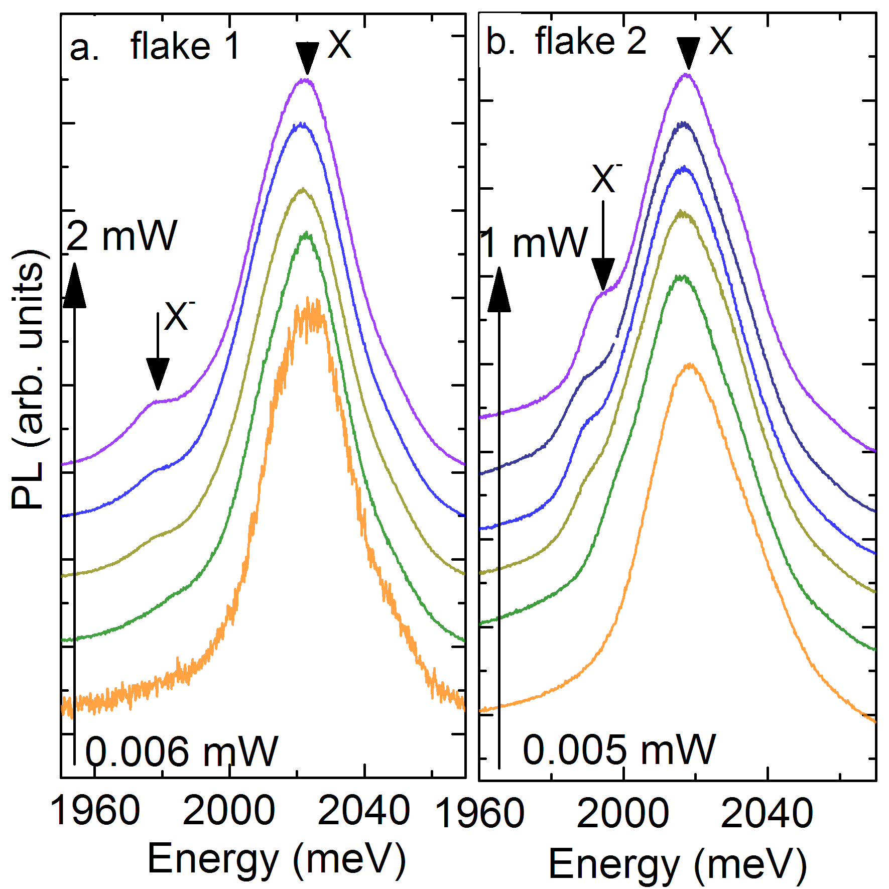
The neutral exciton is the ground state of a charge neutral system and trions are only formed in the presence of excess charge which therefore directly controls the intensity of the trion emission. Thus, trion emission is usually not observed in exfoliated samples of MoS2 and WS2 unless a gate is used. Eda et al. (2011); Mak et al. (2010); Splendiani et al. (2010); Gutiérrez et al. (2013) Gated samples can exhibit an additional line meV below the excitonic line which is attributed to the emission from charged excitons (X±). Mak et al. (2013); Ross et al. (2013) Simply by varying the applied gate voltage it is possible to tune the ratio between neutral and charged exciton emission. Hence, in our ungated samples, we attribute the low energy line to emission from charged excitons (trions) which we presume to be negatively charged given the n-type nature of the bulk crystals. The observation of a requires the presence of excess electrons in the conduction band. In our truly 2D samples internal electric fields cannot spatially separate oppositely charged particles which makes it almost impossible to create excess charge from photo-created electron-hole pairs. However, at low temperature Hall data on the bulk crystals shows that the carriers are frozen out onto the donor levels. Nevertheless, laser illumination, in addition to creating electron-hole pairs, is expected to dynamically photo-ionize carriers trapped on the donors at low temperature, creating a non equilibrium excess electron density in the conduction band. Therefore, we expect that the intensity ratio between neutral and charged exciton can simply be tuned by the varying the power of the laser. To see this more in detail we have analyzed the energy and the intensity of the emission of both X and X- as a function of the excitation power. The data has been fitted using two gaussian functions to extract the intensity and position of the two lines. The analysis, performed on flakes 1 and 2, is presented in Fig 3(a),(c).
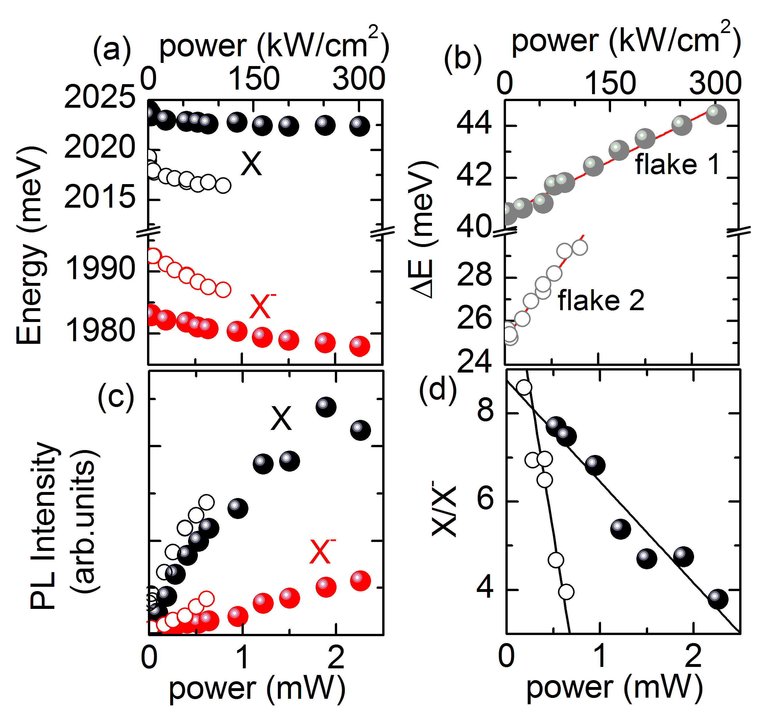
Fig 3(a) shows the power dependence of emission energy of the charged and the neutral exciton. With increasing excitation power the neutral and charged exciton emission red shifts towards lower energies with a larger change for the trion. The difference , between the emission energy of X and X-, is the dissociation energy of the trion which is presented in Fig 3(b). The trion dissociation energy grows linearly with the excitation power suggesting that the density of the carriers also grows linearly with the laser power: The difference in the energy can be expresses as sum of the binding energy and Fermi energy (). Huard et al. (2000) Here binding energy is defined as the dissociation energy in the limit of infinitively small doping () where is the energy needed to promote one electron from the trion to the bottom of the conduction band. The Fermi energy increases with increasing power of illumination (photon flux) due to the photo-ionization of donors. The trion dissociation energy (Fermi energy) increases more rapidly with laser power in flake 2 suggesting a larger concentration of donors in this flake. As the carrier concentration increases, the trion dissociation energy increases and we can tune it over approximately 4 meV for both flakes. Such a behavior is also observed in II-VI QWs where the interplay between exciton and charged exciton was achieved using external illumination of the sample. Kossacki et al. (1999, 2004) The enhanced trion binding energy, compared to standard semiconductors, is linked to the true 2D character of the dichalcogenides and the larger effective mass. Ramasubramaniam (2012)
The calculated integrated intensity of the emission of the charged and neutral exciton, is presented in Fig. 3(c). For both lines the emission intensity increases with increasing power, however, the increase is not the same for the neutral and the charged exciton. To illustrate this the exciton/trion intensity ratio is plotted as a function of laser power in Fig. 3(d). For both flakes the ratio of the integrated intensities decreases with the excitation power by a factor of more than . This is due to increase probability of the creation of the trion with increasing the density of the photo-ionized carriers. However, as the above gap green laser illumination also creates electron hole pairs, the intensity of the neutral exciton emission also increases with laser power. The decrease of the intensity ratio is much faster for the second flake as can also seen directly in the spectra in Fig 2 (b), where the trion line is rapidly becoming stronger with increasing excitation power. Again, the increased sensitivity to laser power is consistent with a larger density of donor impurities in flake 2. Note, that for both flakes we remain in the linear regime for the trion emission (the exciton emission shows some signs of saturation), so that even at maximum laser power a significant proportion of the donors are still neutral.
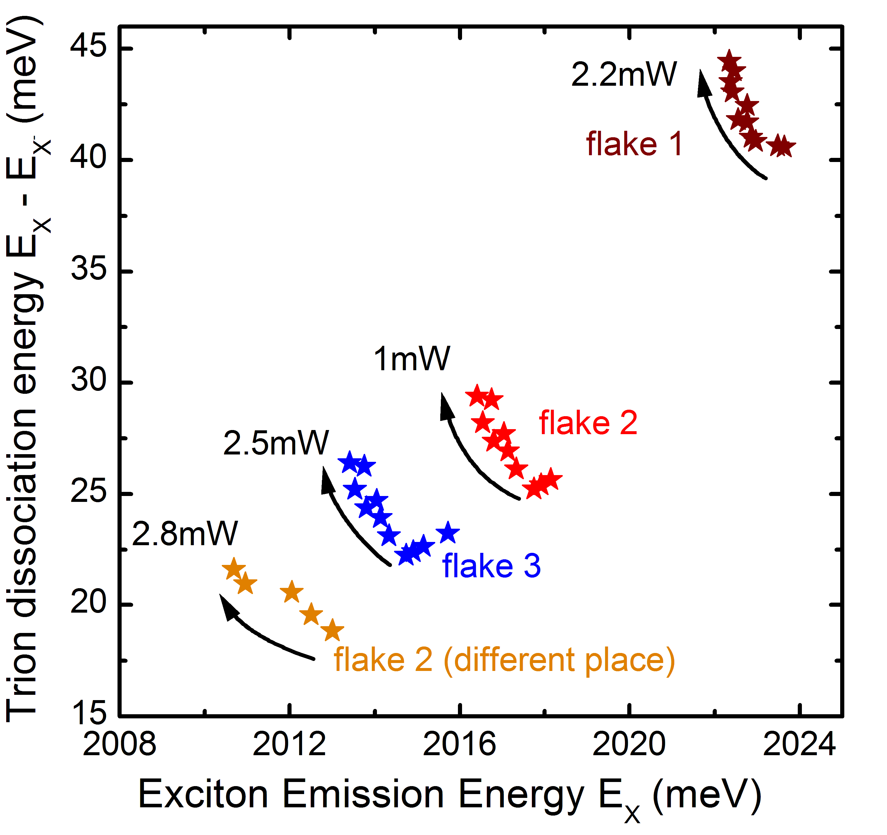
In Fig. 4 we plot the trion dissociation energy () as a function of the exciton emission energy () for three different flakes. For a given flake the trion dissociation energy could be tuned over small range by varying the power of the 532nm excitation. As previously discussed, with increasing power the trion dissociation energy increases due to the increase in the carrier density (Fermi energy). For all flakes we can tune the trion dissociation energy over a range of meV. The increase in the trion dissociation energy is accompanied by a small decrease ( meV) of the exciton emission energy which we attribute to an increase in the exciton binding energy due to the reduced screening by trions which are in a spin singlet state and therefore cannot screen effectively due to the Pauli principle. It is important to note that there is a considerable increase meV in the trion dissociation energy when going from flake 3 to flake 1, which is accompanied by a smaller increase meV in the exciton emission energy. Within the 2D hydrogen model the exciton binding energy is , where is the effective Rydberg, and the trion dissociation energy is . Ross et al. (2013) From flake to flake the trion dissociation energy varies in the range meV corresponding to a change in exciton binding energy within the 2D hydrogen model from to meV. The observed increase in the exciton emission energy is much smaller ( meV) so that the increase in exciton binding energy when going from flake 3 to flake 1 has to be compensated by a similar ( meV) increase in the band gap of the crystal.
III.2 Independently tuning the trion emission
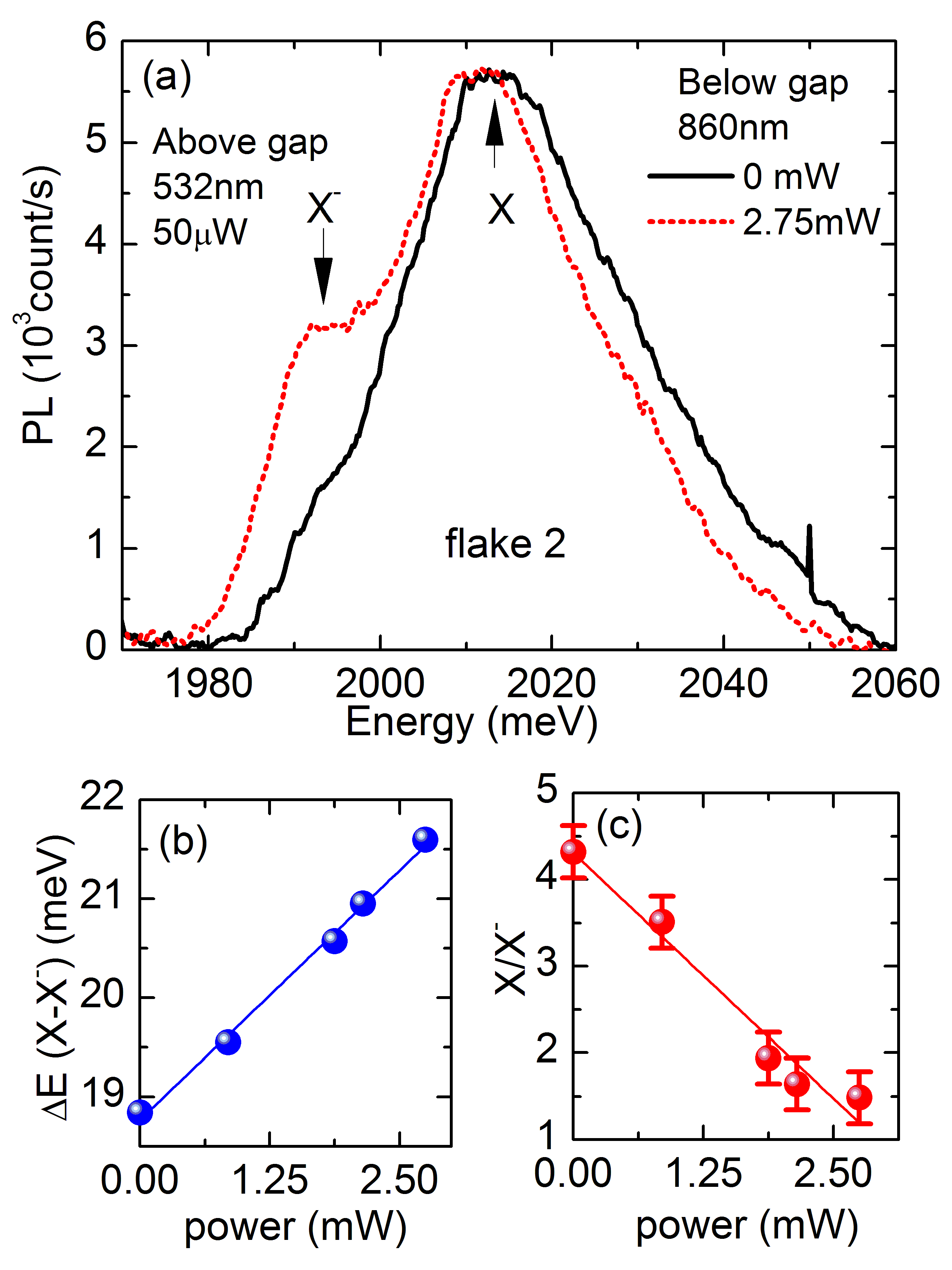
In order to tune the trion and neutral exciton emission independently we have performed PL using two color excitation. A low power (50 W) for the above gap green excitation is used in order to generate a constant density of electron hole pairs together with a small density of photo-ionized electrons. Additional below gap excitation is provided by a laser centered at 860 nm (1441 meV). Photons with this energy, which is well below the gap, do not generate electron-hole pairs. However, their energy is largely sufficient to photo-ionize electrons from the donor level which is a few hundred meV below the indirect conduction band in bulk crystals. Therefore, we expect that the sub band gap radiation can be used to independently tune the excess density of electrons in the sample.
Representative two color spectra measured on flake 2 are presented Fig 5(a). In the absence of below gap illumination, for the low green excitation power chosen, the trion line is very weak. However, when additionally illuminated using a laser at 860 nm, the intensity of the trion emission increases while the (integrated) intensity of the neutral exciton emission decreases. The difference of the emission energy (E) and ratio of the integrated intensity between neutral and charged exciton determined from the full data set are presented in Fig 5 (b) and (c) respectively. We observe that, as for green excitation, the trion dissociation energy E increases linearly with the power of laser and that the intensity ration between neutral and charged exciton also decreases linearly. This demonstrates that below band gap excitation can be used to vary the electron density in the conduction band and thus to independently tune the intensity of the trion emission.
III.3 Temperature dependence of the band gap
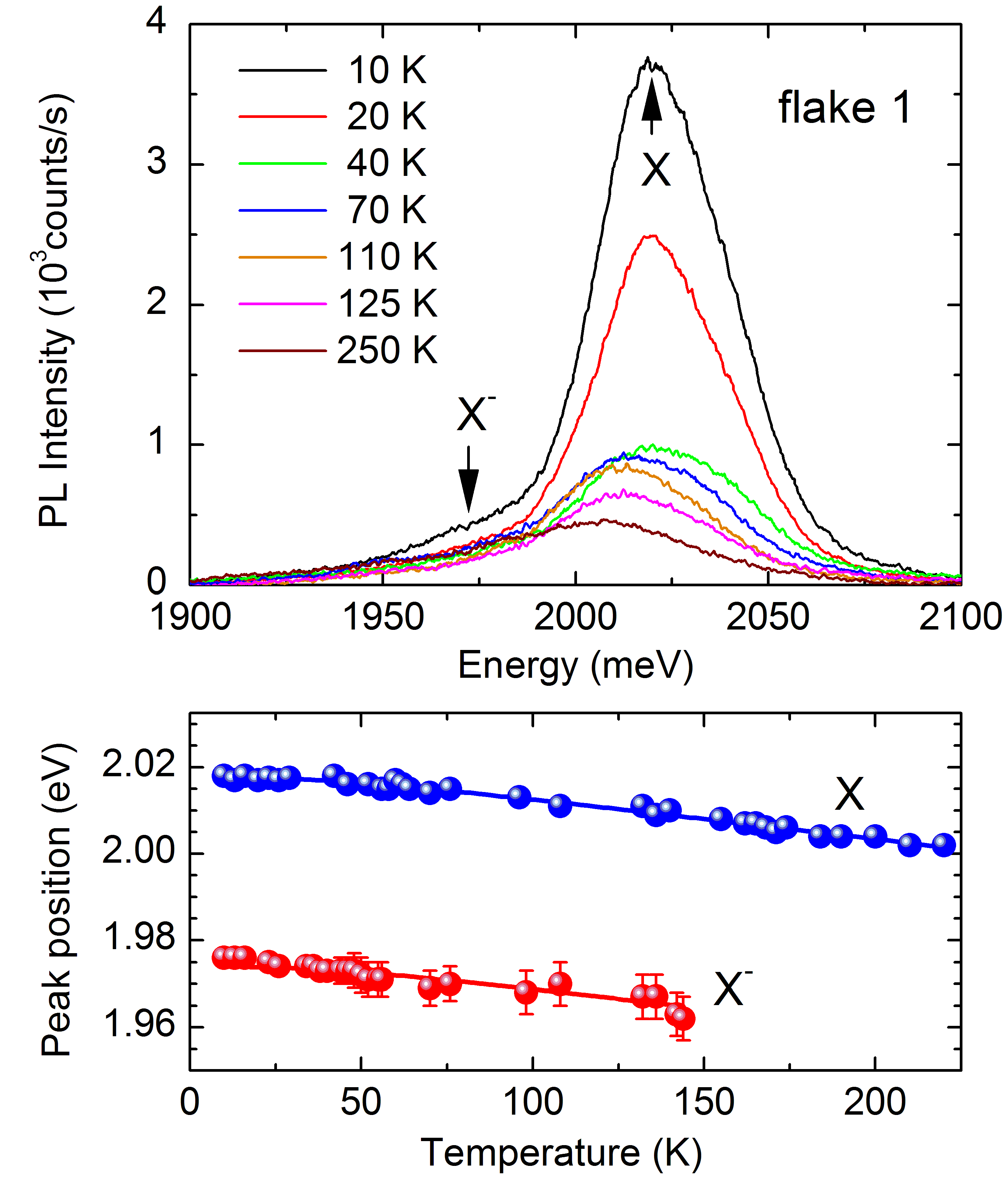
Finally, the temperature dependance of the emission is presented in Fig 6(a). Both exciton lines red shift as the temperatures increases and the charged exciton emission vanishes around 140 K. The energy of the emission, obtained by fitting Gaussians, as a function of the temperature is presented in Fig 6b. Using the standard expression for the temperature dependence of a semiconductor band gap O’Donnell and Chen (1991) we can write an expression for the exciton emission energy as a function of temperature,
| (1) |
where is the emission energy at zero temperature, is a dimensionless coupling constant and is the average phonon energy. The best fit to the neutral exciton is obtained with eV, and meV. The charged exciton is well fitted using the same parameters except for the zero temperature emission energy . Similar values for the average phonon energy and coupling constant have been obtained for tungsten diselenide. Ross et al. (2013).
IV Conclusion
Using PL measurements, we have observed the emission from charged and neutral exciton in an ungated single layer of WS2. The trion emission is closely linked to the n-type nature of our crystals. Using two color PL with above and below band gap illumination we can independently tune the trion/exciton intensity ratio. The below band gap excitations tunes the excess electron density in the conduction band via the dynamic photo-ionization of neutral donors. Since the photo-ionization threshold will be similar to the donor binding energy meV this provides a possible method for the optical detection of far infrared radiation.
Acknowledgements.
AAM acknowledges financial support from the French foreign ministry. This work was partially supported by NEXTVALLEY and by ANR project milliPICS.References
- Mak et al. (2010) K. F. Mak, C. Lee, J. Hone, J. Shan, and T. F. Heinz, Phys. Rev. Lett. 105, 136805 (2010).
- Splendiani et al. (2010) A. Splendiani, L. Sun, Y. Zhang, T. Li, J. Kim, C.-Y. Chim, G. Galli, and F. Wang, Nano Letters 10, 1271 (2010).
- Eda et al. (2011) G. Eda, H. Yamaguchi, D. Voiry, T. Fujita, M. Chen, and M. Chhowalla, Nano Letters 11, 5111 (2011).
- Albe and Klein (2002) K. Albe and A. Klein, Phys. Rev. B 66, 073413 (2002).
- Gutiérrez et al. (2013) H. R. Gutiérrez, N. Perea-López, A. L. Elías, A. Berkdemir, B. Wang, R. Lv, F. López-Urías, V. H. Crespi, H. Terrones, and M. Terrones, Nano Letters 0, 0 (2013).
- Zhao et al. (2013) W. Zhao, Z. Ghorannevis, L. Chu, M. Toh, C. Kloc, P.-H. Tan, and G. Eda, ACS Nano 7, 791 (2013).
- Wang et al. (2012) Q. H. Wang, K. Kalantar-Zadeh, A. Kis, J. N. Coleman, and M. S. Strano, Nature Nanotechnology 7, 699 (2012).
- Cao et al. (2012) T. Cao, G. Wang, W. Han, H. Ye, C. Zhu, J. Shi, Q. Niu, P. Tan, E. W. B. Liu, and J. Feng, Nature Communications 3, 887 (2012).
- Mak et al. (2013) K. F. Mak, K. He, C. Lee, G. H. Lee, J. H. T. F. Heinz, and J. Shan, Nature Materials 12, 207 (2013).
- Frey et al. (1998) G. L. Frey, S. Elani, M. Homyonfer, Y. Feldman, and R. Tenne, Phys. Rev. B 57, 6666 (1998).
- Klein et al. (2001) A. Klein, S. Tiefenbacher, V. Eyert, C. Pettenkofer, and W. Jaegermann, Phys. Rev. B 64, 205416 (2001).
- Ramasubramaniam (2012) A. Ramasubramaniam, Phys. Rev. B 86, 115409 (2012).
- Kheng et al. (1993) K. Kheng, R. T. Cox, M. Y. d’ Aubigné, F. Bassani, K. Saminadayar, and S. Tatarenko, Phys. Rev. Lett. 71, 1752 (1993).
- Finkelstein et al. (1995) G. Finkelstein, H. Shtrikman, and I. Bar-Joseph, Phys. Rev. Lett. 74, 976 (1995).
- Groshaus et al. (2007) J. G. Groshaus, P. Plochocka-Polack, M. Rappaport, V. Umansky, I. Bar-Joseph, B. S. Dennis, L. N. Pfeiffer, K. W. West, Y. Gallais, and A. Pinczuk, Phys. Rev. Lett. 98, 156803 (2007).
- Bar-Joseph (2005) I. Bar-Joseph, Semiconductor Science and Technology 20, R29 (2005).
- Shields et al. (1995) A. Shields, J. Osborne, M. Simmons, M. Pepper, and D. Ritchie, Phys. Rev. B 52, R5523 (1995).
- Glasberg et al. (1999) S. Glasberg, G. Finkelstein, H. Shtrikman, and I. Bar-Joseph, Phys. Rev. B 59, R10425 (1999).
- Jadczak et al. (2012) J. Jadczak, L. Bryja, A. Wójs, and M. Potemski, Phys. Rev. B 85, 195108 (2012).
- Huard et al. (2000) V. Huard, R. T. Cox, K. Saminadayar, A. Arnoult, and S. Tatarenko, Phys. Rev. Lett. 84, 187 (2000).
- Esser et al. (2000) A. Esser, E. Runge, R. Zimmermann, and W. Langbein, Phys. Rev. B 62, 8232 (2000).
- Kossacki et al. (1999) P. Kossacki, J. Cibert, D. Ferrand, Y. Merle d’Aubigné, A. Arnoult, A. Wasiela, S. Tatarenko, and J. A. Gaj, Phys. Rev. B 60, 16018 (1999).
- Ross et al. (2013) J. S. Ross, S. Wu, H. Yu, N. J. Ghimire, A. M. Jones, G. Aivazian, J. Yan, D. G. Mandrus, D. Xiao, and X. Yao, Wang Xu, Nature Communications 4, 1474 (2013).
- El-Mahalawy and Evans (1977) S. H. El-Mahalawy and B. L. Evans, Phys. Status Solidi B 79, 713 (1977).
- Schutte et al. (1987) W. Schutte, J. D. Boer, and F. Jellinek, Journal of Solid State Chemistry 70, 207 (1987).
- Conley et al. (2013) H. J. Conley, B. Wang, J. I. Ziegler, R. F. H. Jr., S. T. Pantelides, and K. I. Bolotin, arXiv:1305.3880v1 (2013).
- Rice et al. (2013) C. Rice, R. J. Young, R. Zan, U. Bangert, D. Wolverson, T. Georgiou, R. Jalil, and K. S. Novoselov, Phys. Rev. B 87, 081307 (2013).
- Kossacki et al. (2004) P. Kossacki, H. Boukari, M. Bertolini, D. Ferrand, J. Cibert, S. Tatarenko, J. A. Gaj, B. Deveaud, V. Ciulin, and M. Potemski, Phys. Rev. B 70, 195337 (2004).
- O’Donnell and Chen (1991) K. P. O’Donnell and X. Chen, Applied Physics Letters 58, 2924 (1991).