Simulating electron energy loss spectroscopy with the MNPBEM toolbox
Abstract
Within the MNPBEM toolbox, we show how to simulate electron energy loss spectroscopy (EELS) of plasmonic nanoparticles using a boundary element method approach. The methodology underlying our approach closely follows the concepts developed by García de Abajo and coworkers [for a review see Rev. Mod. Phys. 82, 209 (2010)]. We introduce two classes eelsret and eelsstat that allow in combination with our recently developed MNPBEM toolbox for a simple, robust, and efficient computation of EEL spectra and maps. The classes are accompanied by a number of demo programs for EELS simulation of metallic nanospheres, nanodisks, and nanotriangles, and for electron trajectories passing by or penetrating through the metallic nanoparticles. We also discuss how to compute electric fields induced by the electron beam and cathodoluminescence.
keywords:
Plasmonics, metallic nanoparticles, boundary element method, electron energy loss spectroscopy (EELS)url]http://physik.uni-graz.at/ uxh
Program summary
Program title: MNPBEM toolbox supplemented by a collection of demo files
Programming language: Matlab 7.11.0 (R2010b)
Computer: Any which supports Matlab 7.11.0 (R2010b)
Operating system: Any which supports Matlab 7.11.0 (R2010b)
RAM required to execute with typical data: GByte
Has the code been vectorised or parallelized?: yes
Keywords: Plasmonics, electron energy loss spectroscopy, boundary element method
CPC Library Classification: Optics
External routines/libraries used: MESH2D available at www.mathworks.com
Nature of problem: Simulation of electron energy loss spectroscopy (EELS) for plasmonic nanoparticles
Solution method: Boundary element method using electromagnetic potentials
Running time: Depending on surface discretization between seconds and hours
1 Introduction
Plasmonics has emerged as an ideal tool for light confinement at the nanoscale [1, 2, 3, 4]. This is achieved through light excitation of coherent charge oscillations at the interface between metallic nanoparticles and a surrounding medium, the so-called surface plasmons, which come together with strongly localized, evanescent fields. While the driving force behind plasmonics is downscaling of optics to the nanoscale, conventional optics cannot be used for mapping of plasmonic fields because to the Abbe diffraction limit of light. To overcome this limit, various experimental techniques, such as scanning near field microscopy or scanning tunneling spectroscopy [5], have been employed.
In recent years, electron energy loss spectroscopy (EELS) has become an extremely powerful experimental device for the minute spatial and spectral investigation of plasmonic fields [6]. In EELS, electrons with a high kinetic energy pass by or penetrate through a metallic nanoparticle, excite particle plasmons, and lose part of their kinetic energy. By monitoring this energy loss as a function of electron beam position, one obtains a detailed map about the localized plasmonic fields [7, 8]. This technique has been extensively used in recent years to map out the plasmon modes of nanotriangles [8, 9, 10], nanorods [7, 11, 12, 13], nanodisks [14], nanocubes [15], nanoholes [16], and coupled nanoparticles [17, 18, 19, 20] (see also Refs. [21, 22, 23, 24] for the interpretation of EELS maps).
Simulation of EEL spectra and maps has primarily been performed with the discrete-dipole approximation [25, 26] and the boundary element method (BEM) approach [27, 6]. Within the latter scheme, the boundary of the metallic nanoparticle becomes discretized by boundary elements, and Maxwell’s equations are solved by attaching artificial surface charges and currents to these elements which are chosen such that the proper boundary conditions are fulfilled [28, 29]. The methodology for EELS simulations within the BEM approach has been developed in Refs. [30, 28, 6], and has been successfully employed in comparison with experimental EELS data [8, 11, 14, 15].
1.1 Purpose of EELS software and its relation to the MNPBEM toolbox

The purpose of the EELS software described in this paper is to allow for a simple and efficient computation of electron energy loss spectroscopy of plasmonic nanoparticles and other nanophotonic structures. The software consists of two classes eelsret and eelsstat devoted to the simulation of EEL spectroscopy and mapping of plasmonic nanoparticles, see Fig. 1, which can be used in combination with the MNPBEM toolbox [29] that provides a generic simulation platform for the solution of Maxwell’s equations. Our implementation for EELS simulation of plasmonic nanoparticles relies on a BEM approach [28, 6] that has been successfully employed in various studies [11, 22, 14, 24]. A typical simulation scenario consists of the following steps.
-
1.
First, one sets up the particle boundaries and the dielectric environment within which the nanoparticle is embedded. This step has been described in detail in our previous MNPBEM paper [29].
-
2.
We next initialize an eelsret or eelsstat object which defines the electron beam. This object stores the beam positions and the electron velocity. For a given electron loss energy, it then returns the external scalar and vector potentials and which can be used for the solution of the BEM equations [28].
-
3.
For given and , we solve the full Maxwell equations or its quasistatic limit, using the classes bemret or bemstat of the MNPBEM toolbox [29]. The solutions are provided by the surface charge and current distributions and , which allow to compute the potentials and fields at the particle boundary and everywhere else [28] (using the Green function of the Helmholtz equation).
-
4.
Finally, we use and to compute the electron energy loss probabilities, which can be directly compared with experimental EEL data.
Rather than providing the additional classes separately, we have embedded them in a new version of the MNPBEM toolbox which supersedes the previous version [29]. The main reason for this policy is that also the Mie classes mieret and miestat had to be modified, which allow a comparison with analytic Mie results and can be used for testing. The new version of the toolbox also corrects a few minor bugs and inconsistencies. However, we expect that all simulation programs that performed with the old version should also work with the new version.
We have organized this paper as follows. In Sec. 2 we discuss how to install the toolbox and give a few examples demonstrating the performance of EELS simulations. The methodology underlying our approach as well as a few implementation details are presented in Sec. 3. Finally, in Sec. 4 we present results of our EELS simulations and provide a detailed toolbox description.
2 Getting started
2.1 Installation of the toolbox
To install the toolbox, one must simply add the path of the main directory mnpbemdir of the MNPBEM toolbox as well as the paths of all subdirectories to the Matlab search path. This can be done, for instance, through
addpath(genpath(mnpbemdir));To set up the help pages, one must once change to the main directory of the MNPBEM toolbox and run the program makemnpbemhelp
>> cd mnpbemdir;>> makemnpbemhelp;Once this is done, the help pages, which provide detailed information about the toolbox, are available in the Matlab help browser. Note that one may have to call Start > Desktop Tools > View Start Button Configuration > Refresh to make the help accessible. Under Matlab 2012 the help pages can be found on the start page of the help browser under Supplemental Software. The toolbox is almost identical to our previously published version [29]. The only major difference concerns the inclusion of EELS simulations, which will be described in more detail in this paper.
2.2 Brief overview of the EELS software
The MNPBEM toolbox comes together with a directory demoeels containing several demo files. To get a first impression, we recommend to work through these demo files. By changing to the demo directory and typing
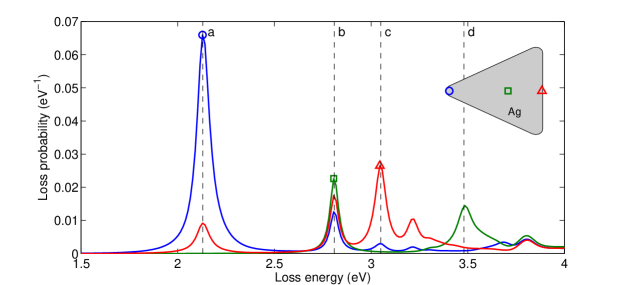
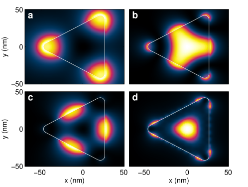
>> demotrianglespectrumat the Matlab prompt, a simulation is performed where the EEL spectra are computed for a triangular silver nanoparticle. The run time is reported in Table 1, and the simulation results are shown in Fig. 2. One observes a number of peaks associated with the different plasmon modes of the nanoparticle. Note that through plot(p,’EdgeColor’,’b’) one can plot the nanoparticle boundary. By running next demotrianglemap.m we obtain the spatial EELS maps at the plasmon resonance energies indicated by dashed lines in Fig. 2. Figure 3(a) reports the map for the degenerate dipolar modes, whereas panels (b–d) show the EELS maps for higher excited plasmon modes (see Ref. [8] for experimental results).
| Demo program | Runtime | Description |
|---|---|---|
| demomie.m | 26.3 sec | Comparison of BEM simulations with analytic Mie results |
| demomiestat.m | 14.7 sec | Same as demomie.m but for quasistatic limit |
| demodiskspectrum.m | 29.4 sec | EEL spectra for nanodisk at selected beam positions |
| demodiskspectrumstat.m | 14.6 sec | Same as demodiskspectrum.m but for quasistatic limit |
| demodiskmap.m | 105.6 sec | Spatial EELS maps for nanodisk at selected loss energies |
| demotrianglespectrum.m | 173.5 sec | EEL spectra for nanotriangle at selected beam positions |
| demotrianglemap.m | 104.6 sec | Spatial EELS maps for nanotriangle at selected loss energies |
2.3 A first example
In the following we briefly discuss the demo file demotrianglespectrum.m (see Sec. 4 for a detailed description of the software). We first set up a comparticle object p for the nanotriangle, which stores the particle boundary and the dielectric materials, as well as a BEM solver bem for the solution of Maxwell’s equations. These steps have been described in some length in a previous paper [29]. Additional information is also provided by the help pages. To set up the EELS simulation, we need the impact parameters of the electron beam, a broadening parameter for the triangle integration (see Sec. 4.1 for details), and the electron velocity in units of the speed of light. Initialization is done through
b = [ - 45, 0; 0, 0; 26, 0 ]; % impact parameters (triangle corner, middle, edge)vel = 0.7; % electron velocity in units of speed of lightwidth = 0.2; % broadening of electron beamexc = eelsret( p, b, width, vel ); % initialize EELS excitationThe exc object returns through exc(enei) the external potentials for a given loss energy, which allow for the solution of the BEM equations by means of artificial surface charges and currents sig [28, 29]. From sig we can obtain the surface and bulk loss probabilities for the electron.
sig = bem \ exc( enei ); % surface charges and currents[ psurf, pbulk ] = exc.loss( sig ); % surface and bulk lossesFinally, the EEL spectrum can be computed by performing a loop over loss energies, and EEL maps can be obtained by providing a rectangular grid of impact parameters. A more detailed description of the EELS classes will be given in Sec. 4.
3 Theory
3.1 Boundary element method (BEM)
For the sake of completeness, we start by briefly summarizing the main concepts of the BEM approach for the solution of Maxwell’s equation (see Refs. [28, 6, 29] for a more detailed discussion). We consider dielectric nanoparticles, described through local and isotropic dielectric functions , which are separated by sharp boundaries . Throughout, we set the magnetic permeability and consider Maxwell’s equations in frequency space [32]. In accordance to Refs. [28, 6, 29], we adopt a Gaussian unit system.
The basic ingredients of the BEM approach are the scalar and vector potentials and , which are related to the electromagnetic fields via
| (1) |
Here and are the wavenumber and speed of light in vacuum, respectively. The potentials are connected through the Lorentz gauge condition . Within each medium, we introduce the Green function for the Helmholtz equation defined through
| (2) |
with being the wavenumber in the medium . For an inhomogeneous dielectric environment, we then write down the solutions of Maxwell’s equations in the ad-hoc form [28, 6]
| (3a) | |||||
| (3b) | |||||
where and are the scalar and vector potentials characterizing the external perturbation. Owing to Eq. (2), these expressions fulfill the Helmholtz equations everywhere except at the particle boundaries. and are surface charge and current distributions, which are chosen such that the boundary conditions of Maxwell’s equations at the interfaces between regions of different permittivies hold. This leads to a number of integral equations. Upon discretization of the particle boundaries into boundary elements, one obtains a set of linear equations that can be inverted, thus providing the solutions of Maxwell’s equation in terms of surface charge and current distributions and . Through Eqs. (3a,b) one can compute the potentials everywhere else. For further details about the working equations of the BEM approach the reader is referred to Refs. [28, 6, 29].
3.2 Electron energy loss spectroscopy (EELS)
In the following we consider the situation where an electron passes by or penetrates through a metallic nanoparticles, and loses energy by exciting particle plasmons. We assume that the electron kinetic energy is much higher than the plasmon energies (for typical electron microscopes operating with electron energies of several hundreds of keV this assumption is certainly fulfilled). We can thus discard in the electron trajectory the small change of velocity due to plasmon excitation, and describe the loss process in lowest order perturbation theory. We emphasize that our approach is correspondingly not suited for low electron energies or thick samples.
For an electron trajectory , with , the electron charge distribution reads
| (4) |
Here and are the charge and velocity of the electron, respectively, is the impact parameter in the -plane, and is a wavenumber. The potentials associated with the charge distribution of Eq. (4) can be computed in infinite space analytically (Liénard-Wiechert potentials [32]), and we obtain [28, 6]
| (5) |
is the modified Bessel function of order zero, and . Within our BEM approach, we can directly insert the expressions of Eq. (5) for the unbounded medium into Eq. (3) since the calculated surface charge and current distributions and will automatically guarantee that the proper boundary conditions at the interfaces are fulfilled [28].
We next turn to the calculation of the electron energy loss. Ignoring the small change of the electron velocity caused by the interaction with the plasmonic nanoparticle, the energy loss can be computed from the work performed by the electron against the induced field [33, 28, 6]
| (6) |
with the loss probability, given per unit of transferred energy,
| (7) |
Note that Eq. (7) is a classical expression, where has been introduced only to relate energy and frequency. is the induced electric field, which can be computed from the potentials originating from the surface charge and current distributions and alone. is the bulk loss probability for electron propagation inside a lossy medium, see Eq. (18) of Ref. [6]. Within the quasistatic approximtion, it is proportional to the loss function and the propagation length inside the medium. Expressions similar to Eq. (7) but derived within a full quantum approach, based on the Born approximation, can be found in Ref. [6].
Quite generally, can be computed by calculating the induced electric field along the electron trajectory and evaluating the expression given in Eq. (7). In what follows, we describe a computationally more efficient scheme. Insertion of the induced potentials of Eq. (3) into the energy loss expression of Eq. (7) yields
| (8) |
Here and are the entrance and exit points of the electron beam in a given medium, and parameterizes the electron trajectory. We next introduce a potential-like term , associated with the electron propagation inside a given medium. Performing integration by parts, we can rewrite the second term in parentheses of Eq. (8) as
The first term on the right-hand side gives, upon insertion into Eq. (8), . The integral expression precisely corresponds to the scalar potential at the crossing points of the trajectory with the particle boundary. As the potential is continuous across the boundaries, the contributions of all crossing points sum up to zero. Thus, we arrive at our final result
| (9) |
In comparison to Eq. (8), this expression has the advantage that the integration is only performed over the particle boundary, where the surface charge and current distributions and are readily available, and we don’t have to compute the induced electric field along the electron trajectory.
3.3 Refined integration over boundary elements
In the calculation of the external potential, Eq. (5), and the EELS probability of Eq. (9) the points where the electron trajectory crosses the boundary have to be treated with care. For small distances, the potential scales with . When integrating this expression within our BEM approach over a small area, we find in polar coordinates that remains finite. The same is true for the surface derivative of the potential.
In a computational approach it is somewhat tedious to perform such integration properly, in particular for crossing points that are located close to the edges or corners of boundary elements. For this reason, we suggest a slightly different approach. The main idea is to replace the Delta-like transversal trajectory profile by a smoothened distribution. The potential at the transverse position then reads
| (10) |
Here [see Eq. (5)] and the term in brackets is our smoothing function, with being a parameter that determines the transversal extension. For small arguments, we can expand , where is the Euler constant, and perform all integrations analytically to obtain . This suggests replacing the potential of Eq. (5) by the smoothened function
| (11) |
For large arguments this expression coincides with the Liénard-Wiechert potential, but remains finite for small arguments. A corresponding smoothening is also performed in the potential-like function of Eq. (9).
3.4 Quasistatic approach
In the quasistaic approximation one assumes that the size of the nanostructure is significantly smaller than the wavelength of light, such that . This allows us to keep in the simulations only the scalar potential and to set in the Green function . We are thus left with the solution of the Laplace or Poisson equation, rather than the Helmholtz equation, but we keep the full frequency-dependence of the permittivities .
The calculation of EELS probabilities with the BEM approach has been described in some detail in Ref. [30]. In the following we briefly describe the basic ingredients. First, we compute the external potential from the solution of Poisson’s equation
| (12) |
with being the charge distribution of Eq. (4). We next compute the surface charge distribution from the solution of the boundary integral equation, which, for a nanoparticle described by a single dielectric function embedded in a background of dielectric constant , reads [30, 29]
| (13) |
Here is the static Green function and denotes the surface derivative, where is the outer surface normal of the boundary. For materials consisting of more than one material, Eq. (13) has to be replaced by a more general expression [29]. Finally, we compute the electron energy loss probability from (see also Eq. (18) of Ref. [30])
| (14) |
where is the bulk loss probability (see Eq. (19) of Ref. [6]).
4 Results and detailed toolbox description
We first discuss the demo file demomie.m that simulates the energy loss probability for an electron passing by a silver nanosphere. Figure 4 shows results of our BEM simulations which are in good agreement with analytic Mie results [6]. Let us briefly work through the demo program.
In the first lines we define the dielectric materials and the nanosphere (for a more detailed discussion of the MNPBEM toolbox see Ref. [29]).
epsm = epstable( ’silver.dat’ ); % metal dielectric functionepstab = { epsconst( 1 ), epsm }; % table of dielectric functionsdiameter = 80; % sphere diameter in nanometers% define nanosphere and dielectric environmentp = comparticle( epstab, { trisphere( 256, diameter ) }, [ 2, 1 ], 1 );We next define the excitation of the electron beam. For the solution of the full Maxwell equations, the excitation and the calculation of the EELS probability is performed by the eelsret class, which is initialized through
exc = eelsret( p, impact, width, vel, ’PropertyName’, PropertyValue, ... )Here p is the previously computed comparticle object, which stores the particle boundaries and the dielectric functions at both sides of the boundary. impact is a vector [x,y] for the impact parameter of the electron beam defined in Eq. (4). If simulations for various impact parameters are requested, as is usually the case for the simulation of EELS maps, impact can also be an array [x1,y1;x2,y2;...]. width is the broadening parameter of the electron beam, see Eq. (11), which will be discussed in more detail below, and vel is the electron velocity to be given in units of the speed of light in vacuum. The optional pairs of property names (’cutoff’, ’rule’, or ’refine’) and values allow to control the performance of the toolbox, as detailed in Sec. 4.1.
In the demomie.m program we next set up the EELS excitation with
b = 10; % minimal distance from nanosphere in nanometersvel = eelsbase.ene2vel( 200e3 ); % electron velocity[ width, cutoff ] = deal( 0.5, 8 ); % width of electron beam and cutoff parameter% electron beam excitation for simulation of full Maxwell equationsexc = eelsret( p, [ diameter / 2 + b, 0 ], width, vel, ’cutoff’, cutoff );Note that eelsbase.ene2vel allows to convert a kinetic electron energy in eV to the electron velocity in units of the speed of light in vacuum . In the above example, a kinetic energy of 200 keV corresponds to a velocity of approximately .
We next set up the solver bemret for the solution of the BEM equations [29] and compute the loss probabilities of Eq. (9) for various loss energies.
bem = bemret( p ); % set up BEM solverene = linspace( 2.5, 4.5, 80 ); % loss energies (in eV)psurf = zeros( size( ene ) ); % initialize array for surface lossesfor ien = 1 : length( ene ) % loop over energies sig = bem \ exc( eV2nm / ene( ien ) ); % surface charges psurf( ien ) = exc.loss( sig ); % EELS loss probabilitiesendHere sig is a compstruct object that stores the surface charges and current distributions and , inside and outside the particle boundaries [28, 29], as computed for the EELS excitation of Eq. (5). With exc.loss(sig) we finally compute the loss probabilities according to Eq. (9). Note that eV2nm defined in units.m allows to convert between energies given in electronvolts and wavelengths given in nanometers, the latter being the units used by the MNPBEM toolbox.

To summarize, in the following we list the most important properties of the eelsret class
exc = eelsret( p, impact, width, vel ); % initializationpot = exc( enei ); % external potentials, see Eq. (5)[ psurf, pbulk ] = exc.loss( sig ); % compute surface and bulk loss probabilitiesWe emphasize that the functionality of the eelsret class is very similar to that of the planewaveret and dipoleret classes, which account for plane wave and dipole excitations. The only major difference is that eelsret requires the particle boundaries p of the comparticle object already in the initialization. This is because upon initialization eelsret computes the crossing points between the particle boundaries and the electron trajectories (if the electron passes by the nanoparticle no crossing points are found), and these crossing points are used in subsequent calculations of the potentials and the loss probabilities to speed up the simulation.
4.1 Electron beam propagation through nanoparticle and EELS maps
We next investigate the situation where the electron beam passes through the nanoparticle. The working principle is almost identical to the previous case where the electron passes by the nanoparticle, but the width parameter and the different optional properties have to be set with more care. In the following, we briefly discuss these quantities in more detail.
-
width. We have discussed in Sec. 3.3 that the integration of the external potentials over the boundary elements can be facilitated if we use a smoothening parameter in the calculation of the external potentials, see Eq. (11). It is important to stress that the integration could be also performed for and that the finite value only facilitates the computation. In general, width should be chosen smaller than the average size of the boundary elements, as also shown in Fig. 5(a).
-
’cutoff’. The
cutoffparameter determines those boundary elements where the external potentials become integrated. In more detail, we select all boundary elements fully or partially located within a circle with radius cutoff and centered around the impact parameter , as shown in Fig. 5(a) by the red circle. cutoff should be set such that at least all direct neighbours of the boundary element crossed by the electron beam are included. -
’refine’ and ’rule’. The integration over the boundary elements is controlled by ’refine’ and ’rule’. refine gives the number of integration points within a triangle. Quadfaces are divided into two triangles. On default
rule=18is used (seedoc triangle_unit_setfor details), and we recommend to use this value throughout. With refine one can split the triangles into subtriangles. Usually the default valuerefine=1should give sufficiently accurate results.
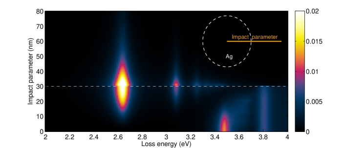
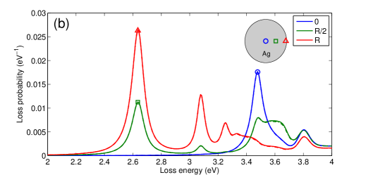
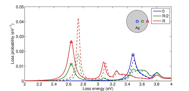
Figure 5(b) shows the EEL spectra of a nanodisk (for parameters see figure caption) for three impact parameters, which are described in the inset. In Fig. 6 we show a density plot of identical loss spectra for a whole range of impact parameters. One observes a number of peaks, attributed to the dipolar and quadrupolar modes at 2.6 eV and 3.1 eV, respectively, a breathing mode at 3.5 eV [14], and the bulk losses at 3.8 eV.
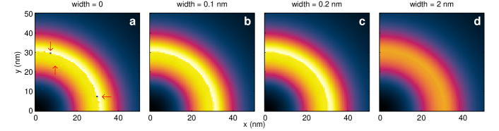
How should one chose the width, cutoff, and refine parameters? Quite generally, the results depend rather unsensitively on the chosen parameters. In Fig. 5 we show results for various width parameters listed in the figure caption, which are almost indistinguishable. In Fig. 7 we depict EELS maps for the dipolar disk mode at 2.6 eV and for various width parameters. For width=0 in panel (a) one observes for certain impact parameters spikes (some of them indicated with arrows), where the loss probabilities becomes significantly enhanced or reduced in comparison to neighbour points. This indicates that the impact parameter is located too closely to the collocation point of the boundary element, and the numerical integration fails. For width parameters of 0.1 or 0.2 nm, panels (b,c), these spikes are absent and the results are almost indistinguishable. Finally, in panel (d) we report results for a too large smoothening parameter with a significant smearing of the features visible in panels (a–c). Thus, width should be chosen significantly smaller than the size of the boundary elements but large enough to avoid spikes in the computed EELS maps.
Let us finally briefly discuss the simulation of EELS maps for a nanotriangle, as computed with the demo program demotrianglemap.m. Results are shown in Fig. 3. First we set up an array of impact parameters and initialize the eelsret object.
% mesh for impact parameters[ x, y ] = meshgrid( linspace( - 70, 50, 50 ), linspace( 0, 50, 35 ) );impact = [ x( : ), y( : ) ]; % impact parametersvel = eelsbase.ene2vel( 200e3 ); % electron velocity[ width, cutoff ] = deal( 0.2, 10 ); % width of electron beam and cutoff parameterexc = eelsret( p, impact, width, vel, ’cutoff’, cutoff );Note that in the initialization of exc we pass a matrix [x(:),y(:)] of impact parameters. As for the BEM solver, we recommend to use for the boundary element integration the same or larger ’cutoff’ and ’refine’ values as for the eelsret object (see Ref. [29] and toolbox help pages for further details).
op = green.options( ’cutoff’, 20, ’refine’, 2 ); % options for face integrationbem = bemret( p, [], op ); % set up BEM solverFinally, once the loss probabilities are computed one should reshape psurf and pbulk to the size of the impact parameter mesh.
p = reshape( psurf + pbulk, size( x ) ); % reshape loss probability
4.2 Electric field and cathodoluminescence
In some cases it is useful to plot the electromagnetic fields induced by the electron beam. We briefly discuss how this can be done. A demo program is provided by demodiskfield.m, and the simulation results are shown in Fig. 8.
We first set up the eelsret object and the BEM solver, following the prescription given above, and compute the surface charge and current distributions.
exc = eelsret( p, [ b, 0 ], width, vel, ’cutoff’, cutoff ); % EELS excitationbem = bemret( p, [], op ); % BEM solversig = bem \ exc( enei ); % surface charges and currentsNext, we define the points where the electric field should be computed, using the compoint class of the MNPBEM toolbox, and define a Green function object compgreen.
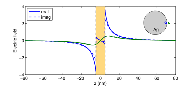
z = linspace( - 80, 80, 1001 ) .’; % z-values for fieldpt = compoint( p, [ b + 0 * z, 0 * z, z ], ’mindist’, 0.1 ); % convert to pointsg = compgreen( pt, p, op ); % Green function objectfield = g.field( sig ); % electromagnetic fields at PT positionse = pt( field.e ); % extract electric fieldIn the last two lines we compute the electromagnetic fields, and extract the electric field. The command e=pt(field.e) brings e to the same form as z, setting fields at points too close to the boundary (which we have discarded in our compoint initialization with the parameter ’mindist’ [29]) to NaN. Figure 8 shows simulation results. For the electron beam passing through the nanodisk, the field amplitude increases strongly in vicinity of the nanoparticle, which we attribute to evanescent plasmonic fields, and is very small inside the nanodisk because of the efficient free-carrier screening inside conductors.
With the MNPBEM toolbox it is also possible to compute the light emitted from the nanoparticles, the so-called cathodoluminescence. To this end, we first set up a spectrumret object for the calculation of scattering spectra, determine the electromagnetic fields at infinity, and finally compute the scattering spectra.
spec = spectrumret; % set up sphere at infinityfield = farfield( spec, sig ); % compute far fields at infinitysca = scattering( spec, field ); % scattering cross sectionIn the initialization of spec one could also use a sphere segment rather than the default unit sphere, e.g., to account for finite angle coverages of photodetectors.
4.3 Parallelization
Efficient parallelization can be achieved for typical energy loops of the form:
for ien = 1 : length( enei ) % loop over energies sig = bem \ exc( enei( ien ) ); % compute surface charges [ psurf( :, ien ), pbulk( :, ien ) ] = exc.loss( sig ); % loss probabilitiesendWe can replace this loop with:
matlabpool open; % open pool for parallel computationparfor ien = 1 : length( enei ) % parallel loop over energies sig = bem \ exc( enei( ien ) ); % same as above ... [ psurf( :, ien ), pbulk( :, ien ) ] = exc.loss( sig );endThe important point is that all computations inside the loop can be performed independently, as is the case for the BEM simulation as well as the calculation of the external potentials and loss probabilities.
4.4 Quasistatic limit
The implementation of the quasistatic limit within the eelsstat class closely follows the retarded case. The demo program demodiskspectrumstat.m is very similar to demodiskspectrum.m discussed in Sec. 4.1. We first set up a disk-like nanoparticle and specify the electron beam parameters. Next, we initialize an eelsstat object by calling
exc = eelsstat( p, b, width, vel, ’cutoff’, cutoff, ’refine’, 2 ); % EELS excitationThe definition of the various parameters is identical to the retarded case. Finally, we set up the quasistatic bemstat or bemstateig BEM solver [29], and compute the surface charge distribution and the energy loss probability using the equations presented in Sec. 3.4
bem = bemstat( p, [], op ); % set up quasistatic BEM solverfor ien = 1 : length( enei ) % loop over energies sig = bem \ exc( enei( ien ) ); % compute surface charge [ psurf( :, ien ), pbulk( :, ien ) ] = exc.loss( sig ); % electron energy loss probabilityendSimulation results are shown in Fig. 9. We observe that the results of the full and quasistatic simulations are very similar, and only for the dipolar mode at lowest energy the peak position and width somewhat differ due to retardation effects and radiation damping
Acknowledgment
I am grateful to Andi Trügler for most helpful discussions, and thank him as well as Toni Hörl, Jürgen Waxenegger, and Harald Ditlbacher for numerous feedback on the simulation program. This work has been supported by the Austrian Science Fund FWF under project P24511–N26 and the SFB NextLite.
References
- [1] S. A. Maier, Plasmonics: Fundamentals and Applications, Springer, Berlin, 2007.
- [2] H. Atwater, Scientific American 296(4) (2007) 56.
- [3] J. A. Schuller, E. S. Barnard, W. Cai, Y. C. Jun, J. S. White, M. L. Brongersma, Nature Mat. 9 (2010) 193.
- [4] M. I. Stockman, Optics Express 19 (2011) 22029.
- [5] L. Novotny, B. Hecht, Principles of Nano-Optics, Cambridge University Press, Cambridge, 2006.
- [6] F. J. Garcia de Abajo, Rev. Mod. Phys. 82 (2010) 209.
- [7] M. Bosman, V. J. Keast, M. Watanabe, A. I. Maaroof, M. B. Cortie, Nanotechnology 18 (2007) 165505.
- [8] J. Nelayah, M. Kociak, O. Stephan, F. J. Garcia de Abajo, M. Tence, L. Henrard, D. Taverna, I. Pastoriza-Santos, L. M. Liz-Martin, C. Colliex, Nature Phys. 3 (2007) 348.
- [9] J. Nelayah, L. Gu, W. Sigle, C. T. Koch, I. Pastoriza-Santos, L. M. Liz-Martin, P. A. van Anken, Opt. Lett. 34 (2009) 1003.
- [10] B. Schaffer, W. Grogger, G. Kothleitner, F. Hofer, Ultramicroscopy 110 (2010) 1087.
- [11] B. Schaffer, U. Hohenester, A. Trügler, F. Hofer, Phys. Rev. B 79 (2009) 041401(R).
- [12] O. Nicoletti, M. Wubs, N. A. Mortensen, W. Sigle, P. A. van Aken, P. A. Midgley, Optics Express 19 (2011) 15371.
- [13] D. Rossouw, G. A. Botton, Phys. Rev. Lett. 110 (2013) 066801.
- [14] F.-P. Schmidt, H. Ditlbacher, U. Hohenester, A. Hohenau, F. Hofer, J. R. Krenn, Nano Letters 12 (2012) 5780.
- [15] S. Mazzucco, Geuquet, J. Ye, O. Stephan, W. Van Roy, P. Van Dorpe, L. Henrard, M. Kociak, Nano Lett. 12 (2012) 1288.
- [16] W. Sigle, J. Nelayah, C. Koch, P. van Aken, Optics Letters 34 (2009) 2150.
- [17] M. W. Chu, V. Myroshnychenko, C. H. Chen, J. P. Deng, C. Y. Mou, J. Garcia de Abajo, Nano Lett. 9 (2009) 399.
- [18] M. N’Gom, S. Li, G. Schatz, R. Erni, A. Agarwal, N. Kotov, T. B. Norris, Phys. Rev. B 80 (2009) 113411.
- [19] A. L. Koh, K. Bao, I. Khan, W. E. Smith, G. Kothleitner, P. Nordlander, S. A. Maier, D. W. McComb, ACS Nano 3 (2009) 3015.
- [20] A. L. Koh, A. I. Fernandez-Dominguez, D. W. McComb, S. A. Maier, J. K. W. Yang, Nano Lett. 11 (2011) 1323.
- [21] F. J. Garcia de Abajo, M. Kociak, Phys. Rev. Lett. 100 (2008) 106804.
- [22] U. Hohenester, H. Ditlbacher, J. Krenn, Phys. Rev. Lett. 103 (2009) 106801.
- [23] G. Boudarham, M. Kociak, Phys. Rev. B 85 (2012) 245447.
- [24] A. Hörl, A. Trügler, U. Hohenester, Phys. Rev. Lett. 111 (2013) 086801.
- [25] N. Geuquet, L. Henrard, Ultramicroscopy 110 (2010) 1075.
- [26] N. W. Bigelow, A. Vaschillo, V. Iberi, J. P. Camden, D. J. Masiello, ACS Nano 6 (2012) 7497.
- [27] V. Myroshnychenko, J. Rodriguez-Fernandez, I. Pastoriza-Santos, A. M. Funston, C. Novo, P. Mulvaney, L. M. Liz-Marzan, F. J. Garcia de Abajo, Chem. Soc. Rev. 37 (2008) 1792.
- [28] F. J. Garcia de Abajo, A. Howie, Phys. Rev. B 65 (2002) 115418.
- [29] U. Hohenester, A. Trügler, Comp. Phys. Commun. 183 (2012) 370.
- [30] F. J. Garcia de Abajo, J. Aizpurua, Phys. Rev. B 56 (1997) 15873.
- [31] P. B. Johnson, R. W. Christy, Phys. Rev. B 6 (1972) 4370.
- [32] J. D. Jackson, Classical Electrodynamics, Wiley, New York, 1999.
- [33] R. H. Ritchie, Phys. Rev. 106 (1957) 874.