Nodal “ground states” and orbital textures in semiconductor quantum dots
Abstract
Conventional understanding implies that the ground state of a nonmagnetic quantum mechanical system should be nodeless. While this notion also provides a valuable guidance in understanding the ordering of energy levels in semiconductor nanostructures, there are reports that nodal ground states for holes are possible. However, the existence of such nodal states has been debated and even viewed merely as an artifact of a model. Using complementary approaches of both and tight-binding models, further supported by an effective Hamiltonian for a continuum model, we reveal that nodal ground states in quantum dots are not limited to a specific approach. Remarkably, the emergence of nodal hole states at the top of the valence band can be attributed to the formation of orbital vortex textures through competition between the hole kinetic energy and the coupling to the conduction band states. We suggest an experimental test for our predictions of the reversed energy ordering and the existence of nodal ground states. We discuss how our findings and the studies of orbital textures could be also relevant for other materials systems.
I Introduction
Unlike the common expectation that a bound state of a particle should be nodeless,Marder:2010 ; Snoke:2008 ; Gywat:2010 theoretical calculations in semiconductor quantum wiresPersson2006:PRB and quantum dotsBagga2003:PRB ; Bagga2005:PRB ; Bagga2006:PRB ; Yu2003:JPC (QDs) have predicted hole ground states with a node. Those ground states occur with the inversion of the energy level ordering between nodeless (-like) and nodal (-like) wavefunctions due to various factors, such as the confinement size and strength, the choice of a material, and the spin-orbit interaction. This peculiar phenomenon is connected to the formation of dark excitons that exhibit very long recombination time and Stokes shiftEfros1995:PRL ; Efros1996:PRL ; Bagga2006:PRB in the luminescence of InAs and CdSe QDs. One can expect that such nodal states would also have intriguing implications for magnetically-doped QDs and provide additional control for their magnetic ordering.Seufert2001:PRL ; Besombes2004:PRL ; Leger2005:PRL ; Henneberger:2010 ; Fernandez-Rossier:2011 ; Beaulac2009:S ; Xiu2010:ACSN ; Bussian2009:NM ; Sellers2010:PRB ; Fernandez2004:PRL ; Zhang2007:PRB ; Govorov2005:PRB ; Abolfath2008:PRL ; Oszwaldowski2011:PRL ; Pientka2012:PRB In this work we show how the presence of the nodal ground state is associated with the emergence of orbital textures that minimize the energy of underlying model we use to describe QDs.
While there appeared some criticism asserting that the existence of nodal ground state is just a theoretical artifact,Fu1997:APL ; Wang1998:JPCB ; Wang2000:APL a systematic effort to either prove or disprove the occurrence of the level ordering inversion between the nodal and nodeless states is still missing. In fact, one is tempted to invoke different arguments to dismiss the occurrence of such nodal ground states. Elementary understanding of quantum mechanics would suggest that the nodeless state and thus minimization of the kinetic energy should be preferred. A similar reasoning would follow from the Sturm-Liouville theorem for differential equations.Morse:1953
However, a closer look at the character of the hole ground state displays more complexities, which prevent us from simply concluding that a nodal wavefunction cannot describe the ground state. The hole ground state is not a “true” ground state, but a state in the middle of the whole spectrum of single-particle energy levels. The hole represents a lack of an electron, the ground state of hole refers to the highest energy state in the valence band (VB) in the electronic energy dispersion. Additionally, the corresponding Hamiltonian describes multiband wavefunctions arising from the band structure as shown in Fig. 1(a). Therefore, the hole ground state with a nodal wavefunction is not forbidden.

Even if the suggested nodal ground states are not impossible, are the methods employed to identify them indeed appropriate? Specifically, their identification relies on the use of a model which is commonly employed to describe the band structure in bulk semiconductors. The model is based on an effective Hamiltonian with periodic Bloch functions as its solutions which, for a certain crystal momentum , form a complete set. Near a specific (typically -point, ) an accurate band structure is obtained perturbatively.Yu:2010
Several qualitative features arising from a model applied to diamond or zinc-blende semiconductors, such as the opening of the energy gap, , and the VB structure are illustrated in Fig. 1(a). In the VB, the heavy and light holes are separated by the spin-orbit gap, , from the split-off band. The versatility of the model was successfully used to elucidate a wealth of phenomena in semiconductors and their nanostructures, including optical properties,Winkler:2003 ; Gywat:2010 ; Meier:1984 ; Dyakonov:2008 ; Drouhin2008:PRB the spin Hall effect, Murakami2003:S topological insulators,Hasan2010:RMP and Zitterbewegung.Bernardes2007:PRL While a model with an envelope function approximation is also frequently applied to low-dimensional systems, such as quantum wells, wires, and dots,kdotp ; Winkler:2003 ; Gywat:2010 sometimes it is more challenging to justify its validity.
A complementary picture to examine the occurrence of the nodal ground states can be obtained from a tight-binding (TB) model. Unlike the model, one can consider an electron in a solid as localized within an isolated atom placed at each lattice site. If no interaction between neighboring atoms exists, there are degenerate energy levels corresponding to - and -orbitals, shown on the left in Fig. 1(b). In a realistic solid, since atoms are not completely isolated, an electron at one site interacts with the neighboring atoms. In a TB model, electronic wavefunction in the primitive unit cell can be approximated by a linear combination of atomic orbitals (LCAO) of isolated atoms at different sites. If we next consider hopping among - and -orbitals, bonding and antibonding states will form, Fig. 1(b), middle. Finally, when we introduce - coupling, the semiconducting gap opens in the bulk. Such an atomistic TB model provides a different approach to study semiconductor nanostructures in which the model may not capture the full symmetry of atomic wavefunctions, and it could help our microscopic understanding of the level ordering in a QD.
We combine these two complementary models to systematically explore the presence of nodal ground states and to eliminate the possibility that our results are an artifact of a specific method. Within both and TB models we predict an unconventional level ordering in which the nodal (-like) wavefunction can attain an energy lower than the nodeless (-like) wavefunciton. This departure from the conventional nodeless ground state can be understood even from a simple TB description and we can attribute it to mixing between orbitals of different types centered at different atomic sites. We also develop an effective Hamiltonian from the continuum limit of a TB model which explains how the emergence of nodal ground state is related to the orbital ordering and the formation of orbital textures. Throughout this paper, uppercase (lowercase) letters , (,) refer to envelope functions (atomic orbitals).
Our presentation is organized as follows. After this Introduction, in Sec. II we provide some background about the model and its parameters. We then describe the phase diagram for the occurrence of a nodal ground state. In Sec. III we describe several TB models in both two and three dimensional crystal structures and identify the microscopic origin of the nodal ground state. In Sec. IV we discuss several implications of our findings and propose an experiment which could be used to probe the presence of nodal ground states in QDs. Our conclusions provide the main findings of this work as well as the possible future directions.
II Model
Formulation of a bulk model can vary significantly in its complexity, the choice of the specific system, and the number of bands included. For transparency, we focus on its main features in a simple implementation of the non-interacting single electron picture. Invoking the Bloch theorem, , we obtain an effective Schrödinger equation for Bloch functions
| (1) |
with and , where is the the band index, momentum operator, the Bloch function has the periodicity of the lattice potential , and is the free electron mass. If and are known at point, can be treated as a perturbation in terms of suggesting that for QDs, the model should work better for larger systems where is smaller. To some extent, this limitation can be removed by using a large number of bands so that the bulk model accurately reproduces the band structure over the whole Brillouin zone. However, there is only a limited number of experimentally determined energy gaps and matrix elements which are needed as the input to the model.Yu:2010
We begin by considering a reduced Hilbert space that consists of heavy hole (HH) and light hole (LH) bands. The perturbative procedure leads to the Luttinger Hamiltonian,Luttinger ; Winkler:2003 ; Yu:2010 given in terms of the Kohn-Luttinger parameters , , and . The standard procedure for confined systems,Winkler:2003 i.e., the replacement , leads to
| (2) |
where is the angular momentum operator, and stands for cyclic permutations. Each set of , , represents a specific material, and several examples are given in Table 1. The four-band model of Eq. (2) corresponds to limit and we often employ the spherical approximation in which both and are replaced byGywat:2010 ; Baldereschi1973:PRB
| (3) |
This approximation suppresses the warping (anisotropy) of Fermi surface in the bulk and the effective masses are then and .Gywat:2010 VB energy levels for QDs can be calculated by diagonalization of Eq. (2) expressed in a suitably chosen basis in -space for the envelope functions.note2 We consider a cubic domain of dimensions with zero boundary conditions unless explicitly mentioned otherwise. The cubic geometry simplifies the comparison between and TB models, however, choosing a different confinement geometry, e.g., spherical or cuboid (see Appendix D) confinement, does not change qualitatively our findings, as long as the geometry is highly symmetric.
| Material | (meV) | ||||
|---|---|---|---|---|---|
| GaAs | 6.85 | 2.10 | 2.90 | 341 | 0.377 |
| InAs | 20.40 | 8.30 | 9.10 | 380 | 0.430 |
| CdTe | 5.30 | 1.70 | 2.00 | 949 | 0.355 |
| Ge | 13.38 | 4.24 | 5.69 | 290 | 0.382 |
The four-band model described by Eq. (2) can be generalized to six bands by including two split-off bands of the VB and spin-orbit interaction
| (4) |
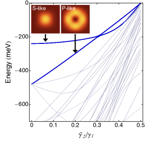
where and are spin and orbital angular momentum operators, and is the splitting shown in Fig. 1(a). Instead of the matrix in Eq. (2), we then use standard six-band model as in Eq. (A8) from Ref. Abolfath2001:PRB, with replaced. In the limit , the spin-orbit coupling effects are eliminated, and the 6 6 Luttinger Hamiltonian can be parameterized by the ratio and once the spherical approximation is invoked. Cubic QD energy levels are plotted in Fig. 2 as a function of this parameter which simulates a continuous variation of the material in terms of and . In the opposite limit of , our Hamiltonian recovers analogous results, such as Fig. 2 of Ref. Vyborny2012:PRB, which is obtained with four-band model.note:sign We find a crossing between two types of ground states as increases and it occurs well before the upper limit of is reached. Larger values of correspond to materials with small and the upper limit maps to .
Both energy levels shown by bold lines in Fig. 2 are sixfold degenerate and their envelope functions modulus squared is shown in the upper part of the figure. These results imply that, in contrast to the common notion, the topmost energy level in the VB can be the -like state with a node rather than the -like state without a node. The crossing between these two states occurs at approximately . Below this value, -like states are at the top of the VB above the -like states and this ordering is reversed as increases. Similar behavior is found in spherical QDs.Yu2003:JPC In the following, we discuss materials in which the reversed ordering may occur.
While the ratio is important, it is not the only factor that determines the ordering of the two uppermost states. The crossing of the - and -like states also depends on other factors, such as the strength of spin-orbit coupling, the depth and shape of the confinement, and the presence of interfacial and surface QD states. Even if we employ the spherical approximation of Eq. (3), there are several parameters on which the energy level ordering depends. We discuss the influence of , and on the topmost VB level wavefunction character in Fig. 3. The color code indicates the (squared) weight of the unperturbed -like wavefunction,note2 in the darker areas the -like states are closer to the band edge than -like states.
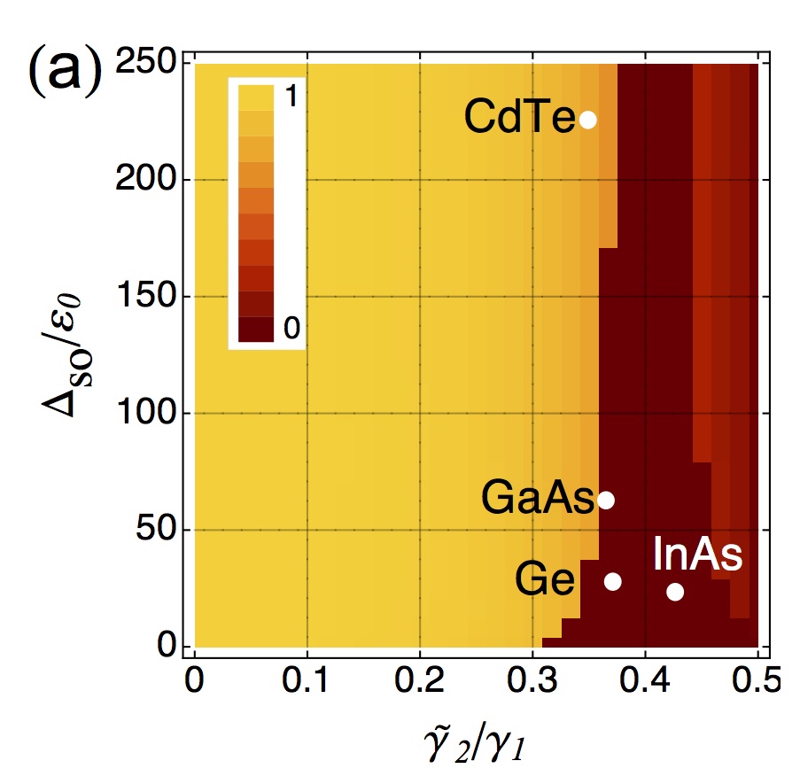
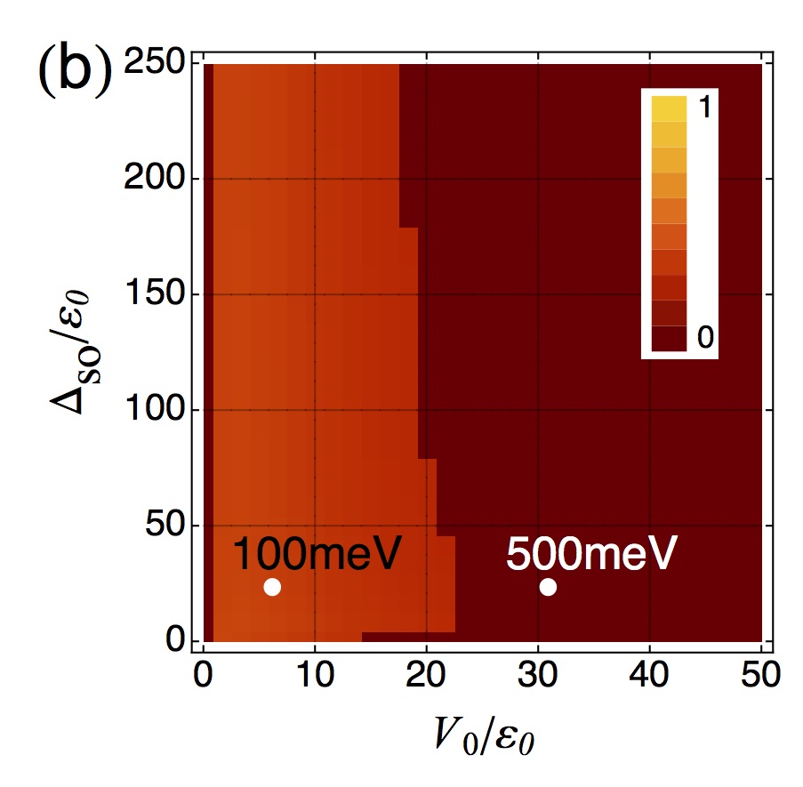
In Fig. 3(a) we assume an infinitely deep confinement, arguably a good approximation for colloidal QDs.Gywat:2010 Around there is a window of the reversed ordering of states, favoring -like ground state. Materials such as InAs, GaAs and Ge within this range are expected to demonstrate the reversed ordering. An increase in the normalized spin-orbit coupling, appears detrimental to the -like ground state. Because of this reason, the well-established material for single-QD optical experiments, CdTe, misses the range of reversed level ordering. However, its relatively large value of could still be compensated for by smaller dimensions of the QD, since the ordering depends on . We also examine the influence of the finite confinement depth in Fig. 3(b) and consider a well-in-a-well structure. For this panel, we use InAs parameters given in Table 1 with and include a piecewise constant potential in our total Hamiltonian.note2 The marked points are labeled by their confinement depths corresponding to a InAs QD with nm. While deeper confinement makes the reversed ordering more likely, at a fixed effective depth an increase in the spin-orbit coupling can promote -like ground state, in contrast to what was shown for infinite confinement in Fig. 3(a). These dissimilar trends suggest that the interface between the QD and the surrounding material or vacuum can alter the ordering of - and -like states.
We conclude this account of the model and its results by recalling that several assumptions,kdotp ; Gywat:2010 ; Yu:2010 such as the smoothness of the confinement potential (on the atomic scale) and sufficiently small values involved in the wavefunctions may have not been fully satisfied in a rigorous manner. It may then be rather puzzling that a model can provide a good agreement with experiments,Gywat:2010 even when its validity is unclear.
III Tight-Binding (TB) Model
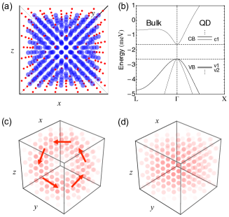
To scrutinize the relevance of the -like ground state, obtained in Section II using model, it is important to examine if such findings will be preserved within a different framework. In atomistic TB models, abrupt interface between the QD material and vacuum is introduced naturally. No special boundary conditions need to be considered although we still need to pay attention to QD termination and passivation. Guided by the phase diagram obtained from the model in Fig. 3(a), we now turn to an idealized TB model for Ge QD to test the possibility for the -like ground state. Our results, illustrated in Fig. 4, reveal that such a nodal state indeed appears at the top of the VB and is associated with an orbital texture. In order to understand the origin of the reversed ordering of energy levels, we discuss TB models on simpler crystal lattices such as a two-dimensional (2D) square lattice in Sec. III A. We then identify the hybridization between - and -orbitals on neighboring atomic sites as the driving mechanism for the ordering reversal, construct a continuum model which renders this mechanism clearly understandable and return to the more realistic TB models to confirm that this mechanism leads to results as shown in Fig. 4.
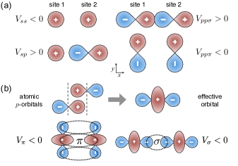
Our TB models consider only the nearest-neighbor hopping with one - and three -orbitals at each atomic site. Since model in the previous section shows that the spin-orbit interaction does not promote the occurrence of the -like ground state — it even tends to suppress it — we assume it absent, which would correspond to in the notation of Sec. II. The spin-up and spin-down states are then degenerate and we can focus on one of them only. The TB model is parametrizedYu:2010 by the and -orbital on-site energies, , , where , and four hopping parameters between the nearest-neighbors , , , and , where is the full Hamltonian, is the lattice site, is the distance between nearest-neighbors. Note that is a unit vector along [100] direction, not an operator. These definitions of hopping parameters are illustrated in Fig. 5(a). In accordance with Slater-Koster rules (see Table 2), the most general TB Hamiltonian we use in this paper can be written as,
| (5) | |||||
where is a vector pointing from to the nearest-neighbors, and is -orbital state at site . is the on-site energy of -orbital, while are dependent energy integrals between - and -orbitals separated by .
| = | ||
| = | ||
| = | ||
| = | ||
| = | ||
| = |
Based on our calculations in Fig. 3, we chose a diamond-structure germanium QD to search for a -like state at the top of the VB. Having found parameters of the passivation layer to avoid surface states (see Sec. III C and Appendix C), we show in Fig. 4(c,d) that the two topmost states are indeed -like and -like, bearing resemblance to the model results. The QD considered consists of total of 512 atomic sites, including the passivation layer atoms shown by smaller red dots in Fig. 4(a). The QD energy levels are shown together with the bulk band structure in Fig. 4(b) and we can see that the -like state lies above the -like state. We defer the detailed description of our Ge QD model to Sec. III C and proceed to analyze simplified TB models that also show the reversal of energy level ordering.
III.1 Square lattice
A square lattice provides a simple TB model that still contains the reversed level ordering. The transparency of this approach allows us to develop an intuitive understanding of the origin of the reversed level ordering and to further support it using an effective Hamiltonian for a continuum model. We consider a square lattice of by atomic sites and express all parameters of the ensuing -dimensional Hamiltonian matrix in terms of
| (6) |
-orbitals are assumed to be decoupled from the other orbitals and are disregarded. By choosing , , , and , we obtain bulk band structure of this 2D crystal that is analogous to that of a 3D zinc-blende semiconductor. The equal sign of the - and -bond hopping parameters can be understood from the analogous situation of effective -, -orbitals described in Fig. 5(b). These effective orbitals can be considered as basis for the VB states that comprise the bonding -orbitals, while conduction band (CB) states arise from the antibonding -orbitals. However, for clarity of the description of our model, we keep the representations of simple atomic orbitals shown in Fig. 5(a) without losing generality of our results.
Turning our attention to confined systems, we look for the eigenfunctions in the form of linear combination of atomic orbitals,
| (7) |
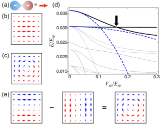
where is the -orbital. The coefficients can be understood as the multi-component envelope function and is the probability of an electron being at the site in the given state. Examples of this probability in the -like and -like states in 3D diamond lattice system are shown in Fig. 4(c,d). To analyze the wavefunctions on a 2D square lattice, it is useful to introduce the following basis
| (8) |
where the positive integers and can be understood as the quantum numbers for the envelope functions, corresponds to lattice point position and is the lattice constant. For , the TB Hamiltonian in Eq. (5) can be diagonalized exactly, yielding the usual sequence of CB states, starting with , , , and . Here, using the notation from Eq. (8), the states are ordered by increasing energy, and indicate degenerate states. For an increasing hole energy, going down from the top of the VB, the sequence begins with and , i.e., a conventional ordering of energy levels with the -like hole ground state (twofold degenerate) and the -like first excited states (fourfold degenerate). There is no coupling between VB and CB states in this simple case.
In Fig. 6 we show the evolution of the energy levels with the hopping parameter for a square lattice with 36 atoms. Once - hybridization is included (), the VB and CB states start to couple with each other leading to level repulsion and removal of some degeneracies. As the increases, -like states are pushed down by CB levels and -like states split into four levels (with ). For a sufficiently large hopping parameter, , one of these -like states crosses the -like manifoldnote1 and becomes the hole ground state. Remarkably, over the range of displayed values, this state is nearly independent of in stark contrast with all the other states shown in Fig. 6(d). These numerical results are further corroborated by the perturbation theory for the two lowest states at (dashed lines).
What is the origin of the -like hole state insensitivity to ? How can we interpret an unconventional ordering of the energy levels at the top of the VB? To elucidate this puzzling behavior we introduce a simple vector representation for an individual atomic -orbitals, shown in Fig. 6(a). We assign an arrow to represent as a vector, recalling Eq. (7). In this representation we can intuitively associate the VB level ordering with the formation of corresponding orbital textures. One of the -like states is described by the orbital texture shown in Fig. 6(b), the other has the same texture rotated by . The -like state shown in Fig. 6(c), on the other hand, exhibits a vortex in the orbital texture. This state, orbital vortex state (OVS), is distinguished among four degenerate -like states at . It consists of -like states with collinear wavefunctions as shown in Fig. 6(e), indicating that the OVS wavefunction is approximatelly up to normalization. Analysis of the actual wavefunction (besides the orbital textures), confirms this conclusion as we describe below. We now derive a continuum approximation of our TB model which explains why the vortex state in the orbital texture is less sensitive to the - hybridization than the -like state in Fig. 6(b).
We focus on the states at the top of the VB and take the - hybridization as a weak perturbation, the small parameter being . The TB Hamiltonian downfolded into the subspace of -, -orbitals reads
| (9) |
The projection operator to the , subspace is denoted by and is the part of the TB Hamiltonian proportional to . We also assume that the VB and CB band widths are small compared to . We write as
| (10) |
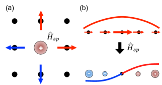
with the lattice sites, the nearest neighbor vectors, index for -orbitals, and for Hermitian conjugate. The direction cosine of is written as in accordance with Slater-Koster rules (see Table 2). Equation (10) is visualized in Fig. 7(a). Due to the direction cosine , hopping from a site to adjacent sites gives opposite signs to the resultant atomic orbitals, and this can be approximated as a derivative operator to the envelope function in the continuum limit. Applying the general form of a wavefunction containing only - and -orbitals
| (11) |
to defined by Eq. (9), we obtain (see Appendix A for details)
| (12) |
Assuming slow variations of the wavefunction at the atomic length scale, we can make the continuum approximation,
| (13) |
We represent the wavefunction from Eq. (11) as a vector field . The two components in refer to wavefunctions in the -orbital space and its divergence term is defined as . An equation analogous to Eq. (13) can be found for .
By replacing discrete lattice points by an integral over , we arrive at , the continuum Hamiltonian projected to the -orbital subspace,
| (14) |
The first term is the usual TB kinetic energy that accounts only for the -orbital part of the wavefunction and the second term reflects the effect of -orbital admixtures. It is a negative (positive in hole representation) divergence term that penalizes certain orbital textures. For a texture as in Fig. 6(b), where all vectors are mutually parallel, the zero boundary conditions imply that vector lengths must change along the ‘streamlines’ causing a large value of . On the other hand, the vortex orbital texture in Fig. 6(c) allows to combine a small value of the divergence term in Eq. (14) with the boundary conditions satisfied. At the same time, this texture requires that there be a node in the center of the QD so that divergent kinetic energy (first term) in Eq. (14) is avoided. Hence the OVS becomes the topmost state in the VB at large enough values of . By construction, the divergence term only occurs with multicomponent wavefunctions that can be represented by a vector field (orbital texture) while single-component wavefunctions such as the CB states have the usual -like ground state. Details on the continuum model are given in Appendix A.
This intuitive understanding of insensitivity of OVS based on continuum limit can be confirmed in the discrete square lattice TB model. Also in second order perturbative calculation with respect to , analytical expressions can be obtained for the discrete lattice, and we will show below with Eq. (20) that both results precisely match. Results of this calculation are shown by the dashed lines in Fig. 6(d). Although we do not expect the perturbative calculation to give quantitatively precise value of , the difference from the full (non-perturbative) TB calculation is not very large. The unperturbed wavefunctions of the -like states are
| (15) |
and the four degenerate () -like states are
| (16) |
up to normalization. Since of Eq. (9) is symmetric to inversion both in the and directions, we can straightforwardly derive coupling rules between the VB and CB such as
| (17) |
Carrying out the degenerate-level perturbative calculation, we find that the degenerate -like VB levels split into four states, and the OVS is written as,
| (18) |
Owing to the coupling rules of Eq. (17), we immediately find . To show that OVS is the most weakly coupled state of the four -like states, it is necessary to mention that the coupling strength decreases with high values of (see Appendix. E). The lowest CB state to which OVS couples is and the corresponding matrix element of is small for this state. On the other hand, a relatively large value of leads to the strong coupling of the -like state with the CB state, and to the band repulsion that makes the -like state energy drop quicker than the OVS with increasing as seen in Fig. 6(d).
In the limit the energy level reversal can be analyzed quantitatively using
which denote the energy level shift of the -like states and the OVS, respectively. Note that the complete expression for energy is and , where are the energies at . In the limit of an infinite number of atoms we get
| (20) |
implying that the level repulsion from the CB levels is stronger for the -like states as we have argued so far. Identical result to Eq. (20) is derived within continuum model and is shown in Eqs. (A-12) and (A-13) in Appendix A. The energy of the -like state will therefore eventually drop below the one of the OVS, provided we stay in the perturbative regime for accordingly large values of . Full model calculations in Fig. 6(d) show that the crossing indeed occurs.
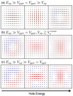
While the reversal of the energy level ordering occurs, - hybridization promotes the modification of orbital textures of - and -like states as well. Evolution of orbital textures as a function of is shown in Fig. 8, with each row belonging to three topmost levels of the VB for different TB parameter regimes, the top level states being always on the left. This figure contains results of the full TB model calculation. In Fig. 8(a), the states are ordered as , and OVS in the regime of before the - level crossing in Fig. 6(d). After the - level crossing occurs for larger , the -like state becomes the ground state and the -like states get appreciable admixtures from other basis states of Eq. (8) as it can be seen in Fig. 8(b). The original -like state is gradually modified so that the divergence of the orbital texture is decreased, i.e., the alignment or the “streamline” of arrows acquires non-zero curvature as increases. As increases further that , in Fig. 8(c), the divergence term in the continuum Hamiltonian of Eq. (14) becomes much more important than the - kinetic energy, and we approach a different limit in which the divergence of the texture becomes zero. Due to this zero divergence, the -dependence in energy vanishes in the large limit, as shown in Fig. 6(d). The -like state remains as the ground state (see Appendix A for its explicit expression of the wavefunction), while the curvature in the -like states in (b) develops into a vortex-anti-vortex texture, with opposite winding numbers. The vortices are gradually introduced into -like states through the boundary of the finite sample, as we go from (b) to (c).
III.2 Simple cubic and face centered cubic structure
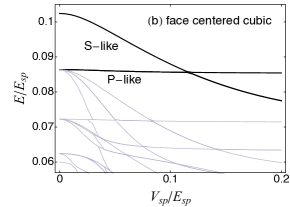
Before we proceed to TB models of the actual semiconductor materials (in our case, diamond structure), we consider two 3D models as an intermediate step. 3D models include also -orbitals on each atomic site and the 2D basis of Eq. (8) can be generalized to , . The most straightforward extension of the 2D square lattice is a 3D simple cubic (SC) lattice. Both square and SC lattice lead to mutually analogous results. Levels at the top of the VB, shown in Fig. 9(a) as a function of , closely resemble those of Fig. 6(d) but the degeneracies are different. There are now three degenerate -like states, a trivial consequence of different dimensionality, written as
| (21) |
in the limit. In contrast to the square lattice, the OVS is no longer non-degenerate and its manifold is spanned by
| (22) |
emerging from ninefold degenerate -like states in the limit. The perturbative analysis that led us to Eq. (III.1) in the case of the square lattice can be carried out analogously and we find, for example, the -like state couples strongly to the CB state. On the other hand, the OVSs couple much more weakly to the CB, owing to the high values of , , involved just as it was the case for the square lattice. For example, couples first to no lower state than in the CB (see discussion in Appendix E).
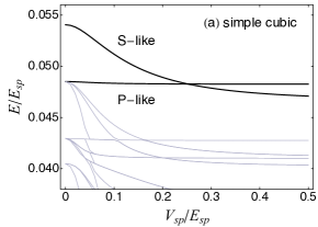
The bulk four-band SC model can be downfolded into an effective Hamiltonian as it is explained in detail in Appendix B. This mapping allows to link the Kohn-Luttinger parameters of the model to the TB parameters by comparing the band curvatures in the -point and it leads to
| (23) |
where is defined in Eq. (B-11). If we insert the parameters of the calculation in Fig. 9(a) together with , we obtain . This value falls into the OVS region in Fig. 3(a), demonstrating a correspondence between the TB and models.
Similar results are obtained for the FCC model, the notable difference being a somewhat smaller value of which can be seen in Fig. 9(b). The FCC model is the closest to the atomistic model of a zinc-blende or diamond-structure material with the restriction imposed that each primitive unit cell is described by a single effective atomic site. The reversed level ordering at the top of the VB clearly stems from the - hybridization in this model and it can be intuitively understood on the basis of the continuum model of Eq. (14). In the next subsection, we discuss the subtleties of lifting the mentioned restriction and the move towards a more realistic model of the QD.
III.3 Diamond structure
In the case of the diamond lattice (equivalent to the zinc-blende lattice with anions replaced by the same element as cations), there are the antibonding combination of the two -orbitals and the bonding combinations of , , that form the bottom of the CB and the top of the VB, respectively, as schematically shown in Fig. 1(b). Such an effective model was the starting point for the calculations of the preceding subsection. The ordering of the on-site energies with is a consequence of them being specific effective orbitals belonging to a pair of atoms rather than actual atomic - and -orbitals (recall Fig. 5). From the overall perspective of the bulk band structure implied by this effective model, the role of is rather minor, and more importantly, this parameter is not responsible for the formation of the gap between CB and VB. This role was assigned to .
The diamond or zinc-blende lattice eight-band TB models (spin is still disregarded) is substantially different, i.e., the gap opens primarily due to - hybridization as illustrated in Fig. 1(b). We will show that the - hybridization retains its effects that were discussed with the simpler models (see Fig. 6 and 9) also in diamond structure, but the value of has to be kept large enough so that the gap opens in the bulk band structure. In other words, it does not make sense to consider the limit in diamond structure, because the bulk band structure will not even have a band gap in such limit. For confined systems, couplings between the individual bands are altered and this -related “gap-forming” mechanism may fail which can manifest itself in the formation of midgap states. Both spuriousJaskolski2001:Vac and physicalHapala2013:PRB midgap states have been discussed in the literature.Winkler:2003 The latter one can be avoided by suitable passivation of the QD surface, for example by covering the QD surface by a layer of hydrogen atoms.
We focus on germanium as a material with diamond lattice guided by the calculations in Fig. 3. We use the bulk TB model parameters , , , which consider only nearest-neighbor interactions Chadi1975:PTSb (see Appendix B). Realistic effective masses are obtained for the bulk band structure with , but this simplified model with nearest-neighbor interactions predicts too high CB energy at -point in the Brillouin zone, and therefore, it fails to reproduce the indirect band gap in natural germanium. A 344-atom (14-atomic-layer) QD of approximately cubic shape is first constructed from Ge atoms shown as larger blue dots in Fig. 4(a). Then, the whole structure is covered by an extra “passivation layer” of distinct atoms (smaller red dots in the same figure). If this procedure is skipped, energy levels close to the bulk band gap have wavefunctions localized at the QD surface suggesting that the aforementioned failure of the “gap-forming” mechanism has taken place. To avoid it, we adjust the passivation layer atom on-site energy so that the surface states are well separated in energy from the band gap. The details in QD construction and passivation procedure are described in Appendix C. We have verified that our results do not depend strongly on the value of as long as the surface states do not approach the band gap.
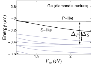
Figure 10 extends the calculations on which Fig. 4 was based, by considering a range of values of . While for , the OVS occurs, we observe that this reversed ordering of -like and -like hole levels persists only down to values . Character of the envelope functions, that allows to label the two levels as - and -like, is demonstrated in panels (c,d) of Fig. 4. In contrast to the SC and FCC lattice TB models, the degeneracy of levels in Fig. 10 is lower. Rather than two triplets seen for the SC and FCC lattice, we find a singlet and a doublet both for the -like and -like states. Both magnitude and sign (which indicates the ordering of the singlet and the doublet) of the corresponding energy splittings, , depend on the QD size and structural details. The latter is discussed in Appendix C, and here we focus on the other aspect of that decrease with increasing size of the QD. Any change in the energy offset of the - and -like levels (for example, due to the changes in ) in Fig. 10 will change the position of their crossing, . Consequently, as summarized in Table 3, the value of varies depending on the size of the QD. We find that regardless of the QD structure termination (two examples, -type and -type, referred to in Table 3 are precisely defined in Appendix C), these values tend to converge to that is lower than the bulk value of . Within our TB model of Ge, we can conclude that the OVS becomes the ground state for sufficiently large QDs made of this material. In a suitably chosen material, our findings demonstrate that -like states can be at the top of the VB. However, for more rigorous verification, there are other factors to be studied in more detail, such as next-nearest-neighbor interactions, spin-orbit interaction, and more elaborate surface passivation treatment.
In the calculations, effects arising from the atomistic QD structure that we described above, are not included. This could raise some concerns in quantitative analyses of the level positions in QDs. However, as long as the surface effects are not dominant, and TB models well agree in predicting the energy level reversal for sufficiently strong - hybridization.
| termination | 14 layers | 18 layers | 22 layers | 26 layers | |
|---|---|---|---|---|---|
| -type | 1.30 | 1.37 | 1.40 | 1.46 | |
| (eV) | -type | 3.00 | 2.56 | 2.40 | 2.30 |
IV Conclusions
In this work we provide a systematic support for the reversed level ordering of the lowest energy hole states, at the top of the VB of a semiconductor QD. In contrast to the conventional understanding, a nodal -like state can become the ground state, having a lower energy than the nodeless -like state. While some of the previous theoretical reports of such “nodal ground states” have been known in semiconductor nanostructures, there was a debate if they are just an artifact of a model applied to small QDs, outside the region of its usual validity,Bagga2006:PRB ; Li2000:PRB ; Persson2006:PRB ; Richard1996:PRB and would be absent in the first-principles calculations.DoubleQD Similar concerns could then be raised about the experimental reports of the nodal ground state and the reversed level ordering, if their interpretation excluding other possibilities also relies on the approach.Horodyska2010:PRB ; Bagga2006:PRB Furthermore, the prior reports of the nodal ground states have yet to explain their microscopic origin and the underlying mechanism for their formation.
Our results for the nodal ground states in the VB are obtained from the complementary and TB models and further supported by a simple picture from a continuum model, thus ruling out that an unconventional level ordering could be limited to an artifact of a single method. Moreover, the transparency of our approach provides also a microscopic understanding for the evolution of the nodal states to the top of the VB and the related orbital ordering. We report a striking difference between the orbital textures of the nodal and nodeless states. In particular, we explain how the nodal ground state can be associated with the orbital vortex state, whose energy is nearly independent of the - hopping parameter over a wide range of its values.
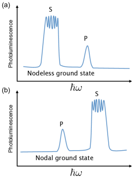
To test experimentally our predictions for the nodal ground state, we suggest considering photoluminescence measurements in QDs doped with a single magnetic impurity, typically Mn. Similar pioneering experiments have already been performed in II-VI epitaxially grown QDs.Besombes2004:PRL ; Leger2005:PRL When spin of the single Mn atom () is decoupled from from carriers in the QD, corresponding photoluminescence line will be ()-fold degenerate. The exchange interaction of the Mn and the hole spin can be expressed as,Fernandez-Rossier:2011
| (24) |
where is the hole-Mn exchange integral, and are the hole and the Mn spin operator with the Mn atom at position . This exchange interaction lifts the sixfold Mn degeneracy with the splitting proportional to the modulus squared of the wavefunction at the Mn position.
For a conventional nodeless -like hole state, the degeneracy of the observed photoluminescence would display multiple peaks in the spectrum. Experiments are often carried out with asymmetrically shaped QDs and in case of flat self-assembled QDs,Besombes2004:PRL the degeneracy of these multiplets is two, corresponding to the heavy-hole and components of the exciton. Each of the six doublets can be labelled by :Besombes2004:PRL ; Leger2005:PRL ; Fernandez-Rossier:2011 from the ground state , , to the highest energy state , . The measured magnitude of the -like state splitting in (Cd,Mn)Te QD was on the order of 1 meV.Besombes2004:PRL In contrast, if the Mn atom is located at the center of a cubic or spherical QD, the nodal -like state should suppress the hole-Mn exchange interaction (as the node in an envelope function coincides with the Mn location), producing no splitting in the photoluminescence. Schematically, these two outcomes are illustrated in Fig. 11 and could be used to identify the reversed level ordering and the nodal ground state in the VB. We also point out that from the theoretical point of view, the -like state should survive in asymmetrical QDs as we discuss in Appendix D.
In an idealized model of a strong electron and hole confinement, the optical selection rules would give a vanishing radiative transition between the orthogonal - and -like states in the CB and VB, respectively. This is not the case in realistic QDs of ill-defined parity. The photoluminescence peak for the nodal state would be partially suppressed, but not vanish, as compared to the nodeless state and indicated in Fig. 11. In fact, our proposed scenario for the photoluminescence signature of the nodal states is providing motivation to revisit measurements of QDs with single Mn.Lucien However, an appropriate identification would still require a detailed data analysis which we hope will be stimulated by our predictions for the VB orbital ordering and its implications.
Focusing on magnetically-doped QDs with many Mn impurities could also provide a useful test if our understanding of orbital ordering can lead to additional means of controlling magnetism. For example, it was predicted Abolfath2008:PRL that an electrostatic deformation of a quantum confinement could reversibly turn on and off the magnetic ordering of Mn spins, even at a fixed number of carriers. This was expected to be a consequence of the confinement-induced change in the carrier spin state. In contrast, even without changing the carrier spin state, our analysis for altering the ordering of between the nodeless and nodal states would imply a change in the exchange interaction (as indicated in Fig. 11) and thus modify the magnetic ordering.
A further motivation for our studies of nodal ground states in semiconductor nanostructures is provided by their experimental observation in other confined systems with multiband electronic structure of the host lattice near the band edge. An interesting question would be to explore related orbital textures of such nodal states. For example, a Li donor impurity in Si has an “inverted” sequence of energy levels with a nodal ground state of -like symmetry.Watkins1970:PRB ; Jagannath1981:PRB ; Pendo2013:PRB
We thank G. M. Sipahi for valuable discussions. This work was supported by the DOE-BES DE-SC0004890, NSF-DMR 0907150, and US ONR.
Appendix A: Continuum Model
Here we explain the derivation of our continuum model for square lattice in Sec. III A and the resulting effective Hamiltonian in Eq. (14). We start from - and -orbitals with on-site energies and (). -orbitals form the CB, and -orbitals form the VB. We assume that the bonding within each orbital is weak and and bandwidths are much smaller than and we can treat the - bonding (hopping) as perturbation. The unperturbed Hamiltonian in the TB model with - hopping parameter can be written as
| (A-1) |
where are dispersion relations for - and -orbitals, respectively. Here, is the Bloch state for -orbitals. The - bonding as the perturbation is given in Eq. (10). The bandwidths of are much smaller than . Then in the second order perturbation theory, through the operator for the - hybridization , the energy denominator can be replaced by .
To evaluate the second order term from Eq. (9), we note that in the square lattice with a lattice constant , we can express the effect of on atomic orbitals as
| (A-2) |
Similarly, to perform the downfolding method in Eq. (9), we can also express the effect of on -orbitals
and
Together with Eqs. (Appendix A: Continuum Model) and (Appendix A: Continuum Model), Eq. (12) is used to derive the representation of in Eq. (13) and with continuum approximation, Eq. (11) is obtained. Now, we show how the unperturbed Hamiltonian can be represented as the usual kinetic energy term. For a slowly-varying wavefunction,
| (A-5) | |||||
and
| (A-6) | |||||
If we assume that , the above result further simplifies. The effective Hamiltonian written for the two-component vector-field wavefunction can be derived from and by replacing the discrete lattice points by an integral over , we get
| (A-7) | |||||
where we have ignored the constant energy shift . Assuming that the wavefunction is zero at the boundary due to confinement potential, after integration-by-parts, we obtain Eq. (14),
| (A-8) |
where the first term is the usual -only (TB) kinetic energy, and the second term is the positive divergence contribution (in the hole representation) mediated by the CB -states. Using the above method, we can in principle derive an effective Hamiltonian for any lattice structure.
To analyze the ground state structure in the small limit, we start with the unperturbed kinetic energy eigenstates, in the two-component notation,
| (A-9) | |||||
| (A-10) |
for - and OVS (-like) states with their unperturbed energies
| (A-11) |
respectively. It is straightforward to calculate their perturbed energy in the order of ,
| (A-12) |
| (A-13) |
Using and in the limit , this result is equivalent to Eqs. (III.1) and (20). As increases, the OVS energy changes slower than that of the -like states, and the OVS eventually becomes the hole ground state.
Now, we consider the opposite limit of and . The unperturbed Hamiltonian becomes the divergence term in Eq. (LABEL:eq:A8) and its Schrödinger equation becomes
| (A-14) |
with the unperturbed energy . With the infinite potential well limit, finite and require that the vector must vanish on the boundary. Solving the differential equation with zero boundary conditions, its solutions automatically satisfy the above Schrödinger equation with . We find the ground state of the kinetic energy within the subspace of such solutions. With the observation of the ground state texture, we propose a state in a separable form, and . From the zero divergence condition, we require . The new boundary conditions on , that is and , can be accommodated by writing with . Since the proposed form of the ground state must optimize the kinetic energy, we start by a quadratic polynomial with the least curvature. The form of the polynomial can be improved variationally by including higher orders. Therefore the proposed ground state wavefunction reads,
| (A-15) |
with the normalization constant . This state preserves the -like symmetry with the zero-divergence condition strictly imposed. The agreement of this wave-function and the numerically exact solution to the continuum model, Eq. (LABEL:eq:A8), is excellent at the discrepancy of 1.1% with the error defined as for . Due to this zero-divergence condition, the unperturbed energy has no dependence and, as shown in Fig. 6(d), the energy eigenvalue of the -like state becomes independent of as . The energy of the -like state can be evaluated by the expectation value of the - kinetic energy term as,
| (A-16) |
in the limit of . It is remarkable that this expression is very close to that of the limit, Eq. (A-11), which justifies the very weak dependence throughout for all from the TB result, as shown in Fig. 6(d).
Appendix B: Tight-Binding Model for Simple Cubic, Face Centered Cubic, and Diamond Lattice
This Appendix presents more details on the various TB models discussed in the Secs. III B and C and we establish a connection between the and TB models. We first consider a bulk sample with a SC lattice having four orbitals, , , , and . The relevant parameters are the difference of the on-site energies and hopping parameters , , and as defined in Sec. III. The corresponding TB Hamiltonian is given as
| (B-5) |
where
| (B-6) |
and is the lattice constant. Using the Löwdin approximationChuang:2009 , original basis space can be folded into the reduced Hilbert space of . Then, the reduced Hamiltonian is written as,
| (B-10) |
with and , where
| (B-11) |
The effective Hamiltonian describes the VB only. Now assuming , we expand each matrix element up to the second-order in to obtain as
| (B-15) |
where , , and .
On the other hand, a Luttinger Hamiltonian can be transformed into the exactly same formLuttinger of a matrix representation as Eq. (B-15) through a basis transformation with , , and . The coefficients A, B, and C correspond to the original definition from Refs. Luttinger, ; Chow:1996, . We provide a useful correspondence between the TB hopping parameters and Kohn-Luttinger parameters,
| (B-16) | |||||
These expressions directly lead to Eq. (23).
We now proceed to describe the FCC and diamond lattice TB Hamiltonian matrices used in Secs. III B and C. The four-band FCC TB model is written as,
| (B-21) |
where,
| (B-22) | |||
| (B-23) | |||
| (B-24) | |||
| (B-25) | |||
| (B-26) | |||
| (B-27) |
Hamiltonian for the diamond lattice which contains two atoms in a primitive unit cell is written as,
| (B-28) |
where the two diagonal blocks are identical since the cation and anion atoms are the same for diamond lattice. The off-diagonal block can be expressed using parameters , , related to the parameters discussed in Sec. III C and defined by , . Following Chadi and Cohen,Chadi1975:PTSb
| (B-29) |
where
| (B-30) |
with , , and . We use Ge parameters from Ref. Chadi1975:PTSb, for the nearest-neighbors to keep our model simple and the corresponding bulk band structure is shown in Fig. 4(b).
Appendix C: Issues related to the termination and passivation of the QD structure
Compared to SC and FCC lattices, the diamond lattice allows for multiple ways
of termination in a finite-size structure. The choice of termination
as well as the properties of the surface layer of atoms (passivation)
often have a strong influence on the QD electronic structure. We start
by discussing the diamond lattice termination.
A possible procedure to construct a cubic QD
is the following. We take a stack of FCC
unit cells and combine it with its copy shifted by 1/4 of the
body diagonal. The resulting 344 atoms can be divided into 14 layers
written down as ABCDABCDABCDAB in the notation of Fig. 12(a). This
procedure corresponds to the -type termination discussed in
Sec. III C and Table 3. The other type () discussed corresponds
to DABCDABCDABCDA for 14 layers. Larger QDs are
constructed according to the same pattern: C…D (A…B) for
().
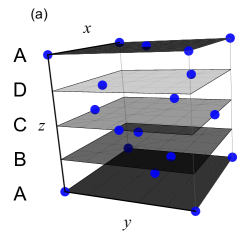
These two different lattice terminations give qualitatively different QD electronic structures in terms of the level degeneracy at the top of the VB. In the large limit, both - and -type (passivated) clusters show a -like state at the top of the VB. However, while the state is non-degenerate for -type, it forms a doublet state for the -type. This can be seen as a finite-crystal field splitting of the originally three-dimensional manifold of -like states discussed in Sec. III B for the SC and FCC lattices, a splitting that changes sign depending on the cluster termination. Regardless of this, an analogous plot to Fig. 10 showing the -dependence of energy levels in a -type cluster exhibits a crossing between - and -like levels albeit at a different (larger) value of as it is summarized in Table 3. It appears that the mechanism of the level reversal does not depend on the termination, and moreover, with a larger size of QD, the splittings, and decrease.
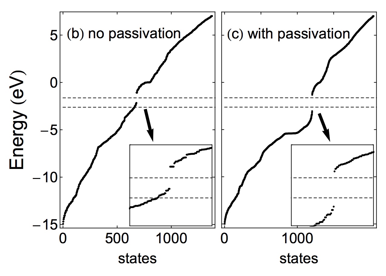
We now turn our attention to the passivation of the QD surface. If we consider the unpassivated 14-layer -type Ge QD, we find that it is difficult to identify the band gap in its spectrum. There is a gap in the sequence of energy levels as shown in Fig. 12(b) but it is shifted with respect to the bulk band gap (shown by dashed lines) and more importantly, the wavefunctions of the states at the anticipated top of the VB (and bottom of the CB) are localized at the QD surface rather than extending through the volume of the QD. Since surface passivation is known to be important both from the perspective of enhancing measured optical propertiesSalivati2009:JAP ; Yang2008:RLMS and calculated positions of energies in VB and CB,Hapala2013:PRB ; Yu2006:APL we have added an extra atomic layer to the clusters which we investigated, making sure that there remains no dangling bond of the QD core. The passivation layer atoms are assumed to have the same hopping to the QD core atoms as the core atoms between each other and to keep the model simple, we assign a single on-site energy to their - and -orbitals. In our convention, is taken relative to the on-site energy of QD core atom -orbitals. By adjusting sufficiently far from the bulk band gap region, we remove the states localized at the surface from the gap and recover the band gap in the QD spectrum as it can be seen in Fig. 12(c). For all calculations with passivated Ge QDs in this article, we use eV.
Appendix D: Geometrical Factor in Energy Ordering
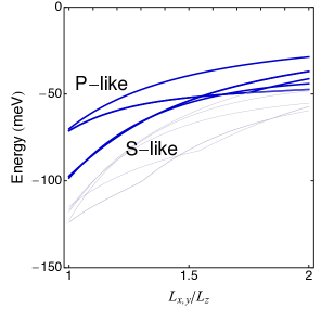
The geometry of actual QDs investigated in experiments deviates from a perfectly spheric or cubic shape. Our analysis has so far focused on a simple cubic geometry. Although the termination and passivation issues discussed in Appendix C already reduce the level of perfection of the QD shape, it is useful to estimate how geometrical changes in QD influence energy level ordering.
Using the same approach as in Ref. 61, we calculate levels in a nm InAs QD of cuboid shape . Material parameters for this calculation were taken from Table I (without spherical approximation) but was set to zero. As Fig. 13 shows, the originally threefold degenerate -like and -like levels split as the aspect ratio deviates from one. The top level of the VB is a -like doublet and even though its separation in energy from the lower-lying -like state decreases with increasing , the two levels do not cross up to aspect ratios as large as five. These results support the view of the -like ground state as a robust feature of QDs fabricated from a suitably chosen material.
Appendix E: Perturbative Analysis of the Tight-Binding Models
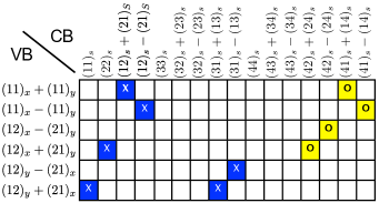
We have already given an example of the coupling rules for of Eq. (9) between the VB and CB states in Eq. (17). For a general CB state and a general VB state or , the matrix elements of defined in Eq. (10) can be written down analytically. They take on a particularly simple form in the continuum () limit,
| (E-1) |
where if and are both odd or both even and otherwise.
We focus on the two -like states given in Eq. (15) and four -like states given in Eq. (16) that are degenerate when . After a transformation applied to to the -like states, the six VB states of our interest can be listed as shown in the left column of Fig. 14. CB states can also be represented in an analogous manner in order to make our analysis clear. It turns out that most matrix elements of between these six VB states and CB states vanish. In Fig. 14, large (small) non-zero matrix elements for the given pair of VB and CB states are indicated by a cross (circle). If we choose a VB state, we can determine how strongly its energy depends on by inspection of the corresponding row in the table. To the second order of the perturbative analysis, the energy correction is proportional to multiplied by the sum of squared matrix elements. We can convince ourselves that in five of the six rows of Fig. 14, there is always at least one large matrix element. The row which contains only small matrix elements corresponds to the state which is the OVS of Eq. (18). The consequent weak -dependence of this state’s energy is at the root of the level crossing in Fig. 6(d).
The weak interaction of OVS with the CB levels is due to OVS symmetry which renders the couplings to the low- CB states zero. The lowest CB state to which OVS couples is and because of the large and involved in this state, the coupling matrix element in Eq. (E-1) is relatively small compared to the couplings in other rows of Fig. 14.
References
- (1) M. P. Marder, Condensed Matter Physics, 2nd Edition (Wiley, New York, 2010).
- (2) D. W. Snoke, Solid State Physics: Essential Concepts (Addison-Wesley, New York, 2008).
- (3) O. Gywat, H. J. Krenner, and J. Berezovsky Spins in Optically Active Quantum Dots, (Wiley, New York, 2010).
- (4) M. P. Persson and H. Q. Xu, Phys. Rev. B 73, 125346 (2006).
- (5) A. Bagga, P. K. Chattopadhyay, and S. Ghosh, Phys. Rev. B 68, 155331 (2003).
- (6) A. Bagga, P. K. Chattopadhyay, and S. Ghosh, Phys. Rev. B 71, 115327 (2005).
- (7) A. Bagga, P. K. Chattopadhyay, and S. Ghosh, Phys. Rev. B 74, 035341 (2006).
- (8) Z. Yu, J. Li, D. B. O’Connor, L.-W. Wang, and P. F. Barbara, J. Phys. Chem. B 107, 5670 (2003).
- (9) M. Nirmal, D. J. Norris, M. Kuno, M. G. Bawendi, Al. L. Efros, and M. Rosen, Phys. Rev. Lett. 75, 3728 (1995).
- (10) Al. L. Efros, M. Rosen, M. Kuno, M. Nirmal, D. J. Norris, and M. Bawendi, Phys. Rev. B 54, 4843 (1996).
- (11) J. Seufert, G. Bacher, M. Scheibner, A. Forchel, S. Lee, M. Dobrowolska, and J. K. Furdyna, Phys. Rev. Lett. 88, 027402 (2001).
- (12) R. Beaulac, L. Schneider, P. I. Archer, G. Bacher, and D. R. Gamelin, Science 325, 973 (2009).
- (13) F. Xiu, Y. Wang, J. Kim, P. Upadhyaya, Yi Zhou, X. Kou, W. Han, R. K. Kawakami, J. Zou, and K. L. Wang., ACS Nano 4, 4948 (2010).
- (14) D. A. Bussian, S. A. Crooker, M. Yin, M. Brynda, A. L. Efros, and V. I. Klimov, Nature Mater. 8, 35 (2009).
- (15) I. R. Sellers, R. Oszwałdowski, V. R. Whiteside, M. Eginligil, A. Petrou, I. Žutić, W.-C. Chou, W. C. Fan, A. G. Petukhov, S. J. Kim, A. N. Cartwright, and B. D. McCombe, Phys. Rev. B 82, 195320 (2010).
- (16) J. Fernández-Rossier and L. Brey, Phys. Rev. Lett. 93, 117201 (2004).
- (17) W. Zhang, T. Dong, and A. O. Govorov, Phys. Rev. B 76, 075319 (2007).
- (18) A. O. Govorov, Phys. Rev. B. 72, 075359 (2005).
- (19) R. M. Abolfath, A. G Petukhov and I. Žutić, Phys. Rev. Lett. 101, 207202 (2008).
- (20) Y. Léger, L. Besombes, L. Maingault, D. Ferrand, and H. Mariette, Phys. Rev. Lett. 95, 047403 (2005).
- (21) J. Fernández-Rossier and R. Aguado, in Handbook of Spin Transport and Magnetism, edited by E. Y. Tsymbal and I. Žutić (CRC Press, New York, 2011).
- (22) R. Oszwałdowski, I. Žutić, and A. G. Petukhov, Phys. Rev. Lett. 106, 177201 (2011).
- (23) J. M. Pientka, R. Oszwaldowski, A. G. Petukhov, J. E. Han and I. Žutić, Phys. Rev. B 86, 161403(R) (2012).
- (24) L. Besombes, Y. Léger, L. Maingault, D. Ferrand, H. Mariette, and J. Cibert, Phys. Rev. Lett. 93, 207403 (2004).
- (25) F. Henneberger and J. Puls, in Introduction to the Physics of Diluted Magnetic Semiconductors edited by J. Kossut and J. A. Gaj (Springer, Berlin, 2010).
- (26) H. Fu, L. W. Wang, and A. Zunger, Appl. Phys. Lett. 71, 3433 (1997)
- (27) L. W. Wang and A. Zunger, J. Phys. Chem. B 102, 6449 (1998)
- (28) L. W. Wang, A. J. Williamson, A. Zunger, H. Jiang, and J. Singh, Appl. Phys. Lett. 76, 339 (2000).
- (29) P. M. Morse and H. Feshbach, Methods of Theoretical Physics, Vol. 1 (McGraw-Hill, New York, 1953).
- (30) P. Yu and M. Cardona, Fundamentals of Semiconductors, 2nd ed. (Springer, New York, 2010).
- (31) R. Winkler, Spin-orbit Coupling Effects in Two-Dimensional Electron and Hole Systems, (Springer, New York, 2003).
- (32) F. Meier and B. P. Zakharchenya, Eds. Optical Orientation (North-Holland, New York, 1984).
- (33) M. I. Dyakonov, Ed., Spin Physics in Semiconductors (Springer, Berlin, 2008).
- (34) H.-J. Drouhin, C. Hermann, and G. Lampel, Phys. Rev. B 31, 3859 (1985)
- (35) S. Murakami, N. Nagaosa, and S.-C. Zhang, Science 301, 1348 (2003).
- (36) M. Z. Hasan and C. L. Kane, Rev. Mod. Phys. 82, 3045 (2010).
- (37) E. Bernardes, J. Schliemann, M. Lee, J. C. Egues, and D. Loss, Phys. Rev. Lett. 99, 076603 (2007)
- (38) G. Bastard, Wave Mechanics Applied to Semiconductor Heterostructures, (Wiley, New York, 1991); M. Willatzen and L. C. L. Y. Voon, The kp method, (Springer, New York, 2009)
- (39) J. M. Luttinger, and W. Kohn, Phys. Rev. 97, 869 (1955); J. M. Luttinger, Phys. Rev. 102, 1030 (1956).
- (40) A. Baldereschi and N. O. Lipari, Phys. Rev. B 8, 2697 (1973).
- (41) Our basis in which we write down the matrix of the Hamiltonian in Eq. (2) comprises direct products of the eigenstates and envelope functions . The unperturbed -like wavefunction corresponds to . Throughout the paper , except for Fig. 3(b) with well-in-well structure, where a smaller QD () structure is confined by finite potential in a larger infinite potential well () with .
- (42) K. Výborný, J. E. Han, R. Oszwałdowski, I. Žutić, and A. G. Petukhov, Phys. Rev. B 85, 155312 (2012).
- (43) M. Abolfath, T. Jungwirth, J. Brum, and A. H. MacDonald, Phys. Rev. B 63, 054418 (2001).
- (44) Fig. 2 of Ref. Vyborny2012:PRB, also shows that for suitable values of , -like state may be energetically favorable to the common nodeless ground st3ate (-like state). Note that numerical results of Ref. Vyborny2012:PRB, are slightly different from the results obtained using six-band model in the limit due to an erroneous sign in some matrix elements of Eq. (2) in Ref. Vyborny2012:PRB, .
- (45) nm is chosen in order to verify our calculation with the experimental and theoretical bandstructure of a GaAs Quatum Well; J. A. Kash, M. Zachau, M. A. Tischler, and U. Ekenberg, Phys. Rev. Lett. 69 2260 (1992)
- (46) J. C. Slater and C. F. Koster, Phys. Rev. 94, 1498 (1954).
- (47) W. A. Harrison, Electronic Structure and the Properties of Solids, (Dover, New York, 1989).
- (48) Note that the -like manifold is precisely only at . At finite , the two wavefunctions acquire admixtures from other states defined by Eq. (8) but they remain degenerate. This degeneracy is due to the -rotation symmetry.
- (49) W. Jaskólski, R Oszwałdowski, and G. W. Bryant, Vacuum 63, 191 (2001).
- (50) P. Hapala, K. Kůsová, I. Pelant, and P. Jelínek, Phys. Rev. B 87, 195420 (2013).
- (51) D. J. Chadi and M. L. Cohen, Phys. Stat. Sol. (b) 68, 405 (1975).
- (52) J. Li and J. B. Xia, Phys. Rev. B 61, 15880 (2000).
- (53) T. Richard, P. Lefebvre, H. Mathieu, and J. Allègre, Phys. Rev. B 53, 7287 (1996).
- (54) The situation can be different in a double QD where the first-principles calculation would also suggest a possibility for a nodal ground state as in G. Bester, A. Zunger, and J. Shumway, Phys. Rev. B 71, 075325 (2005). This possibility was supported by both a model and experiments in M. F. Doty, J. I. Climente, M. Korkusinski, M. Scheibner, A. S. Bracker, P. Hawrylak, and D. Gammon, Phys. Rev. Lett. 102, 047401 (2009).
- (55) P. Horodyská, P. Němec, D. Sprinzl, P. Malý, V. N. Gladilin, and J. T. Devreese, Phys. Rev. B 81, 045301 (2010).
- (56) L. Besombes, private communication.
- (57) G. D. Watkins and F. S. Ham, Phys. Rev. B 1, 4071 (1970).
- (58) C. Jagannath and A. K. Ramdas, Phys. Rev. B 23, 4426 (1981).
- (59) L. Pendo, E. M. Handberg, V. N. Smelyanskiy, and A. G. Petukhov, Phys. Rev. B 88, 045307 (2013).
- (60) S. L. Chuang, Physics of Photonic Devices, 2nd ed. (Wiley, New York, 2009)
- (61) W. W. Chow, S. W. Koch, M. Sargent, Semiconductor-Laser Physics, (Springer, New York, 2010).
- (62) N. Salivati, N. Shuall, E. Baskin, V. Garber, J. M. McCrate, and J. G. Ekerdt, J. Appl. Phys. 106, 063121 (2009).
- (63) P. Yang and M. Bredol, Res. Lett. in Mater. Sci. 2008, Article ID 506065 (2008).
- (64) M. Yu, G. W. Fernando, R. Li , F. Papadimitrakopoulos, N. Shi, and R. Ramprasad, Appl. Phys. Lett. 88, 231910 (2006).