Gate controlled spin pumping at a quantum spin Hall edge
Abstract
We propose a four-terminal device designed to manipulate by all electrical means the spin of a magnetic adatom positioned at the edge of a quantum spin Hall insulator. We show that an electrical gate, able to tune the interface resistance between a quantum spin Hall insulator and the source and drain electrodes, can switch the device between two regimes: one where the system exhibits spin pumping and the other where the adatom remains in its ground state. This demonstrates an all-electrical route to control single spins by exploiting helical edge states of topological materials.
In recent years topological insulators and their two-dimensional analogs, quantum spin Hall (QSH) insulators, have been intensively investigated review-kane ; review-zhang . Much of the excitement is due to their time-reversal symmetry protected edge states, which are immune to non-magnetic disorder. At a given edge spins of opposite direction counterpropagate, giving rise to spin-momentum locked helical states. These carry dissipationless current and appear promising for future spintronic applications spin-pesin . Already a number of proposals for devices utilizing these spin-momentum locked states have appeared. These range from topological spin transistors qi-spinaharonov to magnetoresistive devices burkov-magnetores , just to name a few. In parallel with these developments, rapid strides have been made in the precise control and manipulation of single atomic spins on insulating substrates by means of a Scanning Tunneling Microscope (STM) tip Heinrich2004 ; Loth1 . Indeed it is now possible to measure the conductance spectra of these single atomic spins on nonmagnetic substrates at a rather low temperature and in high magnetic fields. Advances in low-temperature STM have also allowed the detection of inelastic spin excitations in such setups and this has been termed spin-flip inelastic electron tunneling spectroscopy (sf-IETS).
Inspired by the rapid developments in the two fields, we have showed in a recent study that the spin of a magnetic adatom could be manipulated by using the helical edge states of a QSH insulator sanvito-IETS . We found that, depending on the current intensity, electron transport presents two regimes: i) for a small current density there is suppression of the inelastic component of the conductance spectrum and, in contrast, ii) when the current density is large the conductance steps characteristic of the inelastic transitions re-appear. In the second regime spin angular momentum is pumped into the magnetic adatom, so that single spin manipulation by electrical means, a spintronics holy grail, is achieved. Here we extend the concept and propose a device where the transition between the two regimes is also achieved electrically, by gating the region at the boundary between the QSH insulator and the source/drain electrodes. As such we will show that the QSH state can be coupled with sf-IETS to probe and manipulate single magnetic atoms without the need of a magnetic field or a spin-polarized STM tip.
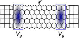
The device setup is shown schematically in Fig. 1. It consists of two electrodes, described by a simple square lattice, sandwiching a QSH ribbon, which acts as scattering region. The magnetic adatom is positioned at one of the edges of the ribbon. Furthermore, we include two gate potentials at both the left-hand and right-hand side ends of the ribbon. The QSH ribbon is modeled by means of Kane-Mele Hamiltonian constructed on a honeycomb lattice kane-mele ,
| (1) | ||||
The first term is a staggered sublattice potential of strength ( for two sublattices of the honeycomb lattice). The second term is the nearest neighbor hopping with strength (we now set ). Finally the third term, which is crucial for the topological phase, is a complex next nearest neighbor hopping with strength . This spin-orbit-mimicking term couples electrons’ orbital motion to their spins via the -component of the Pauli matrices (), with having opposite sign for opposite directions of hopping. Although the spin-orbit term is too weak in graphene to observe this effect at realistic temperatures, recent proposals for silicene and its germanium analog have reported spin-orbit-driven bandgaps of 2.9 meV and 23.9 meV, respectively silicene-yao . Furthermore, Xu et al. have predicted two-dimensional Sn films to have spin-orbit gaps of 300 meV, which is comparable to that of the three-dimensional topological insulators currently known sn-zhang . These materials exhibit a low energy physics, which is well described by the Kane-Mele model.
In the presence of the gate voltages and of an adatom at site , the total electronic Hamiltonian becomes
| (2) |
where in addition to , we have the gate potential , which is included via an additional on-site energy for the atoms in the gate region at the two ends of the ribbon. We have also included the on-site potential of the magnetic impurity, , and the hopping between the impurity site and its neighbor on the honeycomb lattice. For the magnetic impurity spin we further introduce the Hamiltonian
| (3) |
where describes a uniaxial anisotropy (along , which is the direction normal to the plane of the QSH ribbon) with strength . The coupling of the conduction electrons and the impurity spin is through the term , with magnitude . This Heisenberg-type coupling is the so-called - model sdmodel .
The many-body problem introduced above is solved by perturbation theory in . Here we outline only briefly the perturbation expansion needed to calculate the interacting self-energy and the spin state of the adatom, and we refer the readers to Refs. Hurley1 ; Hurley3 for more mathematical details. The single-particle Green’s function in the many-body ground state can be expanded to the -th order in the interaction Hamiltonian. In this work we have truncated the expansion in the electron and spin propagator to the second-order. Then, we use Dyson’s equation to calculate the interacting self-energy, which are then converted to real-time quantities by using Langreth’s theorem. The dependence of the self-energy on the energy is then obtained by Fourier transform. The population of the spin states is evaluated from a master equation sanvito-IETS , which derives from the equation of motion for the spin propagator. Finally the net magnetization of the impurity spin is obtained by averaging over the population of all states.
In order to calculate the current we use the Landauer-Büttiker approach Buttiker implemented in terms of the non-equilibrium Green’s function (NEGF) method Datta and the conductance is then extracted as a numerical derivative. The retarded Green’s function for the scattering region is given by, , where ( L, R) are the self-energies of the left-hand and right-hand side leads. The electron-spin coupling is taken into account via the interacting self-energy . Finally, the current can be calculated as
| (4) |
where () are the lesser and greater self-energies (Green’s functions).
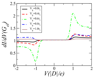
We begin our analysis by looking at the conductance spectra (normalized to its value, ) at different values of the gate voltage, . The results are presented in Fig. 2. For the calculations we set and ( is the hopping parameter in the electrodes and is the coupling between the electrodes and the scattering region). These parameters keep the ribbon in the topological phase and the coupling between the leads and the scattering region is fixed to a large value. The choice of parameters, and , guarantees that perturbation theory can be used for the spin . The spin degeneracy is lifted by introducing an axial anisotropy . This is equivalent to a temperature of around 12 K (assuming a realistic value of ). In general, devices based on single atom anisotropies are low temperature devices expected to work around few tens of kelvin Heinrich2004 ; Loth1 .
At , i.e. when no gate voltage is applied, there is a conductance step seen at the energy corresponding to the first spin excitation of the system. This is the () spin transition for positive (negative) source/drain voltage, where is the adatom spin third component sanvito-IETS . Such transition is detectable because the electrode-ribbon coupling strength is large and the current is intense. As we increase the gate voltage we observe an enhancement in the intensity of the conductance step. This continues utill reaches a value of . Beyond such critical gate voltage there is a drop in the conductance step at and the inelastic conductance becomes suppressed. This suppression continues for higher values of the gate voltage.
These observations can be readily understood in terms of the changing the interface resistance between the ribbon and the electrodes. At low values of , there is a large current flowing from the leads to the ribbon and thus interacting with the magnetic adatom. For the spin on the adatom is in an equal superposition of and states. As the bias reaches the excitation to the state is possible by spin-flip of the incoming electron. Since the current is large the impurity spin is not allowed to relax back to the ground state and thus the incident electrons can also induce transitions from to and so be transmitted without getting backscattered.
In the case of high interface resistance as engineered by increasing the gate voltage, there is a strong suppression of the conductance steps. In this scenario since the current density is small, the impurity spin can relax back to the ground state after the spin-flip event. This means that the incident right-going electrons, which are up spin polarized at the upper edge, will always encounter the impurity spin in either the or the state. A spin-flip event will reverse the electron’s spin and since there are no down spin channels going right at the upper edge, the electron will be backscattered. Thus, the helicity of the QSH edge states leads to a suppression of the inelastic conductance steps at low currents sanvito-Andreev .
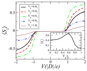
Finally in Fig. 3 we plot the average magnetization of the device at different gate voltages. If no gate voltage is applied then a change from zero to a finite magnetization occurs at , corresponding to the allowed spin excitation. Note that the direction of magnetization is opposite for opposite bias directions. As we now increase the gate voltage, the net magnetization increases, tending towards unity. This continues until beyond which it drops rapidly. For higher values of the system remains closer to zero magnetization indicating the absence of spin pumping. The inset of Fig. 3 traces the magnetization at as a function of the gate voltage. Note that the magnetization is always less than , due to finite size of the QSH ribbon.
In conclusion, we have studied the spin pumping of a quantum spin at a topological insulator edge. In particular we have proposed a device concept in which an electrostatic gate in a two-terminal device allows the device switching between two regime. In the first inelastic conductance steps are suppressed, while in the second they are allowed. This second regime offers the possibility of manipulating impurity spins using the helical edge states of a QSH insulator. Thus, we have proposed a complete all-electrical device which allows control of a quantum spin without using any magnetic field.
This work is supported by Irish Research Council (AN) and Science Foundation of Ireland (AH, grant No. 07/IN.1/I945). Computational resources have been provided by Trinity Center for High Performance Computing. We acknowledge illuminating discussions with Cyrus Hirjibehedin, Ivan Rungger and Nadjib Baadji.
References
- (1) M.Z. Hasan and C.L. Kane, Rev. Mod. Phys. 82, 3045 (2010).
- (2) X.-L. Qi and S.-C. Zhang, Rev. Mod. Phys. 83, 1057 (2011).
- (3) D. Pesin and A.H. MacDonald, Nat. Mater. 11, 409 (2012).
- (4) J. Maciejko, E.-A. Kim, and X.-L. Qi, Phys. Rev. B 82, 195409 (2010).
- (5) A.A. Burkov and D.G. Hawthorn, Phys. Rev. Lett. 105, 066802 (2010).
- (6) A.J. Heinrich, J.A. Gupta, C.P. Lutz, and D.M. Eigler, Science 306, 466 (2004).
- (7) S. Loth, C.P. Lutz, and A.J. Heinrich, Nature Physics 6, 340 (2010).
- (8) A. Hurley, A. Narayan, and S. Sanvito, Phys. Rev. B 87, 245410 (2013).
- (9) C.L. Kane and E.J. Mele, Phys. Rev. Lett 95, 226801 (2005).
- (10) C.-C. Liu, W. Feng and Y. Yao, Phys. Rev. Lett. 107, 076802 (2011).
- (11) Y. Xu, B. Yan, H.-J. Zhang, J. Wang, G. Xu, P. Tang, W. Duan and S.-C. Zhang, arXiv:1306.3008.
- (12) A. Hurley, N. Baadji, and S. Sanvito, Phys. Rev. B 84, 035427 (2011).
- (13) A. Hurley, N. Baadji, and S. Sanvito, Phys. Rev. B 86, 125411 (2012).
- (14) K. Yosida, Theory of Magnetism (Springer-Verlag, Berlin, 1998)
- (15) M. Buttiker, Phys. Rev. B 38, 9375 (1988).
- (16) S. Datta, Electronic Transport in Mesoscopic Systems (Cambridge University Press, Cambridge, 1997)
- (17) A. Narayan and S. Sanvito, Phys. Rev. B 86, 041104(R) (2012).