Spin transistor operation driven by the Rashba spin-orbit coupling in the gated nanowire
Abstract
The theoretical description has been proposed for the operation of the spin transistor in the gate-controlled InAs nanowire. The calculated current-voltage characteristics show that the current flowing from the source (spin injector) to the drain (spin detector) oscillates as a function of the gate voltage, which results from the precession of the electron spin caused by the Rashba spin-orbit interaction in the vicinity of the gate. We have studied two operation modes of the spin transistor: (A) the ideal operation mode with the full spin polarization of electrons in the contacts, the zero temperature, and the single conduction channel corresponding to the lowest-energy subband of the transverse motion and (B) the more realistic operation mode with the partial spin polarization of the electrons in the contacts, the room temperature, and the conduction via many transverse subbands taken into account. For mode (A) the spin-polarized current can be switched on/off by the suitable tuning of the gate voltage, for mode (B) the current also exhibits the pronounced oscillations but with no-zero minimal values. The computational results obtained for mode (B) have been compared with the recent experimental data and a good agreement has been found.
I Introduction
The all-electrical control of the spin-polarized current is a basic principle of the operation of novel spintronic devices including the spin transistor proposed by Datta and Das.Datta and Das (1990) According to this idea Datta and Das (1990) the current of spin polarized electrons injected from the ferromagnetic source contact into a semiconductor is modulated by the Rashba spin-orbit interaction (SOI)Bychkov and Rashba (1984) in a conduction channel. The state of the spin transistor depends on the spin orientation of the electron in the conduction channel with respect to the magnetization of the ferromagnetic drain contact. The successful operation of the spin transistor requires an efficient spin injection from the ferromagnetic sourceMatsuyama et al. (2002) into the semiconductor and an effective method of manipulation of the electron spin in the conduction channel. The efficiency of the spin-polarized current injection from the ferromagnetic electrode into the semiconductor is rather low.Schmidt et al. (2000) In order to improve this efficiency the semiconductor spin filter based on the dilute magnetic semiconductor heterostructure has been applied.Slobodsky et al. (2003) The operation of the paramagnetic resonant tunneling diode (RTD) as the spin filter at low temperature was demonstrated experimentally by Slobodskyy et al.Slobodsky et al. (2003) and investigated theoretically in our previous paper.Wójcik et al. (2012) However, the operation of the paramagnetic RTD as the spin filter requires a low temperature and a high magnetic field.Slobodsky et al. (2003); Wójcik et al. (2012) The fabrication of the spin filter from the ferromagnetic semiconductor allows to extend the applicability of the spin filter operation to the room temperature without the external magnetic field. In our recent paper,Wójcik et al. (2013) we have studied the spin filter effect in the mesa-type RTD based on ferromagnetic GaMnN and shown that – in this device – the spin filter operation can be realized at the room temperature.
The effective manipulation of the electron spin in a semiconductor can be realized by the Rashba SOI that couples the linear momentum of the electron with its spin via the external electric field. In the last years, the application of the SOI to the manipulation of electron spins in semiconductor nanodevices has been a subject of numerous papers.Schliemann et al. (2003); Flindt et al. (2006); Liu et al. (2006); Fasth et al. (2007); Liu et al. (2007); Ohno and Yoh (2007, 2008); Nazmitdinov et al. (2009); Gelabert and Serra (2011); Bringer and Schäpers (2011); Thorgilsson et al. (2012); Yoh et al. (2012); Ban and Ya (2013); Sadreev and Sherman (2013) In Ref. Gelabert and Serra, 2011, the conductance oscillations due to the Rashba SOI have been investigated in two-dimensional stripes. The electron spin modification in semiconductor nanowires has been studied in Refs.Bringer and Schäpers (2011); Ban and Ya (2013); Sadreev and Sherman (2013) Bringer and SchäpersBringer and Schäpers (2011) demonstrated the spin precession and modulation in a cylindrical nanowire resulting from the Rashba SOI. The shape-dependent spin transport has been studied in semiconductor nanowires without and with the SOI taken into account.Ban and Ya (2013) Moreover, the joint effect of the ac gate voltage, constant magnetic field, and the Rashba SOI on the electron transmission in the nanowire has been considered in Ref.Sadreev and Sherman, 2013. These studies have led to a realization of the spin transistor in the semiconductor layer heterostructuresWunderlich et al. (2010); Betthausen et al. (2012) and nanowires.Yoh et al. (2012) Recently, Yoh et al.Yoh et al. (2012) have fabricated the spin transistor based on the InAs nanowire and reported the gate-voltage controlled on/off switching of the current.
In this paper, we present the computational results for the spin transistor operation in InAs nanowire with the side gate electrode. These results allow us to extract the most important physical properties that underly the operation of the nanowire spin transistor. We show that the gate-voltage induced SOI in the nanowire leads to the current oscillations as a function of the gate voltage. We have studied the spin transistor operation under the ideal conditions, i.e., the full spin polarization of the electrons in the contacts at zero temperature using the one-subband approximation, and the more realistic conditions with the partial spin electron polarization in the contacts at a room temperature in the many-subband approximation. The results obtained for the second case have been compared with the experimental data. The paper is organized as follows: in Section II, we present the theoretical model, the results are presented in Section III, Section IV contains the conclusions and summary.
II Theory
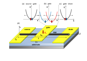
We consider the InAs nanowire with the nearby gate that generates the transverse homogeneous electric field of finite range (Fig. 1). The one-electron Hamiltonian has the form
| (1) |
where is the effective mass of the conduction band electron and . The potential energy of the electron
| (2) |
is the sum of the lateral (transverse) confinement potential energy , potential energy in the (longitudinal) electric field , where is the drain-source voltage, is the elementary charge (), and is the length of the nanowire, and potential energy in the (transverse) electric field generated by the gate, where function determines the potential energy profile along the nanowire axis. In the present paper, we take on
| (3) |
For sufficiently large () in the central region of the nanowire, i.e., near the gate of width [cf. Fig. 1(d)], and otherwise. The last term in Eq. (1) describes the Rashba SOI and has the form
| (4) |
where is the Rashba coupling constant, is the Pauli matrix vector, and .
We assume that the lateral confinement potential is strong and has the hard-wall shape.
This means that is flat inside the nanowire, i.e., in Eq. (4), the first derivative
of disappears inside the nanowire,
while the wave function of the transverse size-quantized
motion vanishes at the surface of the nanowire. Therefore,
we neglect the contribution of lateral confinement to the Rashba Hamiltonian (4). Moreover,
the contribution stemming from the longitudinal drain-source electric field
is also negligible, since this field is a few orders of magnitude smaller
than the electric field generated by the gate.
Under these assumptions Hamiltonian (4) takes on the form
| (5) | |||||
We calculate the expectation value of in the transverse state and obtain
| (6) |
where the last term results from the position-dependent SOI and assures the hermiticity of the Hamiltonian. Finally, the effective one-dimensional Hamiltonian takes on the form
| (7) | |||||
where is the energy of the -th transverse state and is the average distance between the gate electrode and nanowire
We have calculated the spin-dependent reflection and transmission coefficients for subband using the transfer matrix method on the grid with mesh points , where and has been taken to be . According to the transfer matrix method, we assume that the wave function and the current density are continuous at the interfaces between subintervals and . The continuity condition for the wave function corresponding to the transverse state has the form
| (8) |
where is the -subband wave function in the subinterval . The continuity of the current density is equivalent to the following condition:
| (9) |
where is the velocity operator, which in the presence of the SOI has the form
| (10) |
When applying conditions (8) and (9) we assume that the SOI is constant in each subinterval , which is compatible with the basic assumption of the transfer matrix method. In each subinterval , the wave function has the spinor form
| (15) | |||
| (20) |
where the component of the wave vector is given by
| (21) |
with
| (22) |
where is the energy of the electron, , and .
The dispersion relations for the different regions of the nanowire
are depicted in Fig. 1(a-c).
The quantum states of the electrons with opposite spins are degenerate in
the source-gate and gate-drain regions. This degeneracy is lifted
near the gate due to the gate-induced spin-orbit interaction.
The spin up () and spin down () amplitudes are given by
| (23) | |||||
| (24) |
For each subband we calculate the probabilities of the following processes:
the reflection with the spin conservation, i.e., no-spin-flip reflection ( and ),
the reflection with the spin flip ( and ),
the transmission with the spin conservation, i.e., no-spin-flip transmission ( and ,
and the transmission with the spin flip ( and ).
Here and in the following part of the paper, we are using subscripts ()
for the spin up (down) states.
In these calculations, we have neglected the intersubband transitions.
Having determined the transmission coefficients we have calculated the current in the ballistic regime using the Landauer formula
| (25) |
where and corresponds to the spin of the electron in the source and drain, respectively, and is the maximum number of the transverse subbands taken into account. In Eq. (25), is the Fermi-Dirac distribution function for the electrons in the source () with chemical potential and drain () with chemical potential . In order to describe the polarizing effect of the contacts we introduce polarization defined as follows:
| (26) |
where is the concentration of electrons with spin at the Fermi level. In the present paper, we neglect the resistance at the ferromagnet/semiconductor interface, which means that the electrons with the well-defined spin are injected from the ferromagnetic source into the nanowire with the 100% efficiency. Therefore, the spin current components are calculated as follows:
| (27) |
and
| (28) |
The total current is given by
| (29) |
The present calculations have been performed for the InAs nanowire with the following material parameters: , where is the free electron mass, nm2, and . In order to fulfil the conditions of the ballistic transport, we have chosen the geometric parameters of the nanowire as follows: nm and nm. The transverse states have been calculated under assumption that the nanowire possesses the square-shape cross-section with side width nm. Moreover, the infinite hard-wall potential in the transverse direction has been assumed. Since the gate can be treated as the plane capacitor with interelectrode distance nm,Yoh et al. (2012) we convert electric field of the gate to gate voltage as follows: , which allows us to present the results as functions of the gate voltage.
III Results
In this section, we present the results for the two operation modes of the spin transistor. In Subsection A, we present the results for the ideal operation mode, i.e., for the full spin polarization () of the electrons at the Fermi level in the source and drain contacts. We assume the zero temperature and the single-channel electron transport, i.e., the conduction via the lowest-energy subband of the transverse motion. In Subsection B, we present the computational results for the more realistic operation mode, i.e., for the partial polarization () of electron spins in the contacts and compare them with the experimental data.Yoh et al. (2012) These calculations have been performed at the room temperature in the framework of the many subband approximation.
III.1 Ideal operation mode
The one-subband approximation takes into account only the lowest-energy subband of the transverse size-quantized motion. This approximation can be justified for the strong lateral confinement that occurs in very thin nanowires, in which the electron occupies the lowest-energy transverse quantum state. In these calculations, we assume that only the electrons with spin up are injected from the source into the nanowire and can be detected in the drain. Moreover, we take on (for simplicity we omit index ) and choose meV.
In Fig. 2 we present the transmission coefficients for the no-spin-flip [Fig. 2(a)] and spin-flip [Fig. 2(b)] transitions.
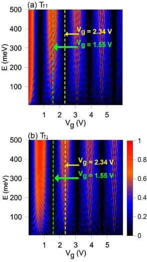
Fig. 2 shows that the transmission coefficients and are oscillating functions of the gate voltage with the period of the oscillations V. The spin-flip and no-spin-flip transmission coefficients oscillate in anti-phase. We have chosen the values of the gate voltage that correspond to the maximum ( V) and minimum ( V) of the transmission coefficient (cf. vertical dashed lines in Fig. 2). The corresponding transmission and reflection coefficients as a function of the incident electron energy are depicted in Fig. 3, which shows that the transmission and reflection coefficients are oscillating functions of the incident electron energy.
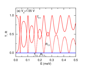
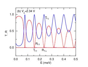
The amplitude of these oscillations decreases with the increasing energy. For V the no-spin-flip transmission and reflection coefficients oscillate taking on the values between 0 and 1, while the corresponding spin-flip coefficients ( and ) are equal to zero [Fig. 3(a)]. The opposite behaviour is observed in Fig. 3(b), in which the spin-flip transport dominates and the spin-conserved transport vanishes.
The oscillations of the transmission presented in Fig. 2 lead to the similar oscillations of the spin-polarized currents as functions of the gate voltage. Figure 4 displays spin-polarized current components and as functions of the drain-source voltage and the gate voltage. We see that spin-flip and no-spin-flip currents oscillate in anti-phase with the minimal values equal zero. The current-voltage characteristics calculated for the chosen values of gate voltage are plotted in Fig. 5(a). We note that only the spin-up electrons can pass through the drain, i.e., total current , which results from Eqs. (27), (28), and (29) for . The curve of drawn for V corresponds to the on-state of the spin transistor and exhibits the typical features for the transistor operation: for the low drain-source voltage the current rapidly increases and becomes saturated for the higher drain-source voltage. The small oscillations of the current for V result from the transmission via the higher-energy resonance states formed in the quantum-well region near the gate. For V, , which means that the spin transistor is in the off-state.
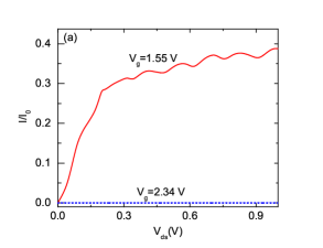
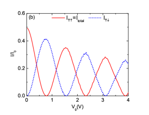
Figure 5(b) shows that total current
is the oscillating function of the gate voltage.
The spin-flip current oscillates in anti-phase and – due to the polarizing effect of the drain –
can not flow in the circuit.
The results of Fig. 5(b) demonstrate that the spin-polarized current can be switched on/off
by the suitable tuning of the gate voltage.
In order to get a more physical insight into the electron spin dynamics in the nanowire we have calculated the spin density, which is defined as follows:
| (30) |
where () and is the Hermitian conjugate of spinor . The results presented in Fig. 6 [insets (a) and (b)] show that the spin precession occurs in the gate region, i.e., in the interval 50 nm 200 nm. In both the cases [Fig. 6(a,b)], the electron injected with spin changes its spin via the changes of the component, while the component oscillates only slightly. In other words, the electron spin rotates in the plane. After leaving the gate region, the electron possesses either the same [Fig. 6(a)] or opposite spin [Fig. 6(b)] to that of the injected electron.
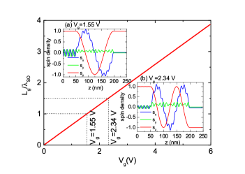
In the main panel of Fig. 6, we have plotted ratio of the gate length to the precession length as a function of gate voltage. The precession length has been calculated as follows: , where . The estimated values of the precession length are of the order of gate length, in particular nm for V and 225 nm for V. We note that in Ref. Fasth et al., 2007 the value of the precession length nm, obtained from the simple modelFasth et al. (2007) used to elaborate the experimental data for the InAs nanowire, is also comparable with the gate length ( nm in Ref. Fasth et al., 2007). Ratio is a linear function of the gate voltage, parametrized as follows: , where V-1. This means that is a decreasing function of the gate voltage in agreement with the experimental data.Dhara et al. (2009) The linear dependence of ratio on allows us to determine the gate voltage that causes the given number of spin rotations performed during the flow of the electron through the nanowire. If , where , the electron spin performs the integer number of rotations [Fig. 6(a)] and the electron does not change its spin on the output. If , the number of electron spin rotations is half integer and the electron changes the spin orientation from the initial (input) value to the final (output) value [Fig. 6(b)]. The number of spin rotations depends on the strength of the SOI that is controlled by the gate voltage.
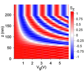
In order to determine the possibilities of the spin manipulation by the gate voltage we have calculated the change of the spin density along the nanowire axis as a function of (Fig. 7). The electrons with spin injected from the source at are detected in the drain at nm. Depending on the gate voltage the detected electrons can have different spins that vary from through to . Only for the suitably chosen gate voltage values the output electrons possess exactly the same spin as the input electrons. For these gate-voltage values the spin transistor is in the on-state. Figure 7 also shows how to choose the gate voltage in order to obtain the output electrons with the opposite spin to that of the injected electrons. If the electrons change their spins in the nanowire, they cannot flow through the device and the spin transistor is in the off-state.
III.2 Comparison with experiment
In this subsection, we present the results of the calculations, which have been motivated by the recent paper of Yoh et al.Yoh et al. (2012) with the InAs nanowire spin transistor. The operation of the spin transistor has been observedYoh et al. (2012) at the room temperature for the InAs nanowire with length m and the gate with length m attached to the nanowire. It is well known that for the nanowire with the length on the order of few m the assumption of the ballistic transport is not satisfied. Nevertheless, we have extended the ballistic transport model beyond the scope of its applicability in order to simulate the spin transistor operation observed in the few-micrometer-long nanowire. The agreement of the calculation results with the experiment can be treated as an a posteriori justification of such extension. The calculations have been carried out for the nanowire with the same geometry as that in Ref. Yoh et al., 2012 and for temperature K. The influence of the temperature has been taken into account only by the Fermi-Dirac distribution of the electrons in the contacts. The electron-phonon scattering has been neglected. In these calculations, we have applied the many-subband approximation, where number of the subbands taken into account was determined by the Fermi-Dirac distribution function [cf. Eq. (25)], and assumed the partial polarization of the electrons in the contacts taking on , which corresponds to the electron spin polarization in Fe electrodes used in the experiment.Yoh et al. (2012) We have treated chemical potential as a fitting parameter and adjusted its value (eV) in order to obtain the best agreement between the calculated and measured current-voltage characteristics for (Fig. 8). The fitting of this single parameter has allowed us to obtain the current-voltage characteristics for other values of the gate voltage (Fig. 8) and current vs gate voltage oscillations (Fig. 9) in a good agreement with the experimental data.Yoh et al. (2012)
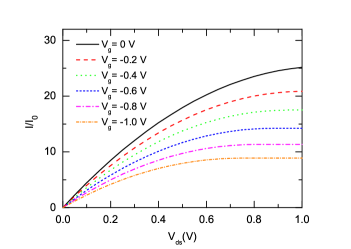
The calculated current-voltage characteristics are plotted in Fig. 8. We see that the curves (Fig. 8) saturate at smaller drain-source voltage if the gate voltage takes on the lower negative values. The value of the saturated current decreases with the decreasing bias voltage. This decrease results from the fact that the lowering of the gate voltage inactivates the subsequent conduction channels, which leads to the drop of the current.
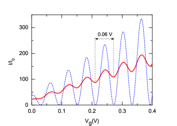
Figure 9 displays the source-drain current as a function of the gate voltage for constant drain-source voltage V. In Fig. 9, we can distinguish the following two current components: the first that monotonically increases with the gate voltage and the second that oscillates as a function of the gate voltage. The monotonically increasing current component results from the activation of the subsequent conduction channels, which occurs when we increase the gate voltage. The oscillating current component results from the SOI induced precession of the electron spin in the vicinity of the gate. The period of oscillations ( V) estimated from Fig. 9 agrees with the measured value.Yoh et al. (2012) The appearance of the oscillating current component can be explained as follows. The total current flowing through the nanowire consists of the two spin-polarized currents with the opposite spin polarization. The contributions of these spin-polarized currents to the total current are not equal to each other, which results from the non-zero spin polarization of the electrons injected from the source [cf. Eqs. (27) and (28)]. This means that the total current flowing through the nanowire is partially spin-polarized [cf. Eq. (29)]. The SOI induced precession of the electron spin in the vicinity of the gate causes that the following pairs of current components: (, ) and (, ) oscillate in anti-phase as a function of the gate voltage. These oscillations lead to the changes of the spin polarization of the current. We note that the spin-polarized current can flow through the drain without any reflection only if the spin polarization of the current is the same as the spin polarization of the electrons in the drain. Therefore, the total current reaches its maximal value for the gate voltage, for which this condition is satisfied. Since the spin-polarized current oscillates as a function of the gate voltage, we obtain the oscillations of the total current on the characteristics (Fig. 9). The amplitude of these oscillations increases with the increasing spin polarization of the electrons in the contacts. Figure 9 also shows that for the full spin polarization of the electrons in the contacts the minimal values of the oscillating current are exactly equal to zero. In Fig. 9, as opposite to Fig. 5(a), the amplitude of the current oscillations increases with the gate voltage, which results from the activation of the subsequent conduction channels.
IV Conclusions and Summary
In the present paper, we have studied the two operation modes of the spin transistor: (A) the ideal operation mode for the zero temperature with the full polarization of electron spins in the contacts and (B) the more realistic operation mode for the room temperature with the partial polarization of electron spins in the contacts. For both the operations modes we have found that the gate-voltage induced SOI leads to the oscillations of the drain-source current as a function of gate voltage. In case (A), the total current stops to flow for the appropriately adjusted gate voltage. In case (B), the total current does not reach zero, but by the tuning of the gate voltage we can obtain the rapid decrease of the total current to its minimal value, which is determined by the spin polarization of the electrons in the contacts. For both the modes we have determined the conditions for the on/off states of the spin transistor in the gated nanowire.
We have also analyzed the spin precession induced by the SOI and demonstrated that this precession results from the superposition of the rotations of and spin components. The estimated precession length is of the order of the gate length and is inversely proportional to the gate voltage. Moreover, we have determined the effect of the spin polarization of electrons in the contacts on the operation of the spin transistor.
In summary, the theoretical description proposed in the present paper allows us to study the physics underlying the operation of the spin transistor in the gated nanowire with the Rashba spin-orbit interaction and provides the computational results in a good agreement with the experimental data.
References
- Datta and Das (1990) S. Datta and B. Das, Appl. Phys. Lett. 56, 665 (1990).
- Bychkov and Rashba (1984) Y. A. Bychkov and E. I. Rashba, J. Phys. C 17, 6039 (1984).
- Matsuyama et al. (2002) T. Matsuyama, C.-M. Hu, D. Grundler, G. Meier, and U. Merkt, Phys. Rev. B 65, 155322 (2002).
- Schmidt et al. (2000) G. Schmidt, D. Ferrand, L. W. Molenkamp, A. T. Filip, and B. J. van Wees, Phys. Rev. B 62, 4790 (2000).
- Slobodsky et al. (2003) A. Slobodsky, C. Gould, T. Slobodskyy, C. R. Becker, G. Schmidt, and L. W. Molenkamp, Phys. Rev. Lett. 90, 246601 (2003).
- Wójcik et al. (2012) P. Wójcik, J. Adamowski, M. Woloszyn, and B. J. Spisak, Phys. Rev. B 86, 165318 (2012).
- Wójcik et al. (2013) P. Wójcik, J. Adamowski, M. Woloszyn, and B. J. Spisak, Appl. Phys. Lett. 102, 242411 (2013).
- Schliemann et al. (2003) J. Schliemann, J. C. Egues, and D. Loss, Phys. Rev. Lett. 90, 146801 (2003).
- Flindt et al. (2006) C. Flindt, A. S. Sorensen, and K. Flensberg, Phys. Rev. Lett. 97, 2405012 (2006).
- Liu et al. (2006) J.-F. Liu, W.-J. Deng, K. Xia, C. Zhang, and Z. Ma, Phys. Rev. B 73, 155309 (2006).
- Fasth et al. (2007) C. Fasth, A. Fuhrer, L. Samuelson, V. N. Golovach, and D. Loss, Phys. Rev. Lett. 98 (2007).
- Liu et al. (2007) J.-F. Liu, Z.-C. Zhong, L. Chen, D. Li, C. Zhang, and Z. Ma, Phys. Rev. B 76, 195304 (2007).
- Ohno and Yoh (2007) M. Ohno and K. Yoh, Phys. Rev. B 75, 241308 (2007).
- Ohno and Yoh (2008) M. Ohno and K. Yoh, Phys. Rev. B 77, 045323 (2008).
- Nazmitdinov et al. (2009) R. G. Nazmitdinov, K. N. Pichugin, and M. Valin-Rodriguez, Phys. Rev. B 79, 193303 (2009).
- Gelabert and Serra (2011) M. M. Gelabert and L. Serra, Eur. Phys. J. B 79, 341 (2011).
- Bringer and Schäpers (2011) A. Bringer and T. Schäpers, Phys. Rev. B 83, 115305 (2011).
- Thorgilsson et al. (2012) G. Thorgilsson, J. Carlos Egues, D. Loss, and S. I. Erlingsson, Phys. Rev. B 85, 045306 (2012).
- Yoh et al. (2012) K. Yoh, Z. Cui, K. Konishi, M. Ohno, K. Blekker, W. Prost, F.-J. Tegude, and J.-C. Harmand, IEEE Xplore Digital Library 2012 70th Annual, 79 (2012).
- Ban and Ya (2013) Y. Ban and S. E. Ya, J. Appl. Phys. 113, 043716 (2013).
- Sadreev and Sherman (2013) A. F. Sadreev and E. Y. Sherman, Phys. Rev. B 88, 115302 (2013).
- Wunderlich et al. (2010) J. Wunderlich, B.-G. Park, C. A. Irvine, L. P. Zarbo, E. Rozkotova, P. Nemec, V. Novak, J. Sinova, and T. Jungwirth, Science 330, 1801 (2010).
- Betthausen et al. (2012) C. Betthausen, T. Dollinger, H. Saarikoski, V. Kolkovsky, G. Karczewski, T. Wojtowicz, K. Richter, and D. Weiss, Science 337, 324 (2012).
- Dhara et al. (2009) S. Dhara, H. S. Solanki, V. Singh, A. Narayanan, P. Chaudhari, M. Gokhale, A. Bhattacharyja, and M. M. Deshmukh, Phys. Rev. B 79, 121311 (2009).