Epitaxial Growth and Electronic Structure of a Layered Zinc Pnictide
Semiconductor, \textbeta-BaZnAs
Abstract
BaZnAs is expected for a good p-type semiconductor and has two crystalline phases of an orthorhombic \textalpha phase and a higher-symmetry tetragonal \textbeta phase. Here, we report high-quality epitaxial films of the tetragonal \textbeta-BaZnAs were grown on single-crystal MgO (001) substrates by a reactive solid-phase epitaxy technique. Out-of-plane and in-plane epitaxial relationships between the film and the substrate were BaZnAs (00l)//MgO (001) and BaZnAs [200]//MgO [200], respectively. The full-widths at half maximum were 0.082o for a 008 out-of-plane rocking curve and 0.342o for a 200 in-plane rocking curve. A step-and-terrace structure was observed by atomic force microscopy. The band gap of \textbeta-BaZnAs was evaluated to be around 0.2 eV, which is much smaller than that of a family compound LaZnOAs (1.5 eV). Density functional theory calculation using the Heyd–Scuseria–Ernzerhof hybrid functionals supports the small band gap.
I Introduction
Layered mixed anion compounds such as LaCuO(S,Se,Te)Ueda et al. (2000, 2001); Hiramatsu et al. (2003, 2002) and La(Fe,Ni)O(P,As)Kamihara et al. (2006, 2008); Watanabe et al. (2008) exhibit a wide variety of electronic functions such as wide band gap high-mobility p-type semiconduction and superconductivity that make them candidates for application as functional materials. In particular, an interesting feature of these compounds is that they have a two-dimensional layered structure composed of a (Cu,Fe,Ni)–(S,Se,Te,P,As) layer and a La–O layer; the former forms a carrier conduction path and the latter has a wider band gap than the conduction layer and behaves like a barrier layer. These compounds with chemical formula LnMOCh (Ln = lanthanide, M = transition metal, Ch = chalcogen) are often called ‘1111-type’ compounds. On the other hand, a similar layered crystal structure called a ‘122-type’ one is reported, which is represented by the chemical formula AeMPn (Ae = alkaline earth, Pn = pnictogen). For the iron pnictide-based superconductors, 122-type AeFePn compounds have widely been investigated due to easiness in growing high-quality epitaxial films compared to the 1111-type ones.Hiramatsu et al. (2008); Katase et al. (2009, 2011)
For semiconductor materials, we have reported that LaMnOPn are anti-ferromagnetic semiconductorsHanna et al. (2013); Kamiya et al. (2010) and LaZnOPn are non-magnetic semiconductors.Kayamura et al. (2007, 2008) There have, however, been only a few reports on 122-type Zn-based compounds AeZnPn;Zhao et al. (2013); Klüfers and Mewis (1978); Hellmann et al. (2007) therefore, we have focused on BaZnAs in this study. We expect a rather large band gap comparable to that of LaZnOAs (1.5 eV).Kayamura et al. (2008) Further, this materials system would be interesting also for other applications; e.g., Zhao et al. synthesized polycrystalline (Ba,K)(Zn,Mn)As for diluted magnetic semiconductors.Zhao et al. (2013)
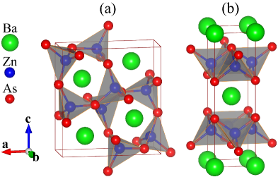
BaZnAs crystallizes into two phases; orthorhombic \textalpha-BaZnAs (\textalpha-BaCuS-type, space group Pnma)Klüfers and Mewis (1978) and tetragonal \textbeta-BaZnAs (ThCrSi-type, space group I4/ mmm),Hellmann et al. (2007) as shown in Fig. 1. The \textalpha-BaZnAs consists of a 3D cage network of (ZnAs) tetrahedrons with a Ba atom encaged in each cage, which is stable at room temperature (RT) – 850 oC. The \textbeta-BaZnAs phase is a typical 122-type one and consists of an alternative stacking of (ZnAs) tetrahedron layers and Ba layers, which is stable at higher temperatures. Since the latter phase has a layered structure, better lateral carrier transport properties are expected in a (001)-oriented epitaxial film.
However, epitaxial growth of \textbeta-BaZnAs is difficult for the following reasons; (1) \textbeta-BaZnAs itself is of a complex structure and a meta-stable phase at RT, and bulk samples are obtained only by a rapid quenching methodHellmann et al. (2007) or heavily extrinsic doping,Zhao et al. (2013) (2) it is difficult to control the stoichiometric composition of BaZnAs because the Zn and As elements evaporate easily at a high temperature but such high temperature is in general necessary for epitaxial growth. For such complex compounds, we have developed a reactive solid-phase epitaxy (R-SPE) method.Hiramatsu et al. (2002); Ohta et al. (2003)
In this work, we report that high-quality epitaxial \textbeta-BaZnAs films were obtained by R-SPE. We also investigated the electronic structure of \textbeta-BaZnAs, but found the band gap is very small (0.2 eV). Hybrid density-functional band calculation supports the small band gap.
II Experimental details
II.1 Target fabrication
Thin films were grown by pulsed laser deposition (PLD). The BaZnAs targets were synthesized through a solid-state reaction from elementary Ba, Zn and As. Ba pieces, fresh Zn powders, and As powders, which were mixed at the stoichiometric ratio, sealed in an evacuated quartz tube, and heated at 700 oC for 20 h. The obtained reaction product was ground, pressed into pellets (8 mm in diameter), and further pressed with a cold isostatic press (CIP) apparatus at 250 MPa. Then, the pellets were sealed in an evacuated quartz tube, reacted at 800 – 900 oC for 20 h, and then furnace-cooled to RT. All the target fabrication processes except for the CIP, the sealing and the heating were conducted in an argon-filled glove box. Besides, stoichiometric amorphous BaZnAs (a-BaZnAs) thin films were quired for R-SPE; therefore, a composition-optimized Zn-rich target (nominal atomic ratio is Ba:Zn:As = 1: 4.0: 2.5) was fabricated by almost the same way except for a lower annealing temperature for the pellet (500 oC) to avoid Zn precipitation.
II.2 Thin film growth
First, we tried to grow epitaxial \textbeta-BaZnAs films on MgO (001) substrates by a simple PLD method using a KrF excimer laser (\textlambda = 248 nm; pulse duration = 20 ns; repetition frequency = 10 Hz). However, the obtained thin films incorporated little Zn when the substrate temperatures (T) were 350 oC, irrespective of varying process parameters including laser power, target composition and vacuum pressure. On the other hand, the films deposited at T < 350 oC were always amorphous and of Zn-poor (e.g., the Ba:Zn:As atomic ratio was 24.6: 29.7: 45.7% for RT deposition) when a stoichiometric target was used. Besides, simple post-deposition annealing of a-BaZnAs films at a high temperature led to a solid-phase epitaxial growth, but their quality was fairly poor.
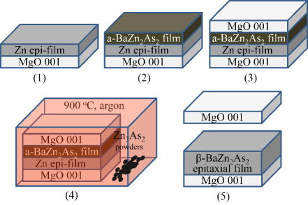
Then, we examined the R-SPE method as illustrated in Fig. 2. Firstly, a metallic Zn layer ( 5 nm in thickness) was deposited on a single-crystal MgO (001) at RT by PLD, followed by deposition of an a-BaZnAs layer (the Ba:Zn:As atomic ratio was 18.9: 41.4: 39.7%) at RT in the same PLD chamber using the optimized target with Ba:Zn:As = 1: 4.0: 2.5. Next, the a-BaZnAs/Zn/MgO sample was covered by an MgO (001) plate, sealed in an argon-filled stainless steel tube, and annealed at 900 oC for 30 min. A small amount of ZnAs powder was contained in the stainless steel tube to suppress the evaporation of the Zn and As elements during the post-annealing process.
II.3 Characterization
X-ray diffraction (XRD) patterns of the bulk samples were measured with a conventional powder XRD instrument (RINT2500, Rigaku). Crystalline quality and orientation of the grown films were examined with a high-resolution XRD (HR-XRD) instrument (Smart Lab, Rigaku). Out-of-plane (2\texttheta\textchi/\textomega synchronous scan) and in-plane (2\texttheta\textchi/\textphi synchronous scan) XRD patterns were measured to determine epitaxial relationships between the films and the MgO substrates and to calculate lattice parameters. Out-of-plane rocking curve (2\texttheta-fixed \textomega scan) and in-plane rocking curve (2\texttheta\textchi-fixed /\textphi scan) were measured to evaluate epitaxial quality of the films. Surface morphology was observed by atomic force microscope (AFM) (SPI-3700, SII). Chemical compositions were determined by X-ray fluorescence (ZSX-100e, Rigaku) with a polycrystalline sample as a reference. Optical absorption spectra from ultraviolet to near-infrared region were recorded in air using a conventional spectrophotometer (U4100, Hitachi), and those in the mid-infrared region were performed in vacuum with a Fourier transform infrared (FTIR) spectrometer (Vertex 70v, Bruker).
II.4 Band structure calculation
Band structures were calculated by density functional theory (DFT) using a code VASP 5.3.3.Kresse and Furthmüller (1996) We first employed Perdew–Burke–Ernzerhof (PBE96) general gradient approximation (GGA) functionals,Perdew et al. (1996) but found that it underestimated the band gap and gave a negative value. We then examined hybrid functionals and found the Heyd–Scuseria–Ernzerhof (HSE) hybrid functionalsHeyd et al. (2003, 2006) with the standard mixing parameter of 25% for the exact-exchange term, because we confirmed that HSE provided a reasonable result for a family compound, LaZnOAs.
III Results and discussion
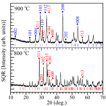
The XRD patterns of BaZnAs bulk samples are shown in Fig. 3. One synthesized at 800 oC was of single-phase \textalpha-BaZnAs (PDF card # 01-071-1811). That synthesized at 900 oC was mostly the \textbeta-BaZnAs phase (# 01-076-5124) with a small amount of the \textalpha-BaZnAs phase. This is consistent with the previous reports and it is hard to obtain a pure \textbeta-BaZnAs phase without some special methods such as the quenching method described in Ref Hellmann et al. (2007).
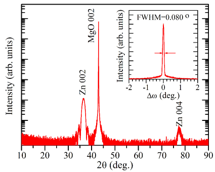
A typical out-of-plane XRD pattern of an a-BaZnAs/Zn bilayer grown on a MgO (001) substrate at Rt is shown in Fig. 4. Only intense Zn 002 and 004 diffraction peaks together with a MgO 002 diffraction peak were observed, indicating the BaZnAs layer was amorphous, while the Zn layer was grown with (001) preferential orientation. The full-width at half maximum (FWHM) of the out-of-plane rocking curve for the Zn 002 diffraction (inset to Fig. 4) was 0.080o, indicating high-quality epitaxial growth.
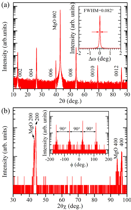
In Fig. 5 the out-of-plane (a) and in-plane (b) HR-XRD patterns of the BaZnAs thin film fabricated by R-SPE after annealing at 900 oC are shown. In the out-of-plane XRD pattern, only intensive \textbeta-BaZnAs 00l and MgO 001 diffraction peaks were observed, indicating the Zn thin layer was sacrificed, and the \textbeta-BaZnAs phase, which is meta-stable at RT in bulk, was obtained. The ultrathin epitaxial Zn layer played as an epitaxy ‘initializer’, which is similar to an epi-ZnO layer for InGaO(ZnO) in RefOhta et al. (2003) and an epi-Cu layer for LaCuOS in RefHiramatsu et al. (2002). The FWHM of the out-of-plane rocking curve for the BaZnAs 008 diffraction (inset of Fig. 5(a)) was 0.082o, indicating a very small tilting. In the in-plane HR-XRD pattern in Fig. 5(b), only BaZnAs 200 and 400 diffraction peaks together with MgO 200 and 400 diffraction peaks were observed. The in-plane rocking curve for 200 diffraction of BaZnAs (inset of Fig. 5(b)) exhibited a four-fold symmetry, consistent with the tetragonal symmetry of \textbeta-BaZnAs (I4/mmm). The average FWHM of the four in-plane 200 rocking curves was 0.342o, indicating a small twisting. The lattice parameters calculated from the out-of-plane and in-plane patterns are listed in Table 1. All the XRD results indicate that high-quality epitaxial \textbeta-BaZnAs thin films were obtained with the epitaxial relationship of out-of-plane BaZnAs (00l)//MgO (001) and in-plane BaZnAs (200)//MgO (200).
| Parameters | Bulk or powders111PDF card: #01-076-5124 | Epitaxial film | Derivation (%) |
|---|---|---|---|
| a (Å) | 4.1200 | +0.18 | |
| c (Å) | 13.5780 | –0.30 | |
| V (Å3) | 230.4784 | +0.11 |
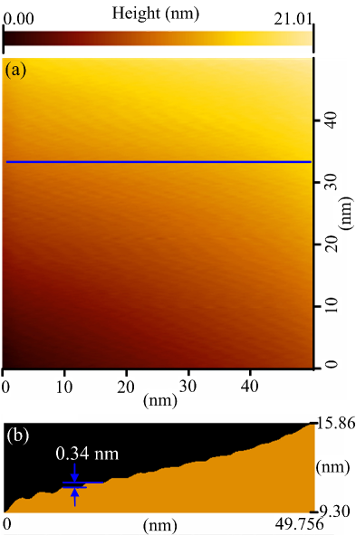
A typical AFM image of the epitaxial film is shown in Fig. 6. It is confirmed that the surface was constructed by a step-and-terrace structure. The step height was 0.34 nm (Fig. 6(b)), nicely agreeing with one fourth of the c-axis length c/4 (c = 1.3578 nm). The origin of this c/4 step height is not clear, but it would correspond to a single Ba layer and a single (ZnAs) layer.
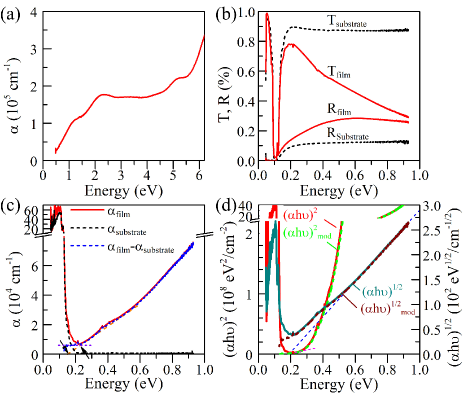
The optical absorption spectrum of the epitaxial \textbeta-BaZnAs film measured by a conventional spectrophotometer is shown in Fig. 7(a). It exhibited a strong absorption band starting from 4.5 eV and a very long plateau in 2 – 4.5 eV. An absorption edge was observed at <1.0 eV; but the absorption coefficient (\textalpha) didn’t vanish to zero or reach a minimum until 0.5 eV, suggesting the band gap should be less than 0.5 eV. To evaluate the band gap for \textbeta-BaZnAs, we further measured FTIR spectra in the lower energy region from 0.04 eV to 0.93 eV. The transmittance and reflectance spectra and the estimated absorption spectrum are shown in Figs. 7(b) and (c), respectively. A strong absorption peak is observed in 0.05 – 0.20 eV for the film/substrate sample. It is caused by the absorption from the MgO substrate (shown by the black dashed lines in Figs. 7(b) and (c)). This absorption hinders the band gap determination more or less. By subtracting the absorption spectrum of the MgO substrate \textalphasubstrate, we plot the net absorption of the film \textalphafilm–\textalphasubstrate by the blue dashed line, showing that an absorption edge would be at 0.23 eV. We also examined a (\textalphah\textnu)2 – h\textnu plot for direct transition and a (\textalphah\textnu)1/2 – h\textnu plot for indirect transition in Fig. 7(d); however, we cannot find a good linear region for these plots. Even so, both plots provide extrapolated values of 0.18 – 0.20 eV. All the above results suggest that the band gap of \textbeta-BaZnAs should be around 0.2 eV, which is much smaller than that of a family compound LaZnAsO with the band gap of 1.5 eV.Kayamura et al. (2008)
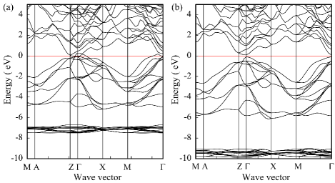
We also performed band structure calculations for the tetragonal \textbeta-BaZnAs. First, we employed PBE96 GGA functionals, but it gave a negative band gap structure as seen in Fig. 8(a). This is caused by a well-known band gap problem of DFT in which band gaps are in general underestimated from experimental values. Then, we examined hybrid functional calculations using HSE as shown in Fig. 8(b). It gives the band gap of 0.2 eV at the \textGamma point as a direct-transition one. The HSE band gap value seems to explain the optical absorption results in Fig. 7(c) and (d).
IV Conclusions
High-quality epitaxial \textbeta-BaZnAs films were grown on MgO (001) substrates by the R-SPE method. The obtained phase was meta-stable high-symmetry tetragonal phase (I4/mmm). The epitaxial relationship was BaZnAs (00l)//MgO (001) (in-plane) and BaZnAs [200]//MgO [200] (out-of-plane). High crystalline quality was confirmed by the small tilting angle of 0.082o and the small twisting angle of 0.342o. The band gap of \textbeta-BaZnAs was estimated to be around 0.2 eV from the FTIR spectra and the HSE calculation.
Acknowledgements.
This work was conducted under Tokodai Institute for Element Strategy (TIES) funded by MEXT Elements Strategy Initiative to Form Core Research Center.References
- Ueda et al. (2000) K. Ueda, S. Inoue, H. Kawazoe, and H. Hosono, Appl. Phys. Lett. 77, 2701 (2000).
- Ueda et al. (2001) K. Ueda, S. Inoue, and H. Hosono, Appl. Phys. Lett. 78, 2333 (2001).
- Hiramatsu et al. (2003) H. Hiramatsu, K. Ueda, H. Ohta, M. Hirano, T. Kamiya, and H. Hosono, Appl. Phys. Lett. 82, 1408 (2003).
- Hiramatsu et al. (2002) H. Hiramatsu, K. Ueda, H. Ohta, M. Orita, M. Hirano, and H. Hosono, Appl. Phys. Lett. 81, 598 (2002).
- Kamihara et al. (2006) Y. Kamihara, H. Hiramatsu, M. Hirano, R. Kawamura, H. Yanagi, T. Kamiya, and H. Hosono, J. Am. Chem. Soc. 128, 10012 (2006).
- Kamihara et al. (2008) Y. Kamihara, T. Watanabe, M. Hirano, and H. Hosono, J. Am. Chem. Soc. 130, 3296 (2008).
- Watanabe et al. (2008) T. Watanabe, H. Yanagi, Y. Kamihara, T. Kamiya, M. Hirano, and H. Hosono, J. Solid State Chem. 181, 2117 (2008).
- Hiramatsu et al. (2008) H. Hiramatsu, T. Katase, T. Kamiya, M. Hirano, and H. Hosono, Appl. Phys. Express 1, 101702 (2008).
- Katase et al. (2009) T. Katase, H. Hiramatsu, H. Yanagi, T. Kamiya, M. Hirano, and H. Hosono, Solid State Commun. 149, 2121 (2009).
- Katase et al. (2011) T. Katase, H. Hiramatsu, V. Matias, C. Sheehan, Y. Ishimaru, T. Kamiya, K. Tanabe, and H. Hosono, Appl. Phys. Lett. 98, 242510 (2011).
- Hanna et al. (2013) T. Hanna, S. Matsuishi, K. Kodama, T. Otomo, S. Shamoto, and H. Hosono, Phys. Rev. B 87, 020401 (2013).
- Kamiya et al. (2010) T. Kamiya, H. Yanagi, T. Watanabe, M. Hirano, and H. Hosono, Mater. Sci. Eng. B 173, 239 (2010).
- Kayamura et al. (2007) K. Kayamura, H. Hiramatsu, M. Hirano, R. Kawamura, H. Yanagi, T. Kamiya, and H. Hosono, Phys. Rev. B 76, 195325 (2007).
- Kayamura et al. (2008) K. Kayamura, R. Kawamura, H. Hiramatsu, H. Yanagi, M. Hirano, T. Kamiya, and H. Hosono, Thin Solid Films 516, 5800 (2008).
- Zhao et al. (2013) K. Zhao, Z. Deng, X. Wang, W. Han, J. Zhu, X. Li, Q. Liu, R. Yu, T. Goko, B. Frandsen, L. Liu, F. Ning, Y. Uemura, H. Dabkowska, G. Luke, H. Luetkens, E. Morenzoni, S. Dunsiger, A. Senyshyn, P. Böni, and C. Jin, Nat. Commun. 4, 1442 (2013).
- Klüfers and Mewis (1978) P. Klüfers and A. Mewis, Z. Naturforsch. 33b, 151 (1978).
- Hellmann et al. (2007) A. Hellmann, A. Löhken, A. Wurth, and A. Mewis, Z. Naturforsch.. 62b, 155 (2007).
- Ohta et al. (2003) H. Ohta, K. Nomura, M. Orita, M. Hirano, K. Ueda, T. Suzuki, Y. Ikuhara, and H. Hosono, Adv. Funct. Mater. 13, 139 (2003).
- Kresse and Furthmüller (1996) G. Kresse and J. Furthmüller, Phys. Rev. B 54, 11169 (1996).
- Perdew et al. (1996) J. Perdew, K. Burke, and M. Ernzerhof, Phys. Rev. Lett. 77, 3865 (1996).
- Heyd et al. (2003) J. Heyd, G. Scuseria, and M. Ernzerhof, J. Chem. Phys. 118, 8207 (2003).
- Heyd et al. (2006) J. Heyd, G. Scuseria, and M. Ernzerhof, J. Chem. Phys. 124, 219906 (2006).