Adam B. Cahaya
Institute for Materials Research, Tohoku University, Sendai 980-8577, Japan
O. A. Tretiakov
Institute for Materials Research, Tohoku University, Sendai 980-8577, Japan
Gerrit E. W. Bauer
Institute for Materials Research and WPI-AIMR, Tohoku University, Sendai
980-8577, Japan
Kavli Institute of NanoScience, TU Delft Lorentzweg 1, 2628 CJ Delft, The
Netherlands
Abstract
We derive expressions for the efficiency and figure of merit of two spin
caloritronic devices based on the spin Seebeck effect (SSE), i.e. the
generation of spin currents by a temperature gradient. The inverse spin Hall
effect is conventionally used to detect the SSE and offers advantages for
large area applications. We also propose a device that converts spin current
into electric one by means of a spin-valve detector, which scales favorably
to small sizes and approaches a figure of merit of 0.5 at room temperature.
Thermoelectric phenomenaSakata2005 transform heat currents into
electric power and vice versa. The Seebeck effect refers to the generation
of an electromotive force (emf) by a temperature gradient,Seebeck1823 while
the production of a heat current by an applied charge current is called
Peltier effect.Peltier Thermoelectric power generators convert waste
heat into electric energy with many potential applications.Vining2009 ; Heremans2013 The spin degree of freedom adds functionalities
and may improve the efficiency of conventional thermoelectric devices.Bauer2012 The spin Seebeck effect (SSE) in the “longitudinal” configuration based on a ferromagnetic
insulatorUchida10 (FI) is especially promising. The SSE converts a
temperature difference between the FI and a normal metal (N) contact into
electric powerXiao10 ; Xiao10a by pumping a spin current into the
normal metal that in turn is converted into a transverse emf by the inverse
spin Hall effectHoffmann (ISHE). The output power is proportional to
the device area perpendicular to the temperature gradient. This scaling
offers the opportunity to generate electricity by large-area coatings using
cheap materials.Kirihara12 Since here the paths of the charge and
heat currents are perpendicular to each other, alternative strategies to
enhance thermoelectric efficiency can be pursued.
In this Letter we validate the efficiency of SSE based power generators. In
addition to considering a device using the ISHE spin charge conversion, we propose harvesting electrical energy by a spin valve spin-filtering mechanism employing metallic ferromagnets. The spin-valve
based SSE power generator scales advantageously for the thermoelectric power
generation in small structures, and multiple elements can be easily added
for a higher output voltage, analogously to conventional thermopiles.
Thermoelectric generators produce electric power by the heat current that
flows between hot and cold reservoirs at temperatures and
respectively. Its efficiency is a monotonic function of the dimensionless
figure of merit where is the average temperature .Sakata2005 When , where
is the maximum possible “Carnot” efficiency. Here we derive and for the two
types of generators driven by the SSE, taking into account the difference of
the physical mechanism between the SSE and conventional thermoelectrics.Bauer2012
In the spin Seebeck effect, the spin current flowing through the interface
is caused by an imbalance of the spin pumping current due to magnetic
thermal noise , that is proportional to FI’s magnon temperature , and a fluctuating spin current caused by thermal
(Johnson-Nyquist) noise in the normal metal that is
proportional to N’s electron temperature.Foros ; Xiao09 Both currents
on average are polarized parallel to the magnetization direction () and cancel each other at equilibrium. The net SSE spin current
reads (indicating time average by ):Xiao10
(1)
where is the interfacial
response function, is the gyromagnetic ratio, is the real
part of spin mixing conductance, is the Boltzmann constant,
is the saturation magnetization, is the magnitude of electron’s charge,
and is a magnetic coherence volume that depends on spin wave
stiffness and weakly on temperature.Xiao10a Adachi et al.Adachi11 and Hoffman et al.Hoffman13 derived similar
expressions by different methods. The magnitude of the real part of the
mixing conductance is well established for intermetallic interfacesBrataas06 as well as interfaces with magnetic insulators.Jia11 ; Burrowes12 ; weiler13
The interface temperature discontinuity depends sensitively on the device
and material parameters.Schreier13 In the limit of small interface
heat resistance, the phonon temperature is continuous and governed by the
coupled heat diffusion equation for the bilayer with many not very
well-known parameters.Sanders77 ; Xiao10 ; Schreier13 Here we assume, for
simplicity, a dominating thermal boundary resistance
(Kapitza resistanceKapitza41 ), such that the magnon and phonon
temperatures in the FI at the interface are
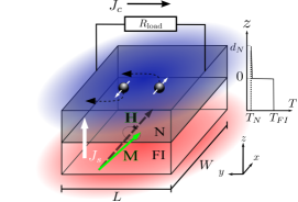
approximately the same,Agrawal12 ; Schreier13 , see Fig. 1. In this limit
(2)
where is the electron (and phonon) temperature of the normal metal
at and is the heat current through the interface. Since
the spin contribution to the interface heat transport is comparably small,
the Kapitza resistance is dominated by phonon transport.Xiao10 ; Schreier13
The heat flow through the system is partly converted into a spin current at
the interface that subsequently has to be transformed into electric energy. The
coupling between heat and spin over the FIN interface can be written in
the form of a linear response matrix relation to the driving forces, viz. the spin accumulation in the normal metal and temperature
difference leading to the spin and averaged
heat current responses:
(3)
Here is the interface spin injection conductance, Bender ; Jiao
that generates backflow of the spin Seebeck spin current,
is the spin
Seebeck coefficient, and is the Kapitza conductance (inverse of the Kapitza resistance ).
The spin current is positive when and , so . The spin Peltier coefficient due to
Onsager reciprocity, where .
Figure 1: (Color online) A schematic view of the spin Seebeck power generator based
on the inverse spin Hall effect (ISHE). A bilayer of ferromagnetic insulator and normal metal with a low interface heat conductance pumps a spin current into N. Then is converted into a transverse charge current by means of the ISHE.
We first consider the efficiency of a SSE generator with spin-charge
conversion by the ISHE when connected to an external load resistance that utilizes the electric energy. The basic setup is shown
in Fig. 1. Eq. (3) defines the spin and heat currents
through the FIN interface. The transverse electric current density generated by the ISHE inside N at distance from interface is
(4)
where is the spin-current density
direction vector (in units of A/m2), is its
polarization, and is the spin Hall angle. For the charge current and emf are and . In the presence of spin flips, a
spin accumulation profile builds up at the interface. It obeys the
spin-diffusion equation ,
where is the spin-flip diffusion length in N. The charge and spin current densities in N therefore read
(5)
Spin current conservation at the boundaries gives from Eq. (3) and , where is the length of N in the direction of the ISHE current, and
is the width of the FIN bilayer (see Fig. 1). The solution
of the spin-diffusion equation
(6)
depends on the spin conductance and the
induced transverse voltage . The integrated
transverse charge current in N then reads
(7)
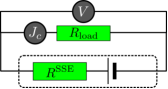
Figure 2: (Color online) An effective circuit for the spin Seebeck power generators with internal
resistance . Current and voltage on external
load with are measured by ideal volt and ampere meters.
The SSE generator is a battery with internal resistance and a maximum output voltage , Cahaya2013 see Fig. 2, that is
(8)
(9)
(10)
The voltage drop over the load resistance is
(11)
The thermally generated electric power dissipated in the load resistance
(12)
scales with the device area . The maximum output voltage when is
proportional to the sample length . for large since the emf is short-circuited by the
non-active conducting region. When the voltage output
vanishes with the gradient of the spin accumulation.
The efficiency can be expressed in a form similar to conventional thermoelectrics, Sakata2005
(13)
in terms of figure of merit that can be obtained by maximizing with respect
to , i.e. by impedance matching, leading to
(14)
Here the thickness for the optimal spin-charge
conversion is given by the (positive) solution of the equation
(15)
We can now estimate the figure of merit for the yttrium iron garnet (YIG)Pt system . The spin Seebeck coefficient has
the universal value Jiao Withweiler13 m-2 we find (here and in the following at room temperature) AK-1m-2. The spin conductance governs the spin current injected back into FI by the
spin accumulation and is estimated for the YIGPt interface to be i.e.
much smaller than the spin conductance of Pt: mforweiler13 and Limit leads to the
simplification
(16)
It shows that is
invariant with respect to the sample area. We can estimate its value usingweiler13 and
as well as the phonon contribution to the Kapitza conductanceSchreier13 Wm-2K which corresponds to about 40 nm of bulk YIG and is larger than
the spin contributionSchreier13 . This leads to and for the optimum width of .
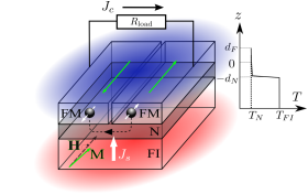
We now turn to the alternative SSE power generator in which the thermal
spin-motive force generates an electromotive force by means of ferromagnetic
metal (FM) contacts, viz. by the spin valve effect. The N layer is
now a metal with a long spin-flip diffusion length such as Cu. As shown in
Fig. 3, the spin current in this case is injected into the N
layer of a lateral metallic spin valve with ferromagnetic contacts in an
antiparallel configuration collinear to the magnetization of the magnetic
insulator. The spin accumulation injected thermally into the N spacer
therefore generates a voltage difference between the contacts. The FMN
contact areas are and that of the FIN contact is approximately .
Figure 3: (Color online) A schematic view of the spin-valve based spin Seebeck power
generator. Two antiparallel ferromagnetic layers (FM) are added to the FIN bilayer device in Fig. 1. The spin accumulation in N drives a charge current through the metallic spin valve, thereby generating a voltage over the load resistance.
We assume that the spin-flip diffusion length is larger than the sample
dimensions such that the spin accumulation is constant in N. The charge-spin
linear response relations at the interface of the NFM interface with
conductance (including the magnetically active thickness of the bulk
ferromagnet) can be written as
(17)
where is the spin polarization of the NFM contact, and are the electrochemical potential and
spin accumulation in N, and are the electrochemical potential and
spin accumulation in FM, and the superscript corresponds to a
contact with magnetization parallel () or antiparallel () to that of
the FI.
Assuming zero spin accumulation on the other side of the FM contact and
conservation of spin current in N, :
(18)
(19)
where the induced voltage . The effective electric
circuit for the spin-valve based generator is again given by Fig. 2 with internal resistance and
maximum voltage :
(20)
(21)
The optimal figure of merit
is obtained again by maximizing the efficiency with
respect to :
In the limit of a half-metal, this expression appears to diverge, but when
we first take and then :
(24)
the result looks similar to the figure of merit for conventional thermoelectrics.
The numerical estimate is obtained forSchreier13 m-2K-1 andweiler13 m-2.
To summarize, we consider two schemes of thermoelectric power
generators based on the spin Seebeck effect. We estimate their figures
of merit under the assumption that the total heat
conductance is limited by the FIN interface.
This assumption importantly simplifies the model, but since the Kapitza interface conductance has not yet been measured for YIGmetal interfaces, also introduces uncertainties. The output voltage of the
SSE-ISHE device is proportional to sample length perpendicular to the
FI’s magnetization and temperature gradient (Fig. 1), while
the power scales with the area. Therefore this scheme has an advantage for
large area devices, but
is small since it is limited by . A spin valve can convert spin into charge current
as well, offering the possibility to enhance
considerably. The scale independence of the output voltage in spin-valve SSE
devices can be useful for micro- and nanoscale applications, since the
output voltage does not decrease when down-scaling the device. Experiments
demonstrating the SSE by a spin valve are highly desirable since they would
shed light on the role of interface proximity or spin-orbit interaction
effects that might exist for YIGPt but not for YIGCu.Huang The present modelling is also applicable for other devices, such as spin Seebeck-assisted magnetic random access memories.Mojum
We thank E. Saitoh, K. Uchida, J. Flipse, and J. Xiao for insightful
discussions. A.B.C. is supported by Japanese Ministry of Education Culture,
Sports, Science and Technology (MEXT) Scholarship Grant. We acknowledge
support by the Grants-in-Aid for Scientific Research (Nos. 25800184, 25220910, and
25247056), the DFG via SPP 1538 “Spin Caloric
Transport”, the EU RTN Spinicur and DAAD SpinNet.
References
(1) M. Sakata, Thermoelectric Energy Conversion:
Theory and Applications (Shokabo, Tokyo, 2005).
(2) T. J. Seebeck, Abh. Dtsch. Akad. Wiss. Berlin 265, 1822 (1823).
(3) J. C. Peltier, Ann. Chim. 56, 371 (1834).
(4) C. B. Vining, Nature Mater. 8, 83 (2009).
(5) J. P. Heremans, M. S. Dresselhaus, L. E. Bell, and D.
T. Morelli, Nature Nanotech. 8, 471 (2013).
(6) G. E. W. Bauer, E. Saitoh, and B.J. van Wees, Nature
Mater. 11, 391 (2012).
(7) K. Uchida, J. Xiao, H. Adachi, J. Ohe, S. Takahashi, J.
Ieda, T. Ota, Y. Kajiwara, H. Umezawa, H. Kawai, G. E. W. Bauer, S. Maekawa,
and E. Saitoh, Nature Mat. 9, 894 (2010).
(8) J. Xiao, G. E. W. Bauer, K. Uchida, E. Saitoh, and
S. Maekawa, Phys. Rev. B 81, 214418 (2010).
(9) J. Xiao, G. E. W. Bauer, K. Uchida, E. Saitoh, and
S. Maekawa, Phys. Rev. B 82, 099904 (E) (2010).
(10) For a review see: A. Hoffmann, IEEE Trans. Magn.
49, 5172 (2013)
(11) A. Kirihara, K. Uchida, Y. Kajiwara, M. Ishida,
Y. Nakamura, T. Manako, E. Saitoh, and S. Yorozu, Nature Mater. 11,
686 (2012).
(12) J. Foros, A. Brataas, Y. Tserkovnyak, and G. E. W. Bauer,
Phys. Rev. Lett. 95, 016601 (2005).
(13) J. Xiao, G. E. W. Bauer, S. Maekawa, and A. Brataas, Phys.
Rev. B 79, 174415 (2009).
(14) H. Adachi, J. Ohe, S. Takahashi, and S. Maekawa, Phys.
Rev. B 83, 094410 (2011).
(15) S. Hoffman, K. Sato, and Y. Tserkovnyak, Phys. Rev. B
88, 064408 (2013).
(16) A. Brataas, G. E. W. Bauer, and P. J. Kelly, Phys. Rep.
427, 157 (2006).
(17) X. Jia, K. Liu, K. Xia, and G. E. W. Bauer, Europhys. Lett.
96, 17005 (2011).
(18) C. Burrowes, B. Heinrich, B. Kardasz, E.A. Montoya,
E. Girt, Y. Sun, Y.-Y. Song, and M. Wu, Appl. Phys. Lett. 100,
092403 (2012).
(19) M. Weiler, M. Althammer, M. Schreier, J. Lotze, M.
Pernpeintner, S. Meyer, H. Huebl, R. Gross, A. Kamra, J. Xiao, Y. Chen, H.
Jiao, G.E.W. Bauer, and S.T.B. Goennenwein, Phys. Rev. Lett. 111,
176601 (2013).
(20) M. Schreier, A. Kamra, M. Weiler, J. Xiao,
G.E.W. Bauer, R. Gross, and S.T.B. Goennenwein, Phys. Rev. B 88,
094410 (2013).
(21) D. J. Sanders and D. Walton, Phys. Rev. B 15,
1489 (1977).
(22) G. L. Pollack, Rev. Mod. Phys. 41, 48 (1969).
(23) M. Agrawal, V. I. Vasyuchka, A. A. Serga, A. D.
Karenowska, G. A. Melkov, and B. Hillebrands, Phys. Rev. Lett. 111,
107204 (2013).
(24) S. A. Bender, R. A. Duine, and Y. Tserkovnyak, Phys. Rev.
Lett. 108, 246601 (2012).
(25) H. Jiao, J. Xiao, and G.E.W. Bauer, (unpublished).
(26) A. B. Cahaya, O. A. Tretiakov, and G.E.W. Bauer,
(unpublished).
(27) J. Hamrle, T. Kimura, Y. Otani, K. Tsukagoshi, and Y.
Aoyagi, Phys. Rev. B 71, 094402 (2005).
(28) S. Y. Huang, X. Fan, D. Qu, Y. P. Chen, W. G. Wang, J. Wu,
T. Y. Chen, J. Q. Xiao, and C. L. Chien, Phys. Rev. Lett. 109,
107204 (2012).
(29) N.N. Mojumder, D.W. Abraham, K. Roy, and D.C. Worledge, IEEE
Trans. Magn. 48, 2016 (2012).