Band gap engineering in graphene and hexagonal BN antidot lattices: A first principles study
Abstract
Effects of antidot lattices on electronic structures of graphene and hexagonal BN (h-BN) are investigated using the first principles method based on density functional theory. For graphene, we find that when the antidot lattice is along the zigzag direction, the band gap opening can be related to the inter-valley scattering, and does not follow the simple scaling rule previously proposed in literature for the antidot lattice along the armchair direction. For h-BN, our calculations show that the antidot lattice results in reducing of band gaps. Coupled with doping of carbon atoms, the band gap of an h-BN antidot lattice can be reduced to below 2 eV, which might have implications in light-emitting devices or photoelectrochemistry.
Graphene and hexagonal BN (h-BN) have the same two-dimensional (2-d) honeycomb lattice, but drastically different electronic properties: Graphene is a gapless semimetal due to the symmetry between two sublattices of the honeycomb structure, while h-BN is a semiconductor with a wide band gap (around 5.5 eV Song et al. (2010)) because of the lack of such symmetry. Recently, band gap engineering of these two materials has become a subject of intensive research in the context of nanoscale electronics Geim and Novoselov (2007); Ci et al. (2010). Many interesting ways have been proposed and investigated to tune the band gap of graphene or h-BN based materials, such as further reducing the material’s dimensionality to form nanoribbons Nakada et al. (1996); Son, Cohen, and Louie (2006); Han et al. (2007), applying external superlattice potential Tiwari and Stroud (2009), decorating the material with different chemical species (for example, hydrogenation) Elias et al. (2009); Singh and Yakobson (2009); Balog et al. (2010), and the mixture of these two materials Ci et al. (2010). Quite recently, based on a tight-binding approach (TB), T. G. Pederson et al. suggested that introducing antidot lattice structure into graphene may be an effective way to turn graphene from semimetal to semiconductor Pedersen et al. (2008). In their study, for graphene antidot lattices consisting of a triangular array of holes along the armchair direction (armchair antidot lattices), a simple scaling rule for band gaps was proposed, , where is the total number of carbon atoms in pristine graphene in one supercell, and is the number of carbon atoms removed in the same cell from the pristine graphene to form the corresponding antidot lattice.
In this paper, first, we investigated electronic structures of another type of graphene antidot lattices that consists of holes along the zigzag direction (zigzag antidot lattices). Completely different behaviors of band gaps from those of armchair cases were found. The inter-valley scattering is identified as a crucial factor in the gap opening of graphene antidot lattices and the major reason that causes the differences between zigzag and armchair cases. We then studied effects of antidot lattices on electronic properties of h-BN that has the same 2-d structure but different sublattice symmetry. Interestingly, our calculations suggested that the inter-valley scattering does not have the significant effects on band gaps of h-BN as it does to graphene cases, and the antidot lattice always tends to reduce the band gap of h-BN. With an appropriate band gap, the engineered h-BN antidot lattice might be promising not only as an electronic material but aslo in light-emitting applications or photoelectrochemistry.
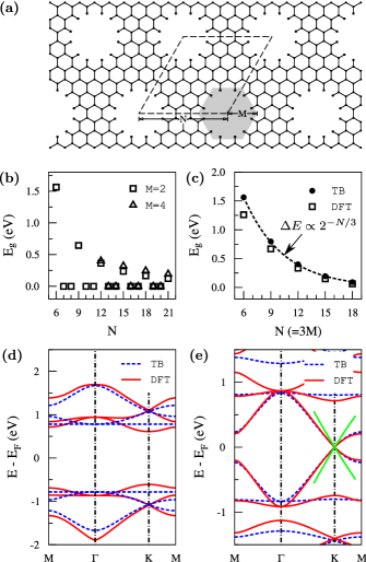
The geometry of graphene antidot lattices studied in this paper is illustrated in Fig. 1(a). The antidots considered in this study form a triangular lattice and have a hexagonal shape (as grayed), which is commonly observed in oxygen-etched highly orientated polycrystalline graphite (HOPG) Chang and Bard (1990); Chu and Schmidt (1991). We focus on the case that the holes are arranged along the zigzag direction as shown in the figure. In the following, the graphene antidot lattice will be referred to as , where is the supercell lattice constant and is the side length of hexagonal holes. Both and are specified in units of graphene lattice constant, Å. In such a configuration, numbers of carbon atoms in two sublattices are equal. Electronic structures are calculated using both a single-orbital tight-binding (TB) approach Wallace (1947) and density functional theory (DFT). The hopping integral used in TB calculations is -2.7 eV. DFT calculations were performed using the siesta code Sánchez-Portal et al. (1997) with local density approximation and double- polarization basis sets. Results from both TB and DFT calculations agree with each other very well [see Figs. 1(c-e)]. Figure 1(b) shows the dependence of band gaps on the periodicity of holes, , with hole sizes () fixed. We observed in this figure that band gaps open only when is multiples of three. Figure 1(c) shows the variation of band gaps as a function of for the case of . The variation of the band gap in this case can be nicely fitted with as shown in the figure, which is very different from the aforementioned simple scaling rule of armchair antidot lattices. The corresponding correlation coefficient of fitting is 0.97. A comparison between band structures of and configurations is shown in Figs. 1(d, e). The configuration, for which is multiples of three, has a direct band gap at K. The configuration, for which is not multiples of three, preserves the characteristic Dirac cone structure at K, though the Fermi velocity is reduced if compared to pristine graphene. Such periodicity dependence suggests that band gap opening in graphene antidot lattices can be related to the inter-valley scattering between different Dirac points, since when the periodicity is multiples of three, two nonequivalent Dirac points in prinstine graphene coincide with each other due to the Brillouin zone folding and then the inter-valley scattering becomes manifest. If the holes are along the armchair direction, the band gap is always open because in this case, the inter-valley scattering condition is always satisfied. In practice, disorder is inevitable in the fabrication process of graphene antidot lattice. To show effects of disorder, we performed a series of calculations with a 4848 supercell, in which different holes with ranging from 2 to 6 and having an approximate normal distribution of and are present. Our calculations show that disorder will introduce localized states in the bandgap, and the gap between extended state band edges is larger than that of the ordered lattice.
We then turn to antidot lattices in h-BN that has the same 2-d atomic structure as graphene but lacks the sublattice symmetry. The band gap of pure h-BN predicted by DFT is 4.52 eV, which is about 1 eV less than the experimental value of multiple-layer h-BN, 5.5 eV Song et al. (2010). The h-BN antidot lattice is constructed in the same way as the graphene antidot lattice. An example of h-BN antidot lattice is shown in Fig. 2(a). Various kinds of h-BN antidot lattces, , with ranging from 6 to 18 and ranging from 2 to 8, were considered in this paper. As shown in Fig. 2(b), the band gaps of h-BN antidot lattices are always smaller than pure h-BN, and unlike the graphene antidot lattice, there are no significant differences between band gaps of cases and those of ( is an integer), indicating that in h-BN antidot lattices, the inter-valley scattering does not have significant effects on electronic structures as it does to graphene antidot lattices. The band gap variation of h-BN antidot lattices are governed by two trends. Firstly, band gaps of h-BN antidot lattices are overally reduced with the decreased ratio of . That is to say, with fixed, a bigger hole size normally means a smaller band gap, and with fixed, a bigger periodicity , usually brings a bigger band gap. In the Fig. 2(b), the smallest band gap, 3.45 eV, was obtained in h-BN . Secondly, for a fixed ratio, the band gap scales in an inversely proportional manner with respect to the size of unit cell, , as shown in the inset of Fig. 2(b). The band gap scaling behavior is similar if the antidot lattice is along the armchair direction. The fixed-ratio scaling behaviors are quite different between the graphene antidot lattice (Fig. 1(c)) and the h-BN antidot lattice, which suggests different mechanisms of band gap opening for these two materials.

The band gap of h-BN antidot lattices may be further reduced by carbon doping. The carbon doping of h-BN can be done by ion implantation Bangert et al. (2010). The essence of the idea is to mitigate the on-site energy difference between B and N sublattices via random substitution by carbon atoms on both sublattices. We start with a h-BN antidot lattice which has a band gap of 4.03 eV. We find that it is much more energetically favorable by more than 1 eV per atom for carbon atoms to form dimers than to scatter dispersively, which also agrees with experimental findings Kawaguchi, Kawashima, and Nakajima (1996), so only doping with carbon dimers is considered. An example of a configuration with two carbon dimers is shown in Fig. 3(a). For each carbon concentration, which is defined as the ratio between number of carbon atoms and total number of atoms except hydrogen, about 20 random doping configurations are calculated using DFT. The variation of the averaged band gaps with respect to carbon concentration and the corresponding sample standard deviations are shown in Fig. 3(b). It can be seen that the band gap decreases steadily as the concentration of doped carbon dimers increases. A band gap below 2 eV is achievable. The large range of the band gap adjustable by antidot lattices and carbon doping, from 4.5 eV to 2 eV, may have applications in semiconducting electronics, light-emitting devices, and photoelectrochemistry.

In summary, band gap engineering using antidot lattices in graphene and h-BN is discussed. In graphene with antidots along the zigzag direction, we show that band gap opening occurs only when the periodicity is multiples of three, which can be related to the inter-valley scattering. Due to the lack of sublattice symmetry, the inter-valley scattering has no significant effects on band gaps of h-BN antidot lattices as it does to graphene cases. Band gaps of h-BN antidot lattices were found to approximately scale with . We further show that the band gap of an h-BN antidot lattice can be decreased below 2 eV using carbon doping to mitigate the sublattice on-site energy difference. Both methods have their own merits. Carbon doping might be adaptive for mass production, while antidot lattices have the advantage of spatial locality and are suitable for fabricating of atomic-perfect-interface heterostructures on the same sample. These two methods combined appropriately might have important implications in optoelectronics and photoelectrochemistry.
This work was supported by NUS Academic Research Fund (Grant Nos: R-144-000-237133 and R-144-000-255-112).
References
- Song et al. (2010) L. Song, L. J. Ci, H. Lu, P. B. Sorokin, C. H. Jin, J. Ni, A. G. Kvashnin, D. G. Kvashnin, J. Lou, B. I. Yakobson, and P. M. Ajayan, Nano Lett. 10, 3209 (2010).
- Geim and Novoselov (2007) A. K. Geim and K. S. Novoselov, Nat. Mater. 6, 183 (2007).
- Ci et al. (2010) L. Ci, L. Song, C. H. Jin, D. Jariwala, D. X. Wu, Y. J. Li, A. Srivastava, Z. F. Wang, K. Storr, L. Balicas, F. Liu, and P. M. Ajayan, Nat. Mater. 9, 430 (2010).
- Nakada et al. (1996) K. Nakada, M. Fujita, G. Dresselhaus, and M. S. Dresselhaus, Phys. Rev. B 54, 17954 (1996).
- Son, Cohen, and Louie (2006) Y. W. Son, M. L. Cohen, and S. G. Louie, Phys. Rev. Lett. 97, 216803 (2006).
- Han et al. (2007) M. Y. Han, B. Özyilmaz, Y. Zhang, and P. Kim, Phys. Rev. Lett. 98, 206805 (2007).
- Tiwari and Stroud (2009) R. P. Tiwari and D. Stroud, Phys. Rev. B 79, 205435 (2009).
- Elias et al. (2009) D. C. Elias, R. R. Nair, T. M. G. Mohiuddin, S. V. Morozov, P. Blake, M. P. Halsall, A. C. Ferrari, D. W. Boukhvalov, M. I. Katsnelson, A. K. Geim, and K. S. Novoselov, Science 323, 610 (2009).
- Singh and Yakobson (2009) A. K. Singh and B. I. Yakobson, Nano Lett. 9, 1540 (2009).
- Balog et al. (2010) R. Balog, B. Jorgensen, L. Nilsson, M. Andersen, E. Rienks, M. Bianchi, M. Fanetti, E. Laegsgaard, A. Baraldi, S. Lizzit, Z. Sljivancanin, F. Besenbacher, B. Hammer, T. G. Pedersen, P. Hofmann, and L. Hornekaer, Nat. Mater. 9, 315 (2010).
- Pedersen et al. (2008) T. G. Pedersen, C. Flindt, J. Pedersen, N. A. Mortensen, A. P. Jauho, and K. Pedersen, Phys. Rev. Lett. 100, 136804 (2008).
- Chang and Bard (1990) H. P. Chang and A. J. Bard, J. Am. Chem. Soc. 112, 4598 (1990).
- Chu and Schmidt (1991) X. Chu and L. D. Schmidt, Carbon 29, 1251 (1991).
- Wallace (1947) P. R. Wallace, Phys. Rev. 71, 622 (1947).
- Sánchez-Portal et al. (1997) D. Sánchez-Portal, P. Ordejon, E. Artacho, and J. M. Soler, Int. J. Quantum Chem. 65, 453 (1997).
- Bangert et al. (2010) U. Bangert, A. Bleloch, M. H. Gass, A. Seepujak, and J. van den Berg, Phys. Rev. B 81, 245423 (2010).
- Kawaguchi, Kawashima, and Nakajima (1996) M. Kawaguchi, T. Kawashima, and T. Nakajima, Chem. Mat. 8, 1197 (1996).