Conductance in the Helimagnet- and Skyrmion-Lattice-Embedded Electron Waveguide
Abstract
The helimagnet (HM) and skyrmion lattice (SL) are topologically nontrivial magnetic states. Their spin texture gives rise to finite topological magnetic field and Lorentz force. As a demonstration of the emergent electrodynamics besides the Hall effect, the transmission of electrons within a waveguide (WG) embedded with a HM/SL layer is shaped by the topological spin texture. In this work, we investigated the conductance properties in the HM/SL-film-embedded electron WG and found that under translation of the HM/SL layer the conductance contour as a function of the layer center demonstrates nearly identical pattern to the original spin field contour. When an electron transports in the WG, the topological magnetic field generalized by the HM/SL spin texture exerts on it and distorts the wavefunction shape in the - plane. By interference between different quantum paths the electron experiences, the HM/SL spin texture is recorded in the conductance. The scheme also provides a possible detect of the HM/SL spin configuration by transport experiment.
pacs:
72.10.Fk, 75.30.Et, 85.75.-dI Introduction
The helimagnet(HM) is a kind of nontrivial magnetic stateRef13 with its spin spiraling in two or three dimensions characterized by a single spiral wavevector . The skyrmion lattice (SL) is the topologically protected stable spin texture with spin vortices forming two-dimensional hexagonal, triangular, or square crystal structures, which was recently discovered in magnetic metal alloys, insulating multiferroic oxides, and the doped semiconductorsSL1 ; SL2 ; SL5 . Also, a two-dimensional square lattice of skyrmions was found to be the magnetic ground state of a monolayer hexagonal Fe film on the Ir(111) surfaceSL14 . The SL state was first discovered in the chiral HMSL1 . The HM and SL can be generalized into a multi- description with single in HMs and multiple ’s in SLsSL1 ; SL10 ; SL11 . These multi- states have more complex topological properties and Fourier spectra than earlier-discovered ferromagnet, antiferromagnet, and ferrimagnet. Their spin structures can be detected by neutron scatteringSL1 and Lorentz transmission electron microscopySL2 . The Hall effect measurements in the SL metals establish the physics of emergent electrodynamicsSL3 ; SL4 .
When a single electron passes through the HM or spin vortex structure, spin-dependent diffraction occurs bearing information of the spin texture. Recently the transport properties of the HM-embedded devices are targeted from different view angles in literature, which lays foundations for the present approach. Manchon et al.Ref42 and usRef43 observed the spin-dependent diffraction effect in the transmission at the ferromagnet/HM interface and through the thin-layer HM junction, respectively. Some functional devices were proposed based on the HM such as the persistent spin currentsRef19 , spin-field-effect transistorRef17 , tunneling anisotropic magnetoresistanceRef18 , and spin resonanceRef13 . Conductance characteristic of the HM spin configuration and spiral period was found in the Fano resonance spectrum of a quasi-one-dimensional WG containing a thin conducting HM layer as a donor impurityRef52 . While the HM-based structures have been extensively investigated particularly for spintronic exploitationsRef42 ; Ref43 ; Ref19 ; Ref17 ; Ref18 ; Ref52 ; SL12 , scientists are also seeking the potential of the SL in the spintronic arena. Extremely small threshold current to induce spin transfer torque effect was found in bulk SLsSL6 . Till now, research on the transport properties in SL-based structures is in the preliminary level. There remain many unsolved physical problems. Nevertheless, the SL transport properties are important to reveal its fundamental quantum nature and excavate potential detection methods.
Among various transport devices, we take the SL(HM)-embedded waveguide (WG) as our targeting structure. The most important reason is that the separated levels confined in the WG could avoid phase-randomization by the reservoirs in most other schemes. Resonance and Fano resonance phenomena were theoretically observed in two and quasi-one dimensional WGs containing an impurity point or layer, which correlates propagating and evanescent subbands of the WGSL7 ; SL8 ; SL9 ; Ref52 . When an electron interacts with the SL vortex, diffraction occurs as a result of the space-dependent spin exchange coupling. Due to the complex geometric configuration, high-order Fourier components should be included in solving the transmissivity. As a primary transport approach, using the WG minimizes the algebra tediousness and does not lose the main characteristics of the SL-related transport.
In this letter, we investigated the transmission and conductance properties in the HM- and SL-film-embedded two-dimensional rectangular electron WG. It is found that under translation of the magnetic film the conductance as a function of the position demonstrates nearly identical pattern to the original spin contour bearing all the spatial symmetry. The scheme provides a possible detect of the HM and SL configuration by transport experiment. The underlying mechanisms are the topology-shaped electron transport.
II Theoretical formulation
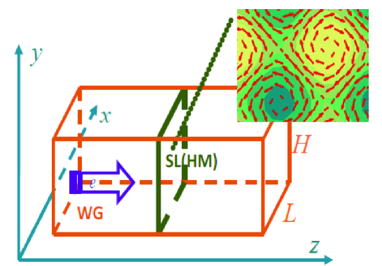
The scheme we propose is a two-dimensional rectangular WG containing a thin-film HM/SL layer acting as a scatterer sketched in Fig. 1. The Schrödinger equation describing scattering in such a device is
| (1) |
The confining potential of the WG is an infinite rectangular well with width and height across the - plane. Its eigenstates and corresponding subband energies are
| (2) |
| (3) |
with and the subband index and the free-electron mass. A rectangular WG is used so that no level degeneracy appears and the third energy level is far above the ground and second energy levels taken into account. We set the incident energy between the first and second subbands of the waveguide with the eigenenergies , and eigenfunctions , .
The spin vector field of the HM and SL can be be described in the multi- pictureSL1 ; SL11 .
| (4) |
with -fold symmetry. In this approach consider , , and , which describes a HM, square and triangular SL, respectively. are spiral wave vectors. and are two unit vectors orthogonal to each other and to . All the helices characterized by have the same chiralitySL1 with .
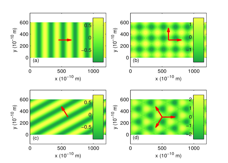
We consider four kinds of spin textures with its spin- component contour depicted in Fig. 2, in which , , and can be expressed as follows which does not lose generality.
| (5) |
| (6) |
| (7) |
Here with the spiral period of a single for the multi- description of the HM and SLs. We investigate the dependence of the transport properties on the HM/SL spin configuration.
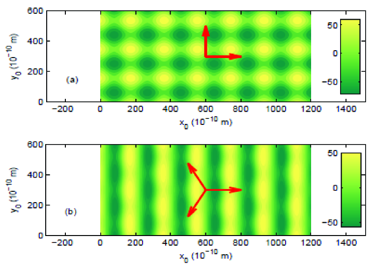
The HM/SL thin film is embedded into the WG. We define the total skyrmion numberSL14
| (8) |
where is the unit vector of the local magnetization defined in Eq. (4). Different from Ref. SL14, , the integral is taken over the WG confined area. A complete skyrmion vortex within the WG contributes one topological number and a partial skyrmion vortex contribute a partial topological number depending on the radius and complete whirling rings within the SL. For HMs, the spiral is open without forming closed winding path hence no Berry phase is accumulated and the skyrmion number is zero.
The localized spin-dependent scattering potential of the thin-film HM/SL layer can be approximated by a Dirac-delta function as
| (9) |
where is the sd-type exchange coupling strength between free electrons and the background spin texture. is the electrostatic potential of the HM/SL. For insulating, semiconducting, and conducting HM/SL materials, is positive and negative correspondingly, which can also be tuned by external electric gates. is the thickness of the HM/SL layer.
Using the waveguide eigenstates as the expanding basis of the wave function , Eq. (1) can be converted to a set of linear equations. In the matrix formalism, the equations areSL7 ; Ref52
| (10) |
where are elements of the diagonal matrix of wave vectors with and is extended to the wave-spin product space. Also, elements of the spin-dependent interband transition matrix
| (11) |
where
| (12) |
are the waveguide eigenfunctions extended to the spin space in the -representation. With both the WG eigenfunctions and the HM/SL spin vector fields (co)sinusoidal functions, can be analytically obtained.
The spin-dependent transmission amplitudes can be obtained from Eq. (10) by matrix algebra. Here denotes transmission amplitudes from the -th subband with spin- polarization to the -th subband with spin- polarization. The spin-dependent conductance can be calculated from the two-terminal Landauer formulaSL7
| (13) |
III Numerical results and interpretations
We consider the transport properties of the HM/SL-embedded two-dimensional rectangular electron WG. We varies the position of the HM/SL film and found that the contour of the conductance as functions of the center coordinates significantly reproduce that of the spin pattern, which promises a potential detection of the HM/SL state. Parameters follow experimental results and those most prominently demonstrating the relation between the conductance and the HM/SL spin configuration are used in the paper and can be extended to a wide value range. The width and height of the WG is set to be nm and nm to demonstrate at least one pattern repeating period within the short width for three- SL. The sd-exchange coupling strength depends on the SL material. Here meV is used. We set the incident energy meV, which is between the first and second subbands of the waveguide with the eigenenergies meV and meV. Thickness of the thin-film HM/SL layer nm (following Ref. SL13, ). The electrostatic potential of the HM/SL layer relies on the material and can be tuned by external electric gate potentials. In our numerical treatment meV meaning a conducting HM/SL shallow well. nm (following Ref. SL1, ). Coordinates of the center of the HM/SL are and within the WG.
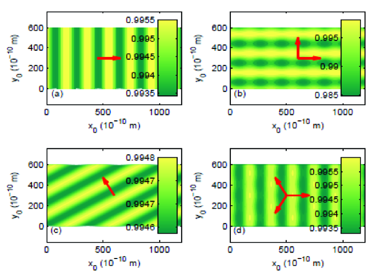
We consider four types of HM/SL patterns depicted in Fig. 2. Numerical results of the spin-up conductance are shown in Fig. 3. The spin-down conductance demonstrates similar pattern with different absolute values. In the contour as a function of the HM/SL layer center, it could be seen that the conductance significantly reproduce the HM/SL spin configurations with the lattice pattern and symmetry clearly recognizable. The absolute values of the spin-up conductance are close to 1 in unit of due to the static shallow well potential meV used and the pattern resemblance could be most prominently demonstrated. For the three- triangular SL, the C2-symmetric rectangular WG squeezes the C3-symmetric triangular lattice at the four sides giving rise to the reshaping of the unit lattice cell in the conductance. The triangular unit cell in the SL spin texture (see Fig. 2) is reshaped into an olive, which also occurs in the total skyrmion number depicted in Fig. 4 and later discussed. We consider the incident electron energy in between the first and second eigenlevels of the WG. The propagating and evanescent modes coherently contribute to the transmission. The third eigenlevel is far above the incident energy and the two levels considered, whose affect can be neglected. This is also justified by normalization of the scattering matrix taking into account the first and second eigenlevels. Work done by the two modes shares some similarity with taking a holographic picture. With single-mode incidence, the eigenlevel of the WG and that of the HM/SL scatterer do not coincide. The HM/SL is complete opaque therefore the conductance is absolute zero. When the evanescent mode enters the transmission, electron transport by two quantum paths interferes. One is direct transport by the propagating level, the other is through scattering to the evanescent mode at the HM/SL scatterer and then back to the propagating level. During interaction with the HM/SL scatter, the spin texture is imprinted in the second path. As evanescent mode cannot transport far, only by interfering with the first path, the spin texture information is recorded. Therefore, the conductance demonstrates a significant resemblance to the HM/SL spin pattern.
Results of the conductance could also be interpreted by the total skyrmion number for the SL case. Contour of the total skyrmion number defined in Eq. (8) as a function of the SL layer center coordinates is shown in Fig. 4. The integrand of equation (8) defines a topological magnetic field that gives rise to a Lorentz force and the total skyrmion number is proportional to the accumulated Berry phase in real space of travelling electrons within the total SL layer confined in the WGSL14 . A complete skyrmion vortex confined within the WG contribute a full single skyrmion number to the total skyrmion number. A partial skyrmion vortex confined within the WG contribute a partial skyrmion number depending on the radius of the confined area. For the three- triangular SL, the triagular unit lattice cell of the spin texture is reshaped into an olive in the total skyrmion number pattern due to symmetry compromise, which also occurs in the conductance. As an electron is scattered by the SL quantum well, it feels the Lorentz force of the topological magnetic feel. As the SL spin vortex whirls in the - plane, the topological magnetic field is in the direction. The effect of the Lorentz force generated by the magnetic field is to distort wavefunction in the - plane without changing the transport direction. As the distorted and undistorted wavefunction coming from the two quantum paths interferes, the SL spin texture is recorded. Similar to the SL, the HM has finite topological magnetic field with zero accumulated Berry phase. The wavefunction distortion and path interference occur as well. The conductance records the HM spin pattern as well.
To theoretically explain the experimental observed SL pattern, relative spatial shifts of helices were introducedSL1 to the spin vector field Eq. (4). This shift could broaden the skyrmion area and narrow the antiskyrmion area and give rise to identical spin pattern to the experiment. However, in our approach inclusion of the spatial shift of the helices frustrates the analytical solution of in our theory. In the Supplementary Section S1, we redid our theoretical treatment with phenomenological SL fields close to the experiment pattern. Characteristic periodic curves of the conductance as a function of the SL layer center coordinates are obtained hence the main findings can be reproduced.
IV Conclusions
The HM and SL have topologically nontrivial spin texture. The HM and SL can be together generalized into the multi- description with the HM a single- state, the square SL a double- state, and the triangular SL a triple- state. We theoretically proposed the device of HM/SL thin film embedded electron WG to investigate the relation between transport properties and the HM/SL spin texture. It is found that by translation of the embedded layer the conductance contour as a function of the HM/SL layer position significantly resemble that of the real-space contour of spin- component of the HM/SL spin vector field, which has one-to-one correspondence to a particular HM/SL spin configuration. When an electron transports in the WG through the HM/SL scatterer, the two quantum paths, i.e., the propagating mode and through the evanescent mode, interfere. When the electron interacts with the HM/SL scatterer through the second path, the topological magnetic field generalized by the HM/SL spin texture exerts on it and distorts the wavefunction shape in the - plane. By interference of the two paths, the HM/SL spin texture is recorded in the conductance. The contour pattern of the total skyrmion number as a function of the SL layer center position shares similar pattern with the conductance, which further consolidates the mechanism interpretation.
V Acknowledgements
The author acknowledges enlightening discussions with Wen-Ji Deng, Zhi-Lin Hou, and Li Zhang. This project was supported by the National Natural Science Foundation of China (No. 11004063) and the Fundamental Research Funds for the Central Universities, SCUT (No. 2014ZG0044).
References
- (1) J. I. Kishine and A. S. Ovchinnikov, Phys. Rev. B 79, 220405(R) (2009).
- (2) S. Mühlbauer, B. Binz, F. Jonietz, C. Pfleiderer, A. Rosch, A. Neubauer, R. Georgii, and P. Böni, Science 323, 915 (2009).
- (3) S. Seki, X. Z. Yu, S. Ishiwata, and Y. Tokura, Science 336, 198 (2012).
- (4) W. Münzer, A. Neubauer, T. Adams, S. Mühlbauer, C. Franz, F. Jonietz, R. Georgii, P. Böni, B. Pedersen, M. Schmidt, A. Rosch, and C. Pfleiderer, Phys. Rev. B 81, 041203 (2010).
- (5) S. Heinze, K. V. Bergmann, M. Menzel, J. Brede, A. Kubetzka, R. Wiesendanger, G. Bihlmayer, and S. Blügel, Nat. Phys. 7, 713 (2011).
- (6) T. Okubo, S. Chung, and H. Kawamura, Phys. Rev. Lett. 108, 017206 (2012).
- (7) D. L. Kovrizhin, Benoît Douçot, and R. Moessner, Phys. Rev. Lett. 110, 186802 (2013).
- (8) A. Neubauer, C. Pfleiderer, B. Binz, A. Rosch, R. Ritz, P. G. Niklowitz, and P. Böni, Phys. Rev. Lett. 102, 186602 (2009).
- (9) T. Schulz, R. Ritz, A. Bauer, M. Halder, M. Wagner, C. Franz, C. Pfleiderer, K. Everschor, M. Garst, and A. Rosch, Nat. Phys. 8, 301 (2012).
- (10) A. Manchon, N. Ryzhanova, A. Vedyayev, and B. Dieny, J. Appl. Phys. 103, 07A721 (2008);
- (11) R. Zhu, arXiv:1204.6095.
- (12) J. Heurich, J. König, and A. H. MacDonald, Phys. Rev. B 68, 064406 (2003).
- (13) C. Jia and J. Berakdar, Appl. Phys. Lett. 95, 012105 (2009).
- (14) C. Jia and J. Berakdar, Phys. Rev. B 81, 052406 (2010).
- (15) R. Zhu, J. Phys.: Condens. Matter 25, 036001 (2013).
- (16) R. Zhu and L.-J. Cui, Phys. Lett. A (in publish; Arxiv: 1310.6793).
- (17) F. Jonietz, S. Mühlbauer, C. Pfleiderer, A. Neubauer, W. Münzer, A. Bauer, T. Adams, R. Georgii, P. Böni, R. A. Duine, K. Everschor, M. Garst, and A. Rosch, Science 330, 1648 (2010).
- (18) E. Tekman and P. F. Bagwell, Phys. Rev. B 48, 2553 (1993).
- (19) D. Boese, M. Lischka, and L. E. Reichl, Phys. Rev. B 61, 5632 (2000).
- (20) R. A. Vicencio, A. V. Gorbach, and S. Flach, Phys. Lett. A 354, 210 (2006).
- (21) F. N. Rybakov, A. B. Borisov, and A. N. Bogdanov, Phys. Rev. B 87, 094424 (2013).