A planar hyperlens based on a modulated graphene monolayer
Abstract
The canalization of terahertz surface plasmon polaritons using a modulated graphene monolayer is investigated for subwavelength imaging. An anisotropic surface conductivity formed by a set of parallel nanoribbons with alternating positive and negative imaginary conductivities is used to realize the canalization regime required for hyperlensing. The ribbons are narrow compared to the wavelength, and are created electronically by gating a graphene layer over a corrugated ground plane. Good quality canalization of surface plasmon polaritons is shown in the terahertz even in the presence of realistic loss in graphene, with relevant implications for subwavelength imaging applications.
keywords:
surface plasmon polariton, graphene, canalization, sub-wavelength imagingDepartment of Electrical Engineering, University of Wisconsin-Milwaukee, 3200 N. Cramer St., Milwaukee, Wisconsin 53211, USA]University of Wisconsin-Milwaukee Center for Applied Electromagnetic Systems Research (CAESR), Department of Electrical Engineering, University of Mississippi, University, Mississippi 38677-1848, USA]University of Mississippi Department of Electrical and Computer Engineering, University of Texas at Austin, Austin, Texas 78712, USA]The University of Texas at Austin \abbreviationsSPP,THz
1 ========================
Graphene, the first 2D material to be practically realized1, has attracted great interest in the last decade. The fact that electrons in graphene behave as massless Dirac-Fermions leads to a variety of anomalous properties 2, 3, such as charge carriers with ultra high-mobility and long mean-free paths, gate-tunable carrier densities, and anomalous quantum Hall effects 4. Graphene’s electrical properties have been studied in many previous works 5, 6, 7, 8, 9, 10, 11, 12, 13, 14 and are often represented by a local complex surface conductivity given by the Kubo formula 15, 16. Since its surface conductivity leads to attractive surface plasmon properties, graphene has become a good candidate for plasmonic applications, especially in the terahertz (THz) regime 17, 18, 19, 20, 21, 22, 23.
Surface plasmons (SPs) are the collective charge oscillations at the surface of plasmonic materials. SPs coupled with photons form the composite quasi-particles known as surface plasmon polaritons (SPPs). Theoretically, the dispersion relationship for SPPs on a surface can be obtained as a solution of Maxwell’s equations 24. In this approach it is easy to show that, in order to support the SPP, 3D materials with negative bulk permittivities ( noble metals) or 2D materials with non-zero imaginary surface conductivities ( graphene) are essential. Although SPPs on metals and on graphene have considerable qualitative similarities, graphene SPPs generally exhibit stronger confinement to the surface, efficient wave localization up to mid-infrared frequencies 25, 19, and they are highly tunable (which is one of their most unique and important properties)3. Applications of graphene SPPs include electronics 26, 27, 28, optics 29, 30, 31, THz technology 32, 33, 34, light harvesting 35, metamaterials 36, and medical sciences 37, 38.
In this work we study the canalization of SPPs on graphene, which can have direct applications for sub-wavelength imaging using THz sources.
Sub-wavelength imaging using metamaterials was first reported by Pendry in 2000 39. His technique 40 was based on backward waves, negative refraction and amplification of evanescent waves. More recently, another more robust venue for subwavelength imaging was proposed, based on metamaterials operating in the so called “canalization regime” 41, 42, 43. In this case, the structure (acting as a transmission medium) transfers sub-wavelength images from a source plane to an image plane over distances of several wavelengths, without diffraction 44. This form of super-resolving imaging, or hyperlensing, can also be realized by a uniaxial wire medium 45. In these schemes, all spatial harmonics (evanescent and propagating) propagate with the same phase velocity from the near- to the far-field. In this paper we discuss the canalization of SPPs on a modulated graphene monolayer. In Ref. 46, it was shown that the near field of a vertical point source placed in close proximity to a graphene monolayer couples primarily to the field of an SPP strongly confined to the monolayer. By creating an anisotropic graphene surface as alternating graphene nanoribbons with positive and negative imaginary surface conductivities, we achieve SPP canalization and hyperlensing of the near-field of an arbitrary source.
To achieve canalization, it is necessary to realize a flat isofrequency contour47. Here, taking the same definition for canalization as for a 3D material, we first study the conditions for canalization of SPPs on a 2D material such as graphene. Then, a practical geometry is proposed and verified for the hyperlens implementation.
2 Theory and results
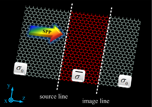
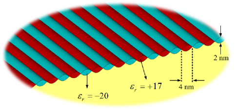
Figure 1 shows an infinite graphene layer in the plane suspended in vacuum. Its surface conductivity is assumed isotropic () everywhere except in the region between the source and image lines (red colored region), which is anisotropic and is given as
| (1) |
where for now are assumed to be imaginary-valued, (to be generalized later) . For an SPP traveling over such an anisotropic graphene layer, it is possible [see Supporting Information (SI)] to show that the governing dispersion relation is
| (2) |
where is the wavenumber in free space, is the intrinsic impedance of vacuum, , and the 2D spatial Fourier transform variables are .
From (2), an ideal canalization regime can be realized when
| (3) |
simultaneously, such that (2) becomes
| (4) |
independent of . Equation (4) implies that all of the transverse spatial harmonics ( of the SPPs) will propagate with the same wavenumber (phase velocity) in the -direction. In this situation, which is analogous to the canalization regime in 3D metamaterials, any SPP distribution at the source line in Fig. 1 will be transferred to the image line without diffraction or any phase distortion. Condition (3) is somewhat analogous to the condition required for canalization of 3D waves in Ref. 48, but with the difference that here the extreme parameters (3) yield a finite wave number, equal to the background medium surrounding the modulated graphene layer, and not zero as for the 3D case. This is to be expected, since the canalized SPPs still need to be above the light cone to avoid radiation and leakage in the background medium. Quite peculiarly, it follows from (4) that the confinement in the transverse () direction of each SPP is proportional to its spatial frequency along , i.e., .
It might seem difficult to find a natural 2D material providing (3) for canalization. However, it can be shown [see SI] that a modulated isotropic conductivity can act as an effective anisotropic conductivity,
| (5) |
| (6) |
where is assumed to be periodic with period , and the integrations are over one period. Note that should be small compared to the wavelength in order to provide valid effective parameters. Therefore, if the isotropic conductivity of graphene is properly modulated ( by electrical gating or chemical doping), its effective anisotropic conductivity can indeed satisfy (3).
In the following, two conductivity modulations will be analyzed whose effective anisotropic conductivities satisfy (3) and are thus in principle capable of canalizing SPPs. Since we will use full-wave simulations to confirm the canalization geometries, a section in the SI is dedicated to modeling of graphene in commercial simulation codes using finite-thickness dielectrics.
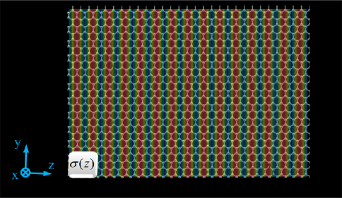
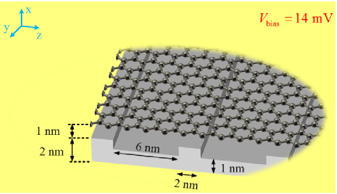
2.1 Modulated conductivity using ridged ground planes
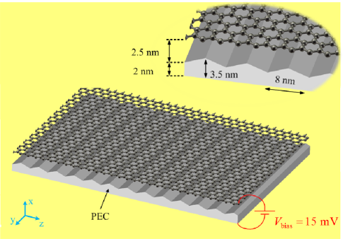
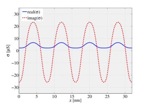
In previous canalization metamaterials, or hyperlenses, using alternating positive and negative dielectrics, an idealized, abrupt transition has been assumed between layers. For graphene, this would be analogous to strips having abrupt transitions between positive and negative imaginary-part conductivities. We refer to this as the hard-boundary case, and analyze it in detail in the SI. However, given the finite quantum capacitance of graphene, such an abrupt transition is impossible to achieve. A more realistic modulation scenario for a conductivity profile satisfying (3) can be obtained in the geometry of Fig. 2. It consists of an infinite sheet of graphene gated by a ridged ground plane, as shown in the insert of Fig. 2. Performing a static analysis, it is possible to obtain the charge density on the graphene layer, which may in turn provide the chemical potential and the conductivity of graphene following a method analogous to Ref. 23. Figure 3 shows the calculated conductivity of the graphene layer as a function of (using the complex conductivity predicted by the Kubo formula; see Ref. 11 for the explicit expression for , , ).
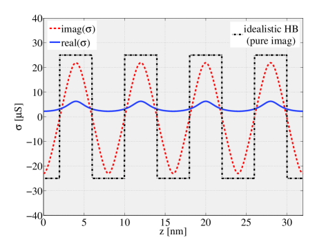
Two important conclusions can be drawn from Fig. 3: i) the imaginary part of conductivity dominates the real part, as desired, and ii) its distribution is almost perfectly sinusoidal, which, after insertion into (5) and (6), satisfies (3). Therefore, the geometry of Fig. 2 may be expected to support canalization. The resulting graphene nanoribbons have a realistic smooth variation in conductivity; we refer to this geometry as the soft-boundary scenario, considered in the following.
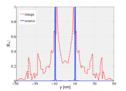
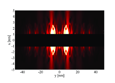
As an example, two point sources are placed in front of the source line in Fig. 1, exciting SPPs on the graphene layer. The point sources are separated by nm, where nm using (S.2) in the Supporting Information, and the canalization area (the region between the source and the image lines) has length nm and width of 100 nm (which is large compared to the separation between sources).
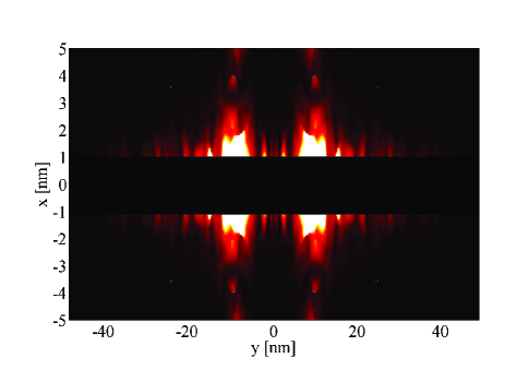
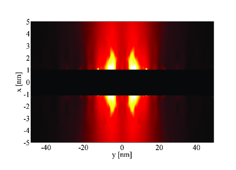
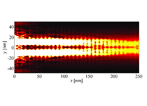
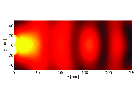
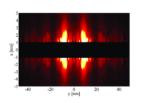
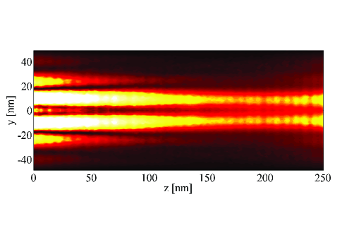
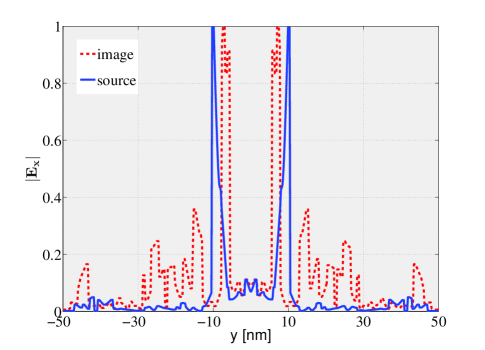
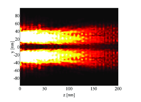
Figure 4 shows the -component of the electric field at the source line and image line (at the end of the modulated region). The plot of the normalized -component of the field at nm is shown in Fig. 5, while Figure 6 shows the -component of the electric field above the modulated graphene surface, and a homogenous graphene surface with conductivity S. This shows quite strikingly how the canalization occuring on the modulated graphene can avoid the usual diffraction expected on a homogeneous layer. Figs. S.3-S.5 in the SI show consistent results for the hard-boundary case.
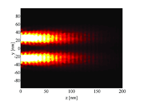
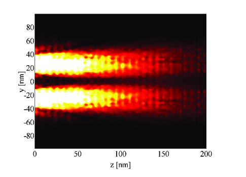
It is easy to show that (5) and (6) cannot be exactly satisfied if the conductivity includes loss (i.e., the real part of ). Therefore as loss increases, the phase velocities will differ among various spatial components and, as a result, one would expect to see a blurred image, and eventually no image, as loss further increases. To investigate this deterioration effect, we decrease the canalization length to nm and increase the separation between sources to nm (which we found necessary to maintain accuracy in the simulation). The geometry is then simulated for soft- and hard-boundary cases (with and without loss for each case) and the - components of the electric field at nm are shown in Fig. 7. The curves are calculated in the image line at a distance nm above the graphene surface.
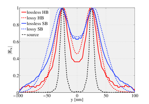
Comparison between the four curves in Fig. 7 shows that the lossless hard- and soft-boundary examples yield similar results, as expected since their effective surface conductivity satisfies (3) exactly. In fact, as long as the period is small compared to the wavelength, any modulation which has half-wave symmetry will satisfy (3), leading to perfect canalization.
However, adding loss causes the effective surface conductivities to have non-vanishing real parts, and therefore (3) cannot be exactly satisfied. In the lossy case, the modulation scheme is important, since it affects how closely (3) can be satisfied. For example, Fig. 7 shows that the idealistic hard-boundary model exhibits better resolution than the realistic soft-boundary model.
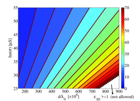
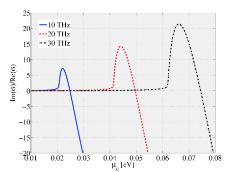
Image degradation due to loss can be lessened by working at higher frequencies. In fact, the maximum of the ratio Im()/Re() may be increased by adjusting the chemical potential at higher frequencies. In the SI the ratio Im()/Re() is plotted as a function of chemical potential and frequency, and its optimal value for three different frequencies is used to simulate to the same geometry. The simulation results confirm the improvement of canalization as frequency increases.
Our results show that a triangular ridged ground plane to bias the graphene monolayer indeed allows canalization and hyperlensing, since its effective conductivities given by (5) and (6) satisfy (3). However, there are many possible functions that, after inserting them into (5) and (6), will satisfy (3). As an example, the sinusoidal conductivity of Fig. 3 can also be implemented using a rectangular ridged ground plane (details are shown in the SI).
3 Conclusions and future scope
We have analyzed the possibility to produce in-plane canalization of SPPs on a 2D surface, with particular emphasis on its realization in a realistically modulated graphene monolayer, resulting in a planarized 2D hyperlens on graphene. We envision the use of this effect on a ridged ground plane for sub-wavelength imaging of THz sources and to arbitrarily tailor the front wave of an SPP by suitably designing the boundary of the canalization region.
4 Methods
Simulations were performed with CST Microwave Studio 49 using a dielectric slab model of graphene, with the conductivity coming from the Kubo formula 15, 16. The Supplemental Information describes in detail the model, contains proofs of various equations appearing in the text, and presents additional results.
5 Supporting Information
5.1 On the modeling of graphene layer by a thin dielectric
Modeling graphene as a 2D surface having an appropriate value of surface conductivity is an accurate approach for a semiclassical analysis (e.g., the Drude model for intraband contributions has been verified experimentally 50, 51, 52, and the interband model and the visible-spectrum response have also been verified 52). However, often it is convenient to model graphene as a thin dielectric layer, which is easily implemented in typical electromagnetic simulation codes. It is common to consider an equivalent dielectric slab with the thickness of and a 3D conductivity of . The corresponding bulk (3D) relative permittivity is 17
| (S.7) |
where is the angular frequency. However, for calculations in which the geometry is discretized (e.g., in the finite-element method), fine features in the geometry such as an electrically-thin slab demand finer discretization, which in turn requires more computational costs. Thus, whereas sub thickness values may seem more physically-appropriate, numerical considerations often lead to the use of a thicker material. As an example, in Ref. 17 the thickness of the dielectric slab is assumed to be .
However, the accuracy of the dielectric model degrades as the thickness of the slab increases. Since this model is widely adopted, yet a detailed consideration of this effect has not been previously presented, we briefly consider this topic below.
Consider a transverse magnetic SPP on an infinite graphene layer. The SPP wavelength using the 2D conductivity is 11
| (S.8) |
where is the wavelength in free space. On the other hand, in Ref. 53 it is shown that a dielectric slab with negative permittivity ambient in a medium with positive permittivity can support two sets of dielectric modes (even and odd). The odd modes have the wavelength (assuming vacuum as the ambient medium)
| (S.9) |
where and are the dielectric slab permittivity and thickness, respectively. It is shown in Ref. 53 that the odd modes can exist only if
| (S.10) |
It can also be noticed that the modal field distribution outside of the slab is similar to that of a SPP on graphene. It is easy to show that in the limit of and using (S.7), the dielectric-slab odd mode becomes the graphene SPP mode . It can be shown that (S.9) is a good approximation for only if three conditions are satisfied as [see the next sub-section]
| (S.11) |
| (S.12) |
| (S.13) |
Equation (S.13) is in fact the direct insertion of (S.7) into (S.10). Based on (S.13), as the ratio increases, the dielectric slab becomes a better approximation (as long as (S.12) is not violated). To consider this, Fig. S.8 shows the frequency independent error (%) of using the dielectric slab model for graphene as a function of the normalized and (assuming is imaginary-valued),
| (S.14) |
As a numerical example (using equations (3) and (4) in Ref. 11), for nm, the scattering rate , and chemical potential at and very low temperature (), the normalized thickness and conductivity will be and S which leads to an error of . This is set as the maximum error that is allowed in the rest of this work.
5.2 Proof of (S.13)
From (S.9),
| (S.15) |
where and .
Assuming , (S.15) leads to
| (S.16) |
After keeping only the first term of the series in (S.16) and using the assumption ,
| (S.17) |
| (S.18) |
5.3 Proof of (2)
For the anisotropic region of Fig. 1, consider a general magnetic field in the Fourier transform domain as
| (S.19) |
where are constants. Equation (S.19) is chosen so that it satisfies the Helmholtz equation and has the form of a plasmonic wave.
Using Ampere’s law to find the electric field in each region and satisfying the boundary conditions
| (S.20) |
| (S.21) |
| (S.22) |
it is straightforward to show that
| (S.23) |
| (S.24) |
| (S.25) |
where , and Setting the determinant of the above matrix to zero leads to (2).
It is easy to show that in the isotropic limit (), (2) simplifies to the well-known dispersion equations 7, 11 , and , for transverse magnetic (TM) and transverse electric (TE) surface waves, respectively. The solution of (2) will lead to a solution for the SPP with the magnetic field
| (S.26) |
In the canalization regime, the SPP given by (S.26) is a TM mode with respect to the canalization direction (-direction in our notation) and its magnetic field has a peculiar circular polarization,
| (S.27) |
It is also interesting that the confinement in the -direction of each SPP harmonic is proportional to .
5.4 Proof of (5) and (6)
Assume a sheet of graphene with a periodic isotropic conductivity in the -direction () as shown in Fig. S.9. Enforcing a constant, uniform, and -directed surface current on the graphene induces an electric field on the graphene as
| (S.28) |
Defining average parameters leads to
| (S.29) |
| (S.30) |
Enforcing a constant, uniform and -directed electric field () induces a surface current on the graphene as
| (S.31) |
which is (5).
Defining average parameters leads to
| (S.32) |
| (S.33) |
which is (6).
5.5 Idealized graphene nanoribbons with hard-boundaries
An idealization of the modulation scheme discussed in the text would consist of alternating positive and negative imaginary conductivities, with each strip terminating in a sharp transition between positive and negative values (see Fig. S.13). We assume that all of the strips have the same width nm and conductivity modulus S, which is the conductivity of a graphene layer for , , and or (for positive and negative , respectively). The chemical potential is chosen to minimize the loss at the given frequency. In fact, the ratio is maximized at this frequency (the ratio is 7 for eV). Since the effect of loss was discussed in the text, here we assume an imaginary-valued conductivity S.
We refer to this idealized conductivity profile as the hard-boundary case, because of the step discontinuity (sharp transition) of the conductivity between neighboring strips. This resembles the geometry in Ref. 48 for canalization of 3D waves in which there are also hard-boundaries between dielectric slabs with positive and negative permittivites.
As a simulation example of the hard-boundary case, two point sources are placed in front of the source line in Fig. 1 exciting two SPPs on the graphene layer. The point sources are separated by nm where nm using (S.8), and the canalization area (the region between the source and the image lines) has length nm and width of 100 nm (which is large compared to the separation between sources). Figure S.10 shows the normalized -component of the electric field at the source line and image line (at the end of the modulated region). Fig. S.11 shows the normalized -component of the electric field above the surface of the graphene (nm). Note that the region nm represents the graphene (since we have used a dielectric slab model for graphene with the thickness of nm).
5.6 Simulation setup for the hard- and the soft-boundary examples
Full-wave simulations have been done using CST Microwave Studio 49. In this section we consider the dielectric model of graphene. Figure S.13 shows the simulation setup of the hard-boundary example. The simulation results are given in Figs. S.10-S.12. The graphene strips can be modeled with dielectric slabs having thickness nm and, using (S.7), permittivities of and . However, as shown in the insert of Fig. S.13, the permittivity is used rather than because numerical experiments show that that value leads to better canalization. The difference with our analytically-predicted value for best canalization is seemingly because in our analytical model we have disregarded radiation, reflections from discontinuities, and similar effects.
For the soft-boundary example, the conductivity of the strips varies smoothly with position. So, applying the dielectric slab model, we could use a dielectric slab with a fixed thickness (e.g., nm) and a position dependent permittivity given by (S.7) as
| (S.34) |
However, an alternative method which is easier to implement for simulation is to consider a dielectric slab with fixed permittivity (or permittivities) and a position dependent thickness as
| (S.35) |
Obviously, two different values should be chosen for different signs of so that remains positive. This has been done for the conductivity of Fig. 3, and the resulting dielectric slab model is shown in Fig. S.14. Comparison between Fig. S.13 and Fig. S.14 clearly shows the difference between the hard- and the soft-boundary examples.
5.7 The improvement of canalization by increasing the frequency
Figure S.15 shows the ratio Im()/Re() versus chemical potential at three different frequencies, showing that, as frequency increases, loss becomes less important. Note also that the value of chemical potential that maximizes the conductivity ratio is considerably frequency dependent. In Fig. S.16 the effect of decreasing loss as a result of the frequency increase is invesigated. To do so, the peak ratio Im()/Re() of the three curves in Fig. S.15 are chosen associated with frequencies 10, 20, and 30 THz. These ratios are assigned to a same geometry (and holding frequency constant) and the -component of the electric fields are shown in Fig. S.16 (the scalings are the same). In this way, all of the electrical lengths (such as the electrical length of the nanoribbons, canalization region, etc.) remain the same and only the effect of loss is incorporated. From Fig. S.16, it is obvious that the increase of frequency improves the canalization. However, since the dimensions become smaller, fabrication becomes more difficult.
5.8 Modulated graphene conductivity using a rectangular ridged ground plane
The sinusoidal conductivity of Fig. 3 can be implemented using a rectangular ridged ground plane, as shown in Fig. S.17. The conductivity distribution of the geometry in Fig. S.17 is shown in Fig. S.18 and is almost identical to Fig. 3, although their ground plane geometries are different. Obviously, the ideal canalization behavior of the two geometries is very similar. Interestingly, the rectangular ridged ground plane has to be non-symmetric (the ratio of groove to ridge is 3) to produce the same conductivity function as the symmetrical triangular ridged ground plane.
References
- Novoselov et al. 2004 Novoselov, K. S.; Geim, A. K.; Morozov, S. V.; Jiang, D.; Zhang, Y.; Dubonos, S. V.; Grigorieva, I. V.; Firsov, A. A. Electric Field Effect in Atomically Thin Carbon Films. Science 2004, 306, 666–669
- Castro Neto et al. 2009 Castro Neto, A. H.; Guinea, F.; Peres, N. M. R.; Novoselov, K. S.; Geim, A. K. The Electronic Properties of Graphene. Rev. Mod. Phys. 2009, 81, 109–162
- Luo et al. 2013 Luo, X.; Qiu, T.; Lu, W.; Ni, Z. Plasmons in Graphene: Recent Progress and Applications. Materials Science and Engineering: R: Reports 2013, xx, xxx
- Zhang et al. 2005 Zhang, Y.; Tan, Y. W.; Stormer, H. L.; Kim, P. Experimental Observation of the Quantum Hall Effect and Berry’s Phase in Graphene. Nature 2005, 438, 201–204
- Falkovsky and Varlamov 2007 Falkovsky, L. A.; Varlamov, A. A. Space-Time Dispersion of Graphene Conductivity. Eur. Phys. J. B 2007, 56, 281–284
- Falkovsky and Pershoguba 2007 Falkovsky, L. A.; Pershoguba, S. S. Optical Far-Infrared Properties of a Graphene Monolayer and Multilayer. Phys. Rev. B 2007, 76, 153410
- Mikhailov and Ziegler 2007 Mikhailov, S. A.; Ziegler, K. New Electromagnetic Mode in Graphene. Phys. Rev. Lett. 2007, 99, 016803
- Gusynin and Sharapov 2006 Gusynin, P.; Sharapov, S. G. Transport of Dirac Quasiparticles in Graphene: Hall and Optical Conductivities. Phys. Rev. B 2006, 73, 245411
- Gusynin et al. 2006 Gusynin, V. P.; Sharapov, S. G.; Carbotte, J. P. Unusual Microwave Response of Dirac Quasiparticles in Graphene. Phys. Rev. Lett. 2006, 96, 256802
- Peres et al. 2006 Peres, N. M. R.; Neto, A. C.; Guinea, F. Conductance Quantization in Mesoscopic Graphene. Phys. Rev. B 2006, 73, 195411
- Hanson 2008 Hanson, G. W. Dyadic Greens Functions and Guided Surface Waves for a Surface Conductivity Model of Graphene. J. Appl. Phys. 2008, 103, 064302
- Hanson 2008 Hanson, G. W. Dyadic Green’s Functions for an Anisotropic, Non-Local Model of Biased Graphene. IEEE Trans. Antennas Propagat. 2008, 56, 747–757
- Peres et al. 2006 Peres, N. M. R.; Guinea, F.; Neto, A. C. Electronic Properties of Disordered Two-Dimensional Carbon. Phys. Rev. B 2006, 73, 125411
- Ziegler 2007 Ziegler, K. Minimal Conductivity of Graphene: Nonuniversal Values from the Kubo Formula. Phys. Rev. B 2007, 75, 233407
- Ashcroft and Mermin 1976 Ashcroft, N.; Mermin, N. Solid State Physics; Saunders College, 1976
- Gusynin et al. 2007 Gusynin, V. P.; Sharapov, S. G.; Carbotte, J. P. Magneto-Optical Conductivity in Graphene. J. Phys.: Condens. Matter 2007, 19.2, 026222
- Vakil and Engheta 2011 Vakil, A.; Engheta, N. Transformation Optics Using Graphene. Science 2011, 332.6035, 1291–1294
- Christensen et al. 2011 Christensen, J.; Manjavacas, A.; Thongrattanasiri, S.; Koppens, F. H. L.; de Abajo, F. J. G. Graphene Plasmon Waveguiding and Hybridization in Individual and Paired Nanoribbons. Phys. Rev. B 2011, 86, 235440
- Hanson et al. 2012 Hanson, G. W.; Forati, E.; Linz, W.; Yakovlev, A. B. Excitation of THz Surface Plasmons on Graphene Surfaces by an Elementary Dipole and Quantum Emitter: Strong Electrodynamic Effect of Dielectric Support. Phys. Rev. B 2012, 86, 235440 (1–9)
- Nikitin et al. 2011 Nikitin, A. Y.; Guinea, F.; Garcia-Vidal, F. J.; Martin-Moreno, L. Edge and Waveguide THz Surface Plasmon Modes in Graphene Micro-Ribbons. arXiv 2011, 1107.5787
- Sounas and Caloz 2011 Sounas, D. L.; Caloz, C. Edge Surface Modes in Magnetically Biased Chemically Doped Graphene Strips. Appl. Phys. Lett. 2011, 98, 021911
- Wang et al. 2011 Wang, W.; Apell, P.; Kinaret, J. Edge Plasmons in Graphene Nanostructures. Phys. Rev. B 2011, 84, 085423
- Forati and Hanson 2013 Forati, E.; Hanson, G. W. Surface Plasmon Polaritons on Soft-Boundary Graphene Nanoribbons and Their Application in Switching/Demultiplexing. Appl. Phys. Lett. 2013, 103, 133104
- Raether 1988 Raether, H. Surface Plasmons; Springer: Berlin, 1988
- Nikitin et al. 2011 Nikitin, A. Y.; Guinea, F.; Garcia-Vidal, F. J.; Martin-Moreno, L. Fields Radiated by a Nanoemitter in a Graphene Sheet. Phy. Rev. B 2011, 84, 195446
- Berger et al. 2006 Berger, C.; Song, Z.; Li, X.; Wu, X.; Brown, N.; Naud, C.; Mayou, D.; Li, T.; Hass, J.; Marchenkov, A. N. Electronic Confinement and Coherence in Patterned Epitaxial Graphene. Science 2006, 312, 1191–1196
- Mueller et al. 2009 Mueller, T.; Xia, F.; Freitag, M.; Tsang, J.; Avouris, P. Role of Contacts in Graphene Transistors: A Scanning Photocurrent Study. Phys. Rev. B 2009, 79, 245430
- Nair et al. 2008 Nair, R. R.; Blake, P.; Grigorenko, A. N.; Novoselov, K. S.; Booth, T. J.; Stauber, T.; Peres, N. M. R.; Geim, A. K. Fine Structure Constant Defines Visual Transparency of Graphene. Science 2008, 320, 1308
- Bonaccorso et al. 2010 Bonaccorso, F.; Sun, Z.; Hasan, T.; Ferrari, A. C. Graphene Photonics and Optoelectronics. Nat. Photon. 2010, 4, 611–622
- Xia et al. 2009 Xia, F. N.; Mueller, T.; Lin, Y. M.; Valdes-Garcia, A.; Avouris, P. Ultrafast Graphene Photodetector. Nat. Nanotechnol. 2009, 4, 839–843
- Mak et al. 2008 Mak, K. F.; Sfeir, M. Y.; Wu, Y.; Lui, C. H.; Misewich, J. A.; Heinz, T. F. Measurement of the Optical Conductivity of Graphene. Phys. Rev. Lett. 2008, 101, 196405
- Otsuji et al. 2012 Otsuji, T.; Tombet, S. B.; Satou, A.; Fukidome, H.; Suemitsu, M.; Sano, E.; Popov, V.; Ryzhii, M.; Ryzhii, V. Graphene-Based Devices in Terahertz Science and Technology. J. Phys. D: Appl. Phys. 2012, 45, 303001
- Docherty and Johnston 2012 Docherty, C.; Johnston, M. Terahertz Properties of Graphene. J. Infrared Millim. Terahertz Waves 2012, 33, 797–815
- G mez-D az et al. 2013 G mez-D az, J. S.; Esquius-Morote, M.; Perruisseau-Carrier, J. Plane Wave Excitation-Detection of Non-Resonant Plasmons Along Finite-Width Graphene Strips. Optics Express 2013, 21, 24856–24872
- Jiang et al. 2012 Jiang, Y.; Lu, W.; Xu, H.; Dong, Z.; Cui, T. A Planar Electromagnetic Black Hole Based on Graphene. Phy. Lett. A 2012, 376, 1468–1471
- Chen and Alù 2011 Chen, P. Y.; Alù, A. Atomically Thin Surface Cloak Using Graphene Monolayers. ACS Nano 2011, 5, 5855–5863
- Liu et al. 2012 Liu, Y.; Dong, X.; Chen, P. Biological and Chemical Sensors Based on Graphene Materials. Chem. Soc. Rev. 2012, 41, 2283–2307
- Szunerits et al. 2013 Szunerits, S.; Maalouli, N.; Wijaya, E.; Vilcot, J.; Boukherroub, R. Recent Advances in the Development of Graphene-Based Surface Plasmon Resonance (SPR) Interfaces. Anal. Bioanal. Chem. 2013, 405, 1435–1443
- Pendry 2000 Pendry, J. B. Negative Refraction Makes a Perfect Lens. Phys. Rev. Lett. 2000, 85, 3966
- Veselago 1968 Veselago, V. The Electrodynamics of Substances with Simultanously Negative Values of and . Sov. Phys. Usp. 1968, 10, 509–514
- Ikonen et al. 2006 Ikonen, P.; Belov, P. A.; Simovski, C. R.; Maslovski, S. I. Experimental Demonstration of Subwavelength Field Channeling at Microwave Frequencies Using a Capacitively Loaded Wire Medium. Phys. Rev. B 2006, 73, 073102
- Narimanov and Shalaev 2007 Narimanov, E. E.; Shalaev, V. M. Optics: Beyond Diffraction. Nature 2007, 447.7142, 266–267
- Salandrino and Engheta 2006 Salandrino, A.; Engheta, N. Far-field Subdiffraction Optical Microscopy Using Metamaterial Crystals: Theory and Simulations. Phys. Rev. B 2006, 74, 075103
- Belov and Hao 2006 Belov, P. A.; Hao, Y. Subwavelength Imaging at Optical Frequencies Using a Transmission Device Formed by a Periodic Layered Metal-Dielectric Structure Operating in the Canalization Regime. Phys. Rev. B 2006, 73, 113110
- Belov et al. 2008 Belov, P. A.; Zhao, Y.; Tse, S.; Ikonen, P.; Silveirinha, M. G.; Simovski, C. R.; Tretyakov, S. Transmission of Images with Subwavelength Resolution to Distances of Several Wavelengths in the Microwave Range. Phy. Rev. B 2008, 77, 193108
- Hanson et al. 2011 Hanson, G. W.; Yakovlev, A. B.; Mafi, A. Excitation of Discrete and Continuous Spectrum for a Surface Conductivity Model of Graphene. J. Appl. Phys. 2011, 110, 114305
- Belov et al. 2005 Belov, P. A.; Simovski, C. R.; Ikonen, P. Canalization of Subwavelength Images by Electromagnetic Crystals. Phys. Rev. B 2005, 71, 193105
- Ramakrishna et al. 2003 Ramakrishna, S. A.; Pendry, J. B.; Wiltshire, M. C. K.; Stewartar, W. J. Imaging the Near Field. J. Mod. Opt. 2003, 50, 1419–1430
- 49 CST Microwave Studio, http://www.cst.com
- Li et al. 2008 Li, Z. Q.; Henriksen, E. A.; Jiang, Z.; Hao, Z.; Martin, M. C.; Kim, P.; Stormer, H. L.; Basov, D. N. Dirac Charge Dynamics in Graphene by Infrared Spectroscopy. Nat. Phys. 2008, 4, 532–535
- Kim et al. 2011 Kim, J. Y.; Lee, C.; Bae, S.; Kim, K. S.; Hong, B. H.; Choi, E. J. Far-Infrared Study of Substrate-Effect on Large Scale Graphene. Appl. Phys. Lett. 2011, 98, 201907
- Lee et al. 2011 Lee, C.; Kim, J. Y.; Bae, S.; Kim, K. S.; Hong, B. H.; Choi, E. J. Optical Response of Large Scale Single Layer Graphene. Appl. Phys. Lett. 2011, 98, 071905
- Alù and Engheta 2006 Alù, A.; Engheta, N. Optical Nanotransmission Lines: Synthesis of Planar Left-Handed Metamaterials in the Infrared and Visible Regimes. JOSA B 2006, 23, 571–583