Microscopic theory of tunneling spectroscopy in Sr2RuO4
Abstract
We study the surface Andreev bound state (ABS) of superconducting Sr2RuO4, which is a candidate material for the realization of the chiral -wave superconducting state. In order to clarify the role of chiral edge modes as ABSs, the surface density of states and the tunneling conductance is calculated in the normal metal/Sr2RuO4 junction within the framework of recursive Green’s function method, while taking into account the orbital degrees of freedom (including Spin-Orbit interactions) with realistic material parameters. In Sr2RuO4, there are two bands and originating from quasi-one-dimensional orbitals and and a two-dimensional band originating from orbital. We discuss about the contributions of various electronic bands to LDOS and the influence of atomic spin-orbit interaction (SOI). In the light of our calculations, quasi-one-dimensional model with dominant pair potentials in and bands is consistent with conductance measurements in Au/Sr2RuO4 junctions.
1 Introduction
Sr2RuO4 has attracted much interest for its unconventional superconductivity appearing at K.[1] There have been several experimental reports consistent with spin-triplet pairing [2, 3, 4, 5] with broken time reversal symmetry.[6] The most promising candidate for the pairing symmetry of the pair potential is the so-called spin-triplet chiral -wave state, whose pair potential can be represented as in the free electron model.[7] This state is the two-dimensional analog of the -phase of superfluid 3He, and can be categorized as topological superconductors.[8, 9] In topological superconductors, gapless Andreev bound states (ABSs) appear at their edges due to bulk-edge correspondence which are symmetrically protected by the bulk energy gap.[10, 11, 12, 13, 14] For the chiral -wave case, a gapless ABS with linear dispersion is generated.[15, 9] Although there have been several attempts to observe the chiral edge modes directly, their existence was not confirmed experimentally yet.[16, 17]
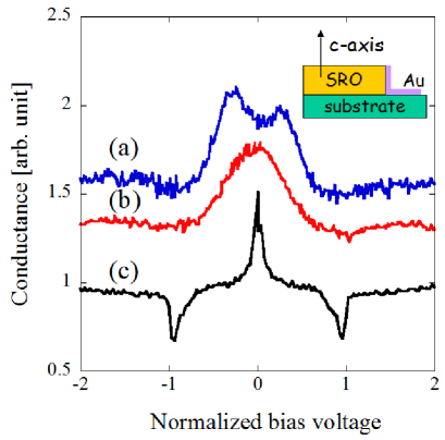
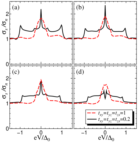
One of the few efficient ways to detect the chiral edge modes indirectly is tunneling conductance between normal metal/superconducting junctions.[18, 19] For example, a sharp zero-bias conductance peak (ZBCP) has been predicted in spin-singlet -wave superconductors by the ABS with flat dispersion.[20, 18] Due to this flat-band dispersion, ZBCP ubiquitously emerges in actual experiments in high cuprates. [21, 22, 23, 24, 25, 26, 27, 28] On the other hand, performing tunneling spectroscopy experiments in Sr2RuO4 junctions is not an easy task. Although Sr2RuO4 has extremely fragile surface, tunneling spectroscopy experiments have been performed on i) c-axis surface,[29, 30, 31, 32, 33] ii) in-plane,[34, 35] and iii) 3K-phase.[36, 37] As for c-axis tunneling, several reliable data are obtained using scanning tunneling microscopy/spectroscopy (STM/S) on in-situ cleaved surfaces. The most important feature observed in common is that conductance spectra exhibit gap feature except for zero-bias peak obtained at the vortex cores. The gap spectra show residual conductance at the zero-bias about 85 [29] and 50,[30] while a fully opened gap has been detected in the Al tip case.[32] The variety of gap amplitudes for three different bands obtained in the specific heat measurements [38] are not discernible for these experiments. In the case of ab-plane tunneling spectroscopy, due to the extreme difficulty in surface treatment, the number of experiments reported are quite limited. [34, 35] The data of point contact spectroscopy and thin film junction formed on cleaved surface in vacuum, shows the presence of the zero-bias conductance peaks in common, which suggest the formation of gapless ABS at the in-plane edges. Comparing with the zero-bias conductance peaks obtained in high- cuprates, the dome-like peak spreading in the whole gap amplitude observed on Sr2RuO4 indicates the formation of dispersive edge states expected for chiral -wave superconductors.[39, 40, 41] The shapes of the peak show variation depending on the junction (see Fig.1). Compared to the fragile 1.5K phase surfaces, the 3K phases of Sr2RuO4 tends to have stable surfaces due to the inclusion of inert surface of Ru. Conductance spectra obtained on these 3K phase commonly exhibit a sharp narrow peak near zero-bias in addition to the broad peak spreading in the whole gap amplitude [36, 37] (see curve (c) in Fig. 1). However, the origin of this two-step peak has not been clarified. One of the proposals for the superconducting state in 3K-phase is the inhomogeneous gap structure near the Ru-inclusions.[42] However, it is still an experimentally unresolved problem. Since two-step peaks in 1.5K-phase were recently observed by one of the author,[43] we believe that the two-step peaks do not originate from the inhomogeneous gap structure but the ABSs between Sr2RuO4 and a Ru-inclusion on the surface.
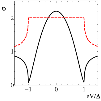
Beside the above experimental studies, a number of theories of tunneling spectroscopy in normal metal/spin-triplet chiral -wave superconductor junctions were formulated.[39, 40, 41, 44] It was shown that the line shape of a tunneling conductance in chiral -wave superconductor junctions has a broad ZBCP (see Fig. 2) due to the ABS with linear dispersion.
These theories could explain the experimental results like curve (b) in Fig. 1. However, this simple picture can not give reasonable explanation for zero bias dip like curve (a) and two-step peak like curve (c) in Fig. 1. While the origin of zero bias dip can be explained by mismatch of the Fermi surface [45] or the anisotropy of the pair potential in momentum space,[46] there are no theories which elucidate the origin of two-step peak in conductance. If the two-step peak in conductance comes from intrinsic nature of the superconducting Sr2RuO4, then one possibility for this origin is the multi-band effect. It is well known that this material has a two-dimensional electronic structure where cylindrical Fermi surfaces are formed by three bands, , , and sheets, which mainly originate from the Ru orbitals.[7] The -band is mainly composed of two-dimensional -orbital while and -bands are mainly composed of quasi-one-dimensional and -orbitals. Due to this difference of the orbital nature, it is natural to consider that the energy gap in each orbital is different. This difference of the energy scale might produce the two-step peak. Actually, several microscopic mechanisms of superconductivity in Sr2RuO4 are proposed based on multi-orbital model as well as single band model.[47, 48, 49, 50, 51, 52] Some of these theories stress the superconductivity which stems from the two-dimensional -band,[53, 54, 55, 56, 57] while there are theories where the quasi-one-dimensional and -bands were addressed.[58, 59, 60, 61] Still, a theory of conductance considering multi-orbital effect is lacking.
In taking into account the multi-orbital effect on the conductance quantitatively, one has to work with realistic band structures based on microscopic considerations.[62] A number of theoretical studies addressed superconductivity in the -wave or -wave pairing in the framework of tight binding model.[63, 64, 65, 66, 67, 68, 69] However, this approach suffers from the problem of the existence of two different energy scales: transfer integral and the pair potential. Usually, the magnitude of transfer integral is two to three orders of magnitude larger than that of the pair potential. Owing to the limitations of computational resources, one can not obtain reliable data of conductance in a finite size system if we choose the realistic values of , since, the coherence length is large and finite-size effect becomes distinct. Since many exotic properties have been predicted in spin-triplet -wave superconductor junctions,[70, 71, 72, 73, 74, 75] it is quite urgent task to calculate SDOS and in spin-triplet chiral -wave superconductors based on a microscopic model while taking into account electronic structures of Sr2RuO4 and realistic magnitude of pair potentials.
In this paper, we calculate the SDOS and of Sr2RuO4 based on the three-band model using the Green’s function method for semi-infinite system. This approach is free from the problem of finite-size effect, and therefore one can choose the realistic magnitude of superconducting pair potential. For band, we assume two-dimensional chiral -wave pair potential for all the cases we have studied. For and bands, we study two kinds of pair potentials: two-dimensional pair potentials and quasi-one-dimensional ones. In two-dimensional model, the calculated SDOS () shows a zero energy (zero bias) dip. In the presence of a spin-orbit interaction (SOI), from atomic origins, a small zero energy (zero bias) peak inside dip-like structure in SDOS () appears for the two-dimensional model. For the quasi-one-dimensional model, where the pair potential from -band is dominant, the obtained SDOS () shows a zero energy (zero bias) peak in the absence of SOI. On the other hand, this zero energy (zero bias) peak of the SDOS() is suppressed by the SOI. In the case of quasi-one-dimensional model where the pair potentials from and -bands are dominant, the resulting shows a two-step zero bias peak. The experimentally obtained two-step structure with sharp ZBCP can be explained by this quasi-one-dimensional model.
The organization of this paper is as follows. In Sec. 2 we discuss the general formulation of the recursive Green’s function. In Sec. 3, we show the calculated results of SDOS and by the recursive Green’s function. We also show Andreev bound states obtained in finite system to understand SDOS and in detail. Sec. 4 provides the summary of our paper.
2 Model and Formulations
In this section, we introduce a three-band model for Sr2RuO4 and briefly review the recursive Green’s function method combined with Mbius transformation proposed by Umerski.[76]
2.1 Three-band model for Sr2RuO4
In Sr2RuO4, three cylindrical Fermi surface called -, - and -bands are obtained by the first principle calculations or ARPES measurements. A tight-binding model considering the -, - and -orbitals can describe these band structures,
| (1) |
The first term expresses the kinetic energy,
| (2) |
where, is the annihilation operators with momentum and spin (-) for - and -orbitals (-orbital). Considering the hopping integral up to next nearest neighbor sites, the components of Eq. (2) are given by,
| (3) | ||||
| (4) | ||||
| (5) | ||||
| (6) |
The second term describes an atomic SOI which causes a mixture of spin and orbital,
| (7) |
where, () for (). The last term denotes the condensation energy due to the formation of Cooper pairs. In the superconducting state of Sr2RuO4, the most promising candidate of the pair potential belongs to the irreducible representation.[7, 16] In this irreducible representation, we consider the intraorbital pairing,
| (8) |
where, denotes the orbital index. Considering the crystal symmetry of Sr2RuO4 and the orbital nature, we study two kinds of pair potentials. The first case is the two-dimensional pair potentials,
| (11) |
Since the - and -orbitals have quasi-one-dimensional nature, hence we choose another possibility which we call the quasi-one-dimensional pair potentials,
| (15) |
2.2 Recursive Green’s function method
Starting from the Hamiltonian introduced in the previous section, we calculate local Green’s function at the surface of semi-infinite Sr2RuO4 layer. For this purpose, we use recursive Green’s function method using Mbius transformation proposed by Umerski.[76] For semi-infinite layer, we consider the clean and homogeneous system with a flat (100) surface at . Then, we can assume that the momentum parallel to the surface, , is a good quantum number and the system is one-dimensional chain for each . To calculate the surface Green’s function at and complex frequency , we first define the following matrix,
| (16) |
where, is a unit matrix. and are matrices of local term and non-local term in the Hamiltonian, respectively. The size of the Hamiltonian is including three, two and two degrees of freedom for orbital, spin and electron-hole spaces, respectively, i.e., the size of the matrix is . After diagonalization of by the eigenmatrix ,
| (17) |
with , we obtain the surface Green’s function in the following form,
| (18) |
where and are the submatrices of
| (19) |
From the poles of this surface Green’s function inside the energy gap, we can evaluate the dispersion of the ABSs. We can also evaluate the SDOS by the imaginary part of the retarded Green’s function,
| (20) |
where is an infinitesimal imaginary part. For the trace in Eq. (20), we only sum up the electronic part and drop the contribution due to the holes. Next, we calculate the conductance in normal metal/superconducting Sr2RuO4 junction. In the normal metal, we consider a two-dimensional single-band model with the energy dispersion given by , where () is the transfer integral between (next) nearest neighbor sites. To calculate the conductance, we first obtain the surface Green’s functions for normal metal at and for Sr2RuO4 at in the absence of the interface hoppings, and we obtain the local and the non-local Green’s functions in normal metal/superconducting Sr2RuO4 junction,
| (21) | |||||
| (22) | |||||
| (23) | |||||
| (24) |
where, and are the hopping matrices at the interface. From these Green’s functions, we obtain the conductance by using the Kubo formula.[77, 78] Since we start from the BdG Hamiltonian, which is not the eigenstate of the particle number, for Sr2RuO4, the electric current is not conserved inside the superconductor unless either a source term is added or self-consistency due to proximity effect is included.[79] To avoid this problem, in the actual calculation, we calculate the expectation values of the current operator inside the normal metal, where the source term is absent. Note that known single band results in the absence of SOI[46] are reproduced in the present three band model if we just introduce the interface hopping between normal metal and dxy-orbital in Sr2RuO4.
3 Results
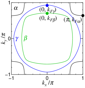
In this section, we show the calculated results of the dispersion of ABSs, SDOS and conductance. Prior to that, we explain the choice of parameters. We have set as a unit of energy, and for other hopping parameters in Sr2RuO4, we choose , , and as adopted in the previous studies.[56, 80] The obtained Fermi surfaces using these parameters are shown in Fig. 3, in which the Fermi momenta in -direction , and are defined for convenience. For the SOI , we adopt the value estimated from the quasiparticle spectra of angle resolved photoemission spectroscopy et al.[81] The obtained values of in Ref. \citenZabolotnyy is and , which correspond to and , respectively, by using the values of and in the above. Though is the plausible value by the above estimation, we also show the results of ABSs and conductance for , and to clarify the effect of the SOI. The chemical potentials are determined to set the number of electron to be per spin. For the magnitude of the pair potential we choose which is comparable to the critical temperature of Sr2RuO4. For the hopping parameters and the chemical potential in the normal metal, we choose , and , which are the same as those for -orbital without the SOI (-band).
In the later subsections, we present the results for following three cases: The first one is the two-dimensional pair potential as shown in Eq.(11) with and . This is a simple expansion of a single band model considering -band.[48, 49, 82] The second is the quasi-one-dimensional pair potential as shown in Eq.(15) with and . This pair potential includes quasi-one-dimensional nature of and -bands, while the dominant pairing is composed of -band.[53, 54, 56] Finally, the quasi-one-dimensional pair potential is same as the second one but with and . In this case, the dominant pairing comes from and -bands.[61, 68, 69]
3.1 Two-dimensional pair potential
In this subsection, we consider the case of two-dimensional pair potential, where the pair potential of each orbital is shown in Eq. (11). For the magnitude of the pair potential, we choose and in accordance with theoretical results by Nomura and Yamada.[56, 80] The interface hoppings in normal metal/Sr2RuO4 junction are chosen as () for high (low) transmissivity.
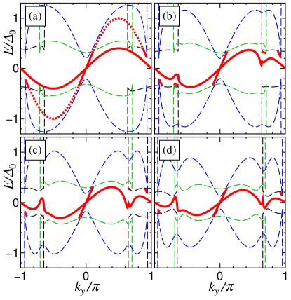
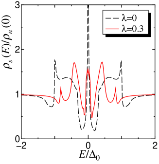
The calculated dispersion of ABSs is shown in Fig. 4. Since Sr2RuO4 has a mirror symmetry, the Hamiltonian of Sr2RuO4 is divided into two mirror sectors.[83] In Fig. 4, we show the ABSs for one of the mirror sectors. The ABSs for the other sector is obtained by the particle-hole transformation, i.e. . In the absence of SOI, there are three ABS originating from , , and -bands as shown in Fig. 4 (a). Dispersions of these three ABS is represented by () for and -bands (-band). Note that the ABSs that originate from and -bands are degenerate at ; where, and are the Fermi momenta shown in Fig. 3. This degeneracy is lifted by SOI and one of the ABS disappears at as shown in Figs. 4 (b)-(d). In these lifted ABSs, the one with the higher-energy disappears as increasing the magnitude of SOI. The lower-energy one is strongly suppressed and it crosses the Fermi level for . Next, we show calculated results for the SDOS and conductance in Figs. 5 and 6, respectively. Without the SOI, SDOS shows a zero energy dip surrounded by four peaks at around and . The position of the peaks corresponds to the energy levels of the ABSs at around where their slope become to be zero. These features are essentially the same as the single band results considering the pair potential .[46] Further, in low transmissivity has a zero bias dip and four peaks at , similar to the SDOS as seen from solid line in Fig. 6(a). Though these four peaks are smeared in high transmissivity, still has a dip-like structure at . On the other hand, SDOS in the presence of SOI has zero bias peak since the diepersion of ABS at is close to the Fermi levels. It also have many small spikes reflecting the complex structure of the energy dispersion of the ABS. in the presence of SOI has a zero bias peak for both high and low transmissivity as seen from Fig. 6(b)-(d). In the case of low transmissivity, as compared to without SOI, the positions of peaks in with SOI other than zero bias peak shift to lower energy and the height of the peaks becomes lower due to the suppression of the bulk energy gap. In the case of high transmissivity, three peaks merge and shows a single ZBCP.
3.2 Quasi-one-dimensional pair potential
Here, we consider the case of quasi-one-dimensional pair potential where the pair potential of each orbital is given by Eq. (15). We consider two choices for the magnitude of the pair potentials. One is the case with , . This pair potential well reproduces Nomura and Yamada’s results[56, 80] not only for the magnitude of pair potential but for the momentum dependence of the pair potential on the Fermi surface. The other case is , to emphasize the importance of the quasi-one-dimensional band as suggested by some microscopic models.[61, 68, 69]
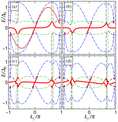
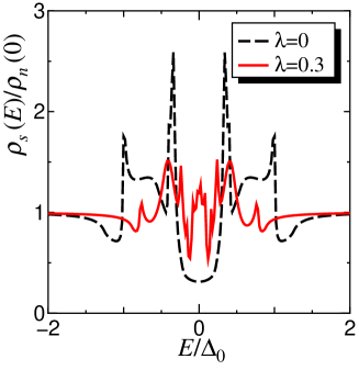
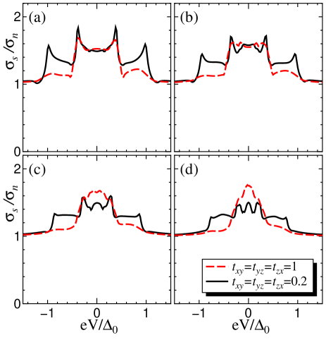
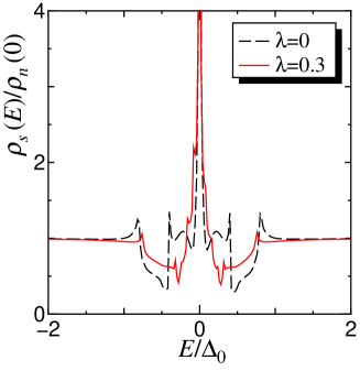
First, we consider the case for and without the SOI. Without SOI, bulk energy gap and dispersion of ABS (7(a)) originating from -band are the same as in the case of two-dimensional pair potential (Fig. 4(a)) because the pair potential for -orbital are the same. On the other hand, the dispersion of chiral edge modes originating from and -bands are almost flat at around and . This can be understood as follows: On the Fermi surface of - and -bands, where azimuthal angles measured from the center of the Fermi surfaces are from to , i.e. at around (-band) and (-band), their dominant components of orbitals are -orbital, whose pair potential is proportional to like -wave. It is known that the system has zero energy ABS on (100) surface for -wave pair potential due to the -phase shift of the pair potential between incident and reflected quasi-particles.[64, 84, 85, 86] This one-dimensional nature remains even in the presence of the mixture of and -orbitals. For this reason, the energy levels of the ABS near and is nearly zero. With increasing the magnitude of the SOI, quasi-one-dimensional nature of the ABS disappears due to the coupling with -orbital as seen from Figs. 7(b)-(d). Due to the level repulsion between the ABSs originating from -band and -bands, the group velocity of the ABS of -bands at becomes negative. The resulting SDOS and conductance are shown in Fig. 8 and Fig. 9, respectively. SDOS at low energy and in low bias voltage (e.g. and , respectively) drastically change as compared to those with two-dimensional pair potential. SDOS in the absence of the SOI shows a sharp zero energy peak due to the quasi-one-dimensional nature of the ABS as seen from dashed line in Fig. 8. A similar line shape is also found in in the low transmissivity for up to 0.2(Fig. 9(a)-(c)). In contrast, this sharp zero energy (bias) peak in SDOS ( in low transmissivity) suppressed for , and it shows a small zero bias dip as shown in Fig. 8 (Fig. 9(d)). In high transmissivity, shows a single zero bias peak regardless of the magnitude of the SOI.
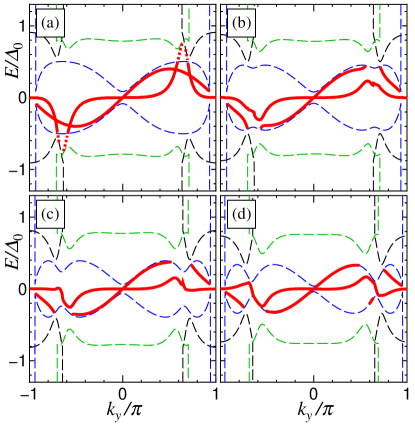

Next, we consider another choice of the magnitude of the pair potential; and . The dispersions of the ABSs without the SOI shown in Fig. 10(a) are identical with those for the previous case (Fig. 7(a)) except for the energy scales of and . Thus, the SDOS and show a sharp zero energy peak and a ZBCP similar to the case with as shown in Fig. 11 and Fig. 12(a), respectively. The dispersions of the ABSs in the presence of the SOI are shown in Figs. 10(b)-(d). In comparison with the case of in Fig. 11, the effect of the SOI on the group velocity of the ABSs at around and is small. This is because the induced two-dimensionality for the ABS originating from - -bands is small since the magnitude of the two-dimensional pair potential in -orbital is small. As a result, the SDOS and still have zero energy peak and ZBCP up to as shown in Fig. 11 and Fig. 12(b)-(d), respectively. Note that, we can not see clear dip-like structure in originating from -band under cover of strong ZBCP due to - -bands. Thus, shows the two-step peaks regardless of the magnitude of the SOI as shown in solid lines in Fig. 12.
4 Discussion and Summary
| pair potential | dominant pair | line shape of conductance |
|---|---|---|
| 2D() | Three peaks | |
| Q1D()+2D() | Tiny zero bias dip | |
| Q1D()+2D() | Two-step peak | |
| - | single ZBCP | |
| - | Zero bias dip |
In table 1, we show our results of the line shapes of conductance for in the three-band model as well as those in a single-band model in the previous studies[39, 40, 46]. Here, we compare the calculated results with experimental data shown in Fig. 1. Two-step ZBCP structure like curve (c) in Fig. 1 only appears for quasi-one-dimensional pair potential with (see Fig. 12). We shall discuss the strength of the SOI here. In Ref. \citenHaverkort, the band dispersion of Sr2RuO4 has been studied by the first principle calculation including the SOI. The obtained value of the energy-level splitting at -point between and -bands is about 90meV. In the present model, by choosing the unit of the energy to be 230meV, we can reproduce the energy level of the and -bands at -point. The obtained values of the energy-level splitting are , and meV for , 0.2 and 0.3, respectively. If we simply see this result, is the appropriate choice of the SOI. In this case, two-step ZBCP also appears for the quasi-one-dimensional pair potential with as shown in Fig. 9(c). However, the electron correlation which is not fully taken into account in the local density approximation might induce the renormalization of the quasiparticle energy bands and the effective values of becomes about as mentioned in Sec. 3. In either case of or , two-step ZBCP never appears for the two-dimensional pair potential but for the quasi-one-dimensional pair potential.
As for a broad ZBCP like curve (b) in Fig. 1, a junction with high transmissivity shows this for all pairings considered in the present paper since the Andreev reflection process governs the conductance in the energy gap. A single ZBCP also appears when the size of the Fermi surface is small and/or the insulating barrier potential is high. In these cases, the contribution of the perpendicular injection () is enhanced, where the energy levels of the ABSs are close to zero for all the pairing considered in the present study. However, the former is not likely in the present case since it is known that the size of the Fermi surface of Gold is large.
Besides, we have also confirmed that dip-like structure as shown in curve (a) in Fig. 1 is reproduced if we ignore the interface hoppings to - and -orbitals, though the mechanism to realize this situation is unclear. Nevertheless, if only the -band contributes to the conductance, dip-like structure appears as explained in Ref. \citenSengupta. Another possibility of the emergence of a zero bias dip is the -axis tunneling, where there is no ABS and a conventional gap structure appears. However, the junctions which are used in the measurements of the conductance, have been made at the position without the -axis tunneling by measuring the interface by the scanning ion microscopy. Therefore, the contribution of the -axis tunneling is excluded below the resolution.
In this paper, we have studied ABSs, SDOS and of Sr2RuO4 based on the three band model using recursive Green’s function. For -orbital, we assume two-dimensional chiral -wave pair potential for all cases we have studied. For and -orbital we have studied two kinds of pair potentials: two-dimensional pair potentials and quasi-one-dimensional ones. In the former case, we have chosen , and for the latter, and . For a two-dimensional model, the calculated SDOS () shows a zero energy (bias) dip without the SOI. In the presence of the SOI, small zero energy (bias) peak inside dip-like structure in SDOS() appears. While, in the quasi-one-dimensional model with , the obtained SDOS () shows a zero energy (bias) peak. This zero energy (bias) peak in SDOS () is suppressed by the SOI. In the case of , the resulting shows a two-step zero bias peak with sharp ZBCP and broad one. The last one can reasonably explain the experimental data. We do not consider the roughness of the surface and disorder. Since the pairing symmetry is influenced by these effects, it is necessary to construct more realistic theory taking account of these effects in the future.
We gratefully acknowledge M. Sato, A. Yamakage, I. A. Devyatov, A. V. Burmistrova and S. Onari for valuable discussions, and we thank A. Dutt for critical reading of the manuscript. This work was supported in part by a Grant-in Aid for Scientific Research from MEXT of Japan, ”Topological Quantum Phenomena” Grants No. 22103005 and No. 20654030 (Y.T.), Dutch Foundation for Fundamental Research on Matter (FOM) and by EU-Japan program ”IRON SEA”, and Russian Ministry of Education and Science.
References
- [1] Y. Maeno, H. Hashimoto, K. Yoshida, S. Nishizaki, T. Fujita, J. G. Bednorz, and F. Lichtenberg: Nature 372 (1994) 532.
- [2] K. Ishida, H. Mukuda, Y. Kitaoka, K. Asayama, Z. Q. Mao, Y. Mori, and Y. Maeno: Nature 396 (1998) 658.
- [3] H. Mukuda, K. Ishida, Y. Kitaoka, Z. Mao, Y. Mori, and Y. Maeno: J. Low Temp. Phys. 117 (1999) 1587.
- [4] K. Ishida, H. Mukuda, Y. Kitaoka, Z. Q. Mao, H. Fukazawa, and Y. Maeno: Phys. Rev. B 63 (2001) 060507.
- [5] H. Murakawa, K. Ishida, K. Kitagawa, Z. Q. Mao, and Y. Maeno: Phys. Rev. Lett. 93 (2004) 167004.
- [6] G. M. Luke, Y. Fudamoto, K. M. Kojima, M. I. Larkin, J. Merrin, B. Nachumi, Y. J. Uemura, Y. Maeno, Z. Q. Mao, Y. Mori, H. Nakamura, and M. Sigrist: Nature 394 558.
- [7] A. P. Mackenzie and Y. Maeno: Rev. Mod. Phys. 75 (2003) 657.
- [8] G. E. Volovik: JETP Lett. 66 (1997) 522.
- [9] A. Furusaki, M. Matsumoto, and M. Sigrist: Phys. Rev. B 64 (2001) 054514.
- [10] X.-L. Qi and S.-C. Zhang: Rev. Mod. Phys. 83 (2011) 1057.
- [11] Y. Tanaka, M. Sato, and N. Nagaosa: J. Phys. Soc. Jpn. 81 (2012) 011013.
- [12] J. Alicea: Rep. Prog. Phys. 75 (2012).
- [13] M. Sato: Phys. Rev. B 79 (2009) 214526.
- [14] M. Sato: Phys. Rev. B 81 (2010) 220504(R).
- [15] M. Matsumoto and M. Sigrist: J. Phys. Soc. Jpn. 68 (1999) 3120.
- [16] Y. Maeno, S. Kittaka, T. Nomura, S. Yonezawa, and K. Ishida: J. Phys. Soc. Jpn. 81 (2012) 011009.
- [17] C. Kallin: Reports on Progress in Physics 75 (2012) 042501.
- [18] Y. Tanaka and S. Kashiwaya: Phys. Rev. Lett. 74 (1995) 3451.
- [19] S. Kashiwaya and Y. Tanaka: Rep. Prog. Phys. 63 (2000) 1641.
- [20] C. R. Hu: Phys. Rev. Lett. 72 (1994) 1526.
- [21] S. Kashiwaya, Y. Tanaka, M. Koyanagi, H. Takashima, and K. Kajimura: Phys. Rev. B 51 (1995) 1350.
- [22] S. Kashiwaya, Y. Tanaka, N. Terada, M. Koyanagi, S. Ueno, L. Alff, H. Takashima, Y. Tanuma, and K. Kajimura: J. Phys. Chem. Solid 59 (1998) 2034.
- [23] M. Covington, M. Aprili, E. Paraoanu, L. H. Greene, F. Xu, J. Zhu, and C. A. Mirkin: Phys. Rev. Lett. 79 (1997) 277.
- [24] L. Alff, H. Takashima, S. Kashiwaya, N. Terada, H. Ihara, Y. Tanaka, M. Koyanagi, and K. Kajimura: Phys. Rev. B 55 (1997) R14757.
- [25] J. Y. T. Wei, N.-C. Yeh, D. F. Garrigus, and M. Strasik: Phys. Rev. Lett. 81 (1998) 2542.
- [26] I. Iguchi, W. Wang, M. Yamazaki, Y. Tanaka, and S. Kashiwaya: Phys. Rev. B 62 (2000) R6131.
- [27] A. Biswas, P. Fournier, M. M. Qazilbash, V. N. Smolyaninova, H. Balci, and R. L. Greene: Phys. Rev. Lett. 88 (2002) 207004.
- [28] B. Chesca, H. J. H. Smilde, and H. Hilgenkamp: Phys. Rev. B 77 (2008) 184510.
- [29] M. D. Upward, L. P. Kouwenhoven, A. F. Morpurgo, N. Kikugawa, Z. Q. Mao, and Y. Maeno: Phys. Rev. B 65 (2002) 220512.
- [30] C. Lupien, S. K. Dutta, B. I. Barker, Y. Maeno, and J. C. Davis: arXiv:cond-mat/0503317 .
- [31] Y. Pennec, N. J. C. Ingle, I. S. Elfimov, E. Varene, Y. Maeno, A. Damascelli, and J. V. Barth: Phys. Rev. Lett. 101 (2008) 216103.
- [32] H. Suderow, V. Crespo, I. Guillamon, S. Vieira, F. Servant, P. Lejay, J. Brison, and J. Flouquet: New J. Phys. 11 (2009) 093004.
- [33] I. A. Firmo, S. Lederer, C. Lupien, A. P. Mackenzie, J. C. Davis, and S. A. Kivelson: Phys. Rev. B 88 (2013) 134521.
- [34] F. Laube, G. Goll, H. v. Löhneysen, M. Fogelström, and F. Lichtenberg: Phys. Rev. Lett. 84 (2000) 1595.
- [35] S. Kashiwaya, H. Kashiwaya, H. Kambara, T. Furuta, H. Yaguchi, Y. Tanaka, and Y. Maeno: Phys. Rev. Lett. 107 (2011) 077003.
- [36] Z. Q. Mao, K. D. Nelson, R. Jin, Y. Liu, and Y. Maeno: Phys. Rev. Lett. 87 (2001) 037003.
- [37] M. Kawamura, H. Yaguchi, N. Kikugawa, Y. Maeno, and H. Takayanagi: J. Phys. Soc. Jpn. 74 (2005) 531.
- [38] K. Deguchi, Z. Q. Mao, and Y. Maeno: J. Phys. Soc. Jpn. 73 (2004) 1313.
- [39] M. Yamashiro, Y. Tanaka, and S. Kashiwaya: Phys. Rev. B 56 (1997) 7847.
- [40] M. Yamashiro, Y. Tanaka, Y. Tanuma, and S. Kashiwaya: J. Phys. Soc. Jpn. 67 (1998) 3224.
- [41] C. Honerkamp and M. Sigrist: J. Low Temp. Phys. 111 (1998) 895.
- [42] M. Sigrist and H. Monien: Journal of the Physical Society of Japan 70 (2001) 2409.
- [43] S. Kashiwaya: Unpublished .
- [44] A. Akbari and P. Thalmeier: Phys. Rev. B 88 (2013) 134519.
- [45] S. Wu and K. V. Samokhin: Phys. Rev. B 81 (2010) 214506.
- [46] K. Sengupta, H.-J. Kwon, and V. M. Yakovenko: Phys. Rev. B 65 (2002) 104504.
- [47] T. M. Rice and M. Sigrist: Journal of Physics: Condensed Matter 7 (1995) L643.
- [48] K. Miyake and O. Narikiyo: Phys. Rev. Lett. 83 (1999) 1423.
- [49] T. Nomura and K. Yamada: J. Phys. Soc. Jpn. 69 (2000) 3678.
- [50] T. Kuwabara and M. Ogata: Phys. Rev. Lett. 85 (2000) 4586.
- [51] R. Arita, S. Onari, K. Kuroki, and H. Aoki: Phys. Rev. Lett. 92 (2004) 247006.
- [52] S. Onari, R. Arita, K. Kuroki, and H. Aoki: J. Phys. Soc. Jpn. 74 (2005) 2579.
- [53] T. Nomura and K. Yamada: J. Phys. Soc. Jpn. 71 (2002) 404.
- [54] T. Nomura and K. Yamada: J. Phys. Soc. Jpn. 71 (2002) 1993.
- [55] Y. Yanase and M. Ogata: J. Phys. Soc. Jpn. 72 (2003) 673.
- [56] T. Nomura: J. Phys. Soc. Jpn. 74 (2005) 1818.
- [57] Q. H. Wang, C. Platt, Y. Yang, C. Honerkamp, F. C. Zhang, W. Hanke, T. M. Rice, and R. Thomale: EPL (Europhysics Letters) 104 (2013) 17013.
- [58] M. Sato and M. Kohmoto: J. Phys. Soc. Jpn. 69 3505.
- [59] K. Kuroki, M. Ogata, R. Arita, and H. Aoki: Phys. Rev. B 63 (2001) 060506.
- [60] T. Takimoto: Phys. Rev. B 62 (2000) R14641.
- [61] S. Raghu, A. Kapitulnik, and S. A. Kivelson: Phys. Rev. Lett. 105 (2010) 136401.
- [62] A. V. Burmistrova, I. A. Devyatov, A. A. Golubov, K. Yada, and Y. Tanaka: J. Phys. Soc. Jpn. 82 (2013) 034716.
- [63] Y. Tanuma, K. Kuroki, Y. Tanaka, R. Arita, S. Kashiwaya, and H. Aoki: Phys. Rev. B 66 (2002) 094507.
- [64] Y. Tanuma, K. Kuroki, Y. Tanaka, and S. Kashiwaya: Phys. Rev. B 64 (2001) 214510.
- [65] Y. Tanuma, Y. Tanaka, M. Ogata, and S. Kashiwaya: Phys. Rev. B 60 (1999) 9817.
- [66] J.-X. Zhu and C. S. Ting: Phys. Rev. B 61 (2000) 1456.
- [67] Y. Asano: Phys. Rev. B 63 (2001) 052512.
- [68] Y. Imai, K. Wakabayashi, and M. Sigrist: Phys. Rev. B 85 (2012) 174532.
- [69] Y. Imai, K. Wakabayashi, and M. Sigrist: Phys. Rev. B 88 (2013) 144503.
- [70] Y. Tanaka and S. Kashiwaya: Phys. Rev. B 70 (2004) 012507.
- [71] Y. Tanaka, S. Kashiwaya, and T. Yokoyama: Phys. Rev. B 71 (2005) 094513.
- [72] Y. Asano, Y. Tanaka, and S. Kashiwaya: Phys. Rev. Lett. 96 (2006) 097007.
- [73] Y. Tanaka, Y. V. Nazarov, and S. Kashiwaya: Phys. Rev. Lett. 90 (2003) 167003.
- [74] Y. Tanaka, Y. Asano, A. A. Golubov, and S. Kashiwaya: Phys. Rev. B 72 (2005) 140503.
- [75] Y. Tanaka and A. A. Golubov: Phys. Rev. Lett. 98 (2007) 037003.
- [76] A. Umerski: Phys. Rev. B 55 (1997) 5266.
- [77] Y. Takane and H. Ebisawa: J. Phys. Soc. Jpn. 61 (1992) 1685.
- [78] P. A. Lee and D. S. Fisher: Phys. Rev. Lett. 47 (1981) 882.
- [79] H. Ohta and C. Ishii: Mesoscopic Josephson Junctions (The Physical Society of Japan, 1999).
- [80] T. Nomura, D. S. Hirashima, and K. Yamada: J. Phys. Soc. Jpn. 77 (2008) 024701.
- [81] V. Zabolotnyy, D. Evtushinsky, A. Kordyuk, T. Kim, E. Carleschi, B. Doyle, R. Fittipaldi, M. Cuoco, A. Vecchione, and S. Borisenko: Journal of Electron Spectroscopy and Related Phenomena 191 (2013) 48 .
- [82] T. Kuwabara and M. Ogata: Phys. Rev. Lett. 85 (2000) 4586.
- [83] Y. Ueno, A. Yamakage, Y. Tanaka, and M. Sato: Phys. Rev. Lett. 111 (2013) 087002.
- [84] J. Hara and K. Nagai: Prog. Theor. Phys. 76 (1986) 1237.
- [85] K. Sengupta, I. Žutić, H.-J. Kwon, V. M. Yakovenko, and S. Das Sarma: Phys. Rev. B 63 (2001) 144531.
- [86] L. J. Buchholtz and G. Zwicknagl: Phys. Rev. B 23 (1981) 5788.
- [87] M. W. Haverkort, I. S. Elfimov, L. H. Tjeng, G. A. Sawatzky, and A. Damascelli: Phys. Rev. Lett. 101 (2008) 026406.