Hysteretic electrical transport in BaTiO3/Ba1-xSrxTiO3/Ge heterostructures
Abstract
We present electrical transport measurements of heterostructures comprised of BaTiO3 and Ba1-xSrxTiO3 epitaxially grown on Ge. The Sr-alloying imparts compressive strain to the BaTiO3, which enables the thermal expansion mismatch between BaTiO3 and Ge to be overcome to achieve -axis oriented growth. The conduction bands of BaTiO3 and Ba1-xSrxTiO3 are nearly aligned with the conduction band of Ge, which facilitates electron transport. Electrical transport measurements through the dielectric stack exhibit rectifying behavior and hysteresis, where the latter is consistent with ferroelectric switching.
pacs:
74.50.+r, 74.72.Bk, 74.20.Rp, 74.25.NfRecent advancements in epitaxial growth have enabled single crystalline ferroelectrics to be integrated with conventional semiconductors, opening a pathway to exploit the polarization of the former in semiconducting based devices. Electrically coupling the re-orientable polarization of a ferroelectric to a semiconducting channel remains a long standing challenge in materials research. Single crystalline ferroelectrics on semiconductors are ideal for such applications, since they offer superior material characteristics in comparison to polycrystalline materials Lin ; Demkov . Ferroelectric - semiconductor heterojunctions were originally conceived to operate as capacitors, where the polarization could be utilized to maintain accumulation or depletion in the semiconducting electrodeDawber . In such an application, DC charge transport through the ferroelectric gate stack is inhibited. However, ferroelectric thin films also exhibit semiconducting properties, which could provide additional functionality in ferroelectric - semiconductor heterostructures Zubko ; Bratkovsky ; Morozovska ; Alpay . In conjunction with the re-orientable polarization, the semiconducting properties of thin film ferroelectrics could potentially be utilized to control charge transport through ferroelectric-semiconductor heterojunctions.
In this letter, we introduce mobile carriers into a ferroelectric-semiconductor heterostructure and exploit the re-orientable polarization to modulate the Schottky barrier to a semiconductor. Our heterostructures are comprised of BaTiO3 (BTO) and Ba1-xSrxTiO3 (BST) grown epitaxially on a Ge wafer, with Pt serving as the counter electrode. X-ray photoemission spectroscopy measurements indicate that the conduction bands of Ge and BTO are nearly aligned, thus enabling charge transport through the heterojunction interface. Transport measurements of the current through the asymmetric capacitors reveals rectifying behavior and hysteresis. The former arises from the presence (absence) of a barrier at the metal-ferroelectric (ferroelectric-semiconductor) interface for charge transport, whereas the latter can be attributed to switching of the ferroelectric polarization.
The BTO/BST heterostructures were grown using reactive molecular beam epitaxy (MBE)McKee_Science ; JWReinerAdvMat . The (100)-oriented p-type (0.018 cm) Ge wafers were cleaned by dipping in a 30:1 solution of H2O:HF for 60 s, followed by exposure to UV light for 30 s. The wafers were then introduced into the ultra-high vacuum MBE chamber and heated to 500 to remove the native GeO2 layer. A clean, dimerized Ge surface was confirmed by the appearance of a 2 1 reconstruction along the [11] direction of the Ge surface in the RHEED pattern. A half monolayer mix of 60:40 Ba:Sr was initially deposited on the clean Ge surface at 4500C McKee . The wafer was then cooled to room temperature where an additional half monolayer of 60:40 Ba:Sr was deposited, followed by co-deposition of 2 monolayers each of 60:40 BaO:SrO and TiO2. The wafer was then heated to 5000C in high-vacuum where the amorphous BaO/SrO and TiO2 layers reacted to form 2 unit cells of crystalline Ba0.6Sr0.4TiO3. Additional BST layers, described below, were subsequently grown on top of the crystallized 2 unit cells at a substrate temperature of 5700C and in a background O2 pressure of 3 10-7 Torr. Following growth, the heterostructures were annealed in oxygen plasma at 3900C for 30 minutes to minimize the presence of residual oxygen vacancies.
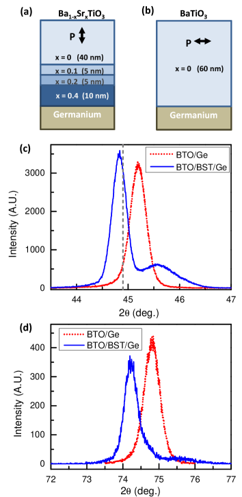
Our epitaxial BTO/BST/Ge heterostructures were designed to exhibit -axis orientation and be sufficiently thick to offset the effects of depolarization fields LinesGlass ; Tilley ; Littlewood . Depolarization fields are strong in ferroelectric/semiconductor heterojunctions due to the large screening length associated with semiconducting materials. For BTO grown on Ge, film thicknesses exceeding 40 nm are required to offset depolarization fields and maintain ferroelectric behavior JWReiner . However, maintaining -axis oriented growth for thicknesses exceeding 40 nm is challenging due to the thermal expansion mismatch between BTO and Ge. Epitaxial BTO films grown on Ge relax for thicknesses exceeding 10 nm due to the difference in lattice constants at typical growth temperatures. As relaxed films are cooled through the Curie temperature, tensile strain is imparted to the BTO from the Ge substrate, since the former has a much larger coefficient of thermal expansion than the latter. Consequently, BTO grown on Ge has -axis orientation, associated with a ferroelectric polarization that lies predominantly in the plane of the film. To achieve thick -axis oriented films with an out-of-plane polarization, we utilize Sr alloying to impart compressive strain to BTO, as shown in Fig.1(a)Schlom . Our heterostructures are comprised of 4 layers, with increasing Sr content for the layers approaching the Ge substrate. The in-plane lattice constants of the BST layers near the interface are reduced with increased Sr alloying, thus compressive strain is imparted to the BTO grown on top, resulting in -axis oriented films.
X-ray diffraction measurements taken on our heterostructures confirm -axis oriented growth. Figure 1(c) shows x-ray intensity versus 2 for a typcial BTO/BST/Ge heterostructure (blue curve). The smaller (002) peak at 2 = 45.60 arises from the 20 nm thick Sr alloyed layers near the interface, while the larger (002) peak located at 2 = 44.750 is associated with the 40 nm thick BTO top layer. For comparison, the (002) associated with bulk BTO is indicated by the dashed grey line. We note that the compressive strain induced by the Sr alloying has enhanced the out-of-plane lattice constant of our BTO films to exceed the bulk value. Figure 1(c) also shows x-ray intensity data for a 60 nm thick BTO/Ge film without the Sr alloyed layers (red dotted), schematically illustrated in Fig.1(b). The absence of Sr-alloying results in -axis oriented films with predominantly in-plane polarization. Finally, Fig.1(d) shows the (103) (blue solid) and (301) (red dotted) peaks for the BTO/BST/Ge and BTO/Ge heterostructures, respectively. Analysis of the x-ray data for the BTO/BST/Ge heterostructure indicates the out-of-plane (in-plane) lattice constant is 4.040 Å(3.987 Å).
Previous studies have shown that the band gaps of BTO and SrTiO3 are virtually identical, and that their conduction bands are nearly aligned with the conduction bands of Si and Ge Cardona ; FAmy ; Robertson . The near alignment of conduction bands at interfaces between BTO/BST and Ge facilitates charge transport and suggests that rectifying behavior should be exhibited by such heterojunctions, provided a counter electrode forming an interface with finite barrier for charge transport can be created on the BTO surface.
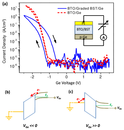
To explore the possibility of diode-like transport, Pt electrodes 28 m in diameter were deposited by electron beam evaporation through a shadow mask on the BTO surface, and 2-point electrical transport measurements were performed in the geometry illustrated in the inset of Fig.2(a). Representative current-voltage characteristics of a Pt/BTO/BST/Ge heterostructure are shown in Fig.2(a). For -axis oriented heterostructures, rectifying behavior and hysteresis is observed (blue solid). Transport characteristics of an -axis oriented Pt/BTO/Ge heterostructure are shown for comparison (red dashed), which also exhibits rectifying behavior but negligible hysteresis. The rectifying behavior arises from the asymmetry of the metal/ferroelectric/semiconductor heterojunction, namely the presence (absence) of a potential barrier at the Pt/BTO (BST/Ge) interface. For voltages applied to the Ge wafer that are -1 V, electrons flow from Ge to Pt electrodes via the BST conduction bandMinority_Generation , as illustrated in Fig.2(b). In contrast, for -1 V, a barrier arising from the workfunction of Pt inhibits holes from entering the BTO valence band, as illustrated in Fig.2(c).
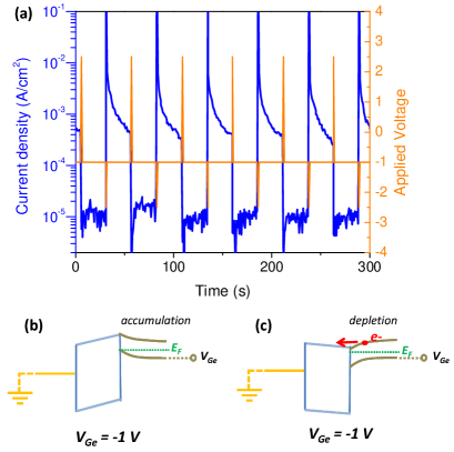
The hysteresis in the transport current for -axis oriented heterostructures exhibits characteristics that are consistent with ferroelectric switching. First, the hysteresis is present (absent) for -axis (-axis) oriented heterostructures, consistent with switching (non-switching) under electric fields that are applied co-linear with (perpendicular to) the direction of polarization. Second, the magnitude of the transport current can be switched between high and low regimes with ms duration voltage pulses centered about = -1 V, as shown in Fig.3(a). Thus the hysteresis cannot be explained by effects associated with the drift of mobile ions, since ions within dielectric stacks typically do not respond to voltage sweeps that are 5 V/s. TPMa Third, the “clockwise” direction of the hysteresis shown in Fig.2(a) is consistent with switching of the polarization, as illustrated schematically in Fig.3(b) and (c). As is swept from -2.5 V to -1 V, the polarization of the BTO causes the Ge to be near inversion, as shown in Fig.3(c). The state of near inversion, implies the absence of a Schottky barrier for minority carriers to transfer from the Ge to the BTO/BST heterostructure. In contrast, as is swept from +2.5 V to -1 V, the direction of the polarization is reversed, thus the Ge is in accumulation. In this scenario, a Schottky barrier prevents minority carriers from transferring from the Ge to the BTO/BST.
Carriers injected into the Ge through the BTO/BST barrier enables the interplay between ferroelectric and semiconducting properties to be explored. It is interesting to note that the change in transport current in response to pulsed voltages initially spans over 3 orders of magnitude but decays with time, as shown in Fig.3(a). The decay of the transport current with time could be associated with weakening of the polarization due to the presence of space chargeZubko . Alternatively, the decay could arise from depolarization fields weakening the ferroelectricityJWReiner . It should be noted that a constant field within the BTO/BST dielectric stack is shown in Fig.3(b) and (c). A more rigorous description should consider gradients in polarization and fields due to the Sr alloyingBratkovsky ; Morozovska ; Alpay . Finally, we note that the transport current effect observed in our heterostructures could potentially form the basis for a type of memory.
In summary, we have grown and performed structural and transport characterization of epitaxial, -axis oriented BTO/BST/Ge heterostructures. The thermal expansion mismatch that prevents -axis oriented growth is overcome through Sr-alloying, which imparts compressive strain to the BTO. The conduction bands of Ge and BaTiO3 are closely aligned. Transport measurements through the -axis oriented heterostructures exhibits rectifying behavior and hysteresis in the transport current. The rectifying behavior of the Pt/BTO/BST/Ge heterostructures arises from the asymmetry in band alignments at the Pt/BTO and BST/Ge interfaces, while the hysteresis exhibits characteristics that can be attributed to switching of the ferroelectric polarization.
Acknowledgements.
This work was supported by the NSF under contracts DMR-1119826 and MRSEC DMR-1309868 (CRISP).References
- (1) A. Lin, X. Hong, V. Wood, A. A. Verevkin, C. H. Ahn, R. A. McKee, F. J. Walker, E. D. Specht, Appl. Phys. Lett. 78, 2034 (2001).
- (2) C. Dubourdieu, J. Bruley, T. M. Arruda, A. Posadas, J. Jordan-Sweet, M. M. Frank, E. Cartier, D. J. Frank, S. V. Kalinin, A. A. Demkov, and V. Narayanan, Nat. Nanotech. 8, 748 (2013).
- (3) M. Dawber, K. M. Rabe, and J. F. Scott, Rev. Mod. Phys. 77, 1083 (2005).
- (4) P. Zubko, D. J. Jung, and J. F. Scott, J. Appl. Phys. 100, 114112 (2006).
- (5) A. M. Bratkovsky and A. P. Levanyuk, Phys. Rev. B 61, 15042 (2000).
- (6) A. N. Morozovska and E. A. Eliseev, Phys. Stat. Sol. B 242, 947 (2005).
- (7) M. B. Okatan, J. V. Mantese, and S. P. Alpay, Acta Mat. 58, 39 (2010).
- (8) J. W. Reiner, A. M. Kolpak, Y. Segal, K. F. Garrity, S. Ismail-Beigi, C. H. Ahn, and F.J. Walker, Adv. Mat. 22, 2919 (2010).
- (9) R. A. McKee, F.J. Walker, and M.F. Chisholm, Science 293, 468 (2001).
- (10) R. A. McKee, F. J. Walker, and M. F. Chisholm, Phys. Rev. Lett. 81, 3014 (1998).
- (11) M. E. Lines and A. M. Glass, Principles and Applications of Ferroelectrics and Related Materials, Oxford University Press Inc., New York (2001).
- (12) D. L. Tilley: Phase transitions in thin films, in Ferroelectric Ceramics, N. Setter, E. L. Colla (Eds.), Birkhauser Verlag, Basel (1993).
- (13) P. Chandra and P. B. Littlewood, Physics of Ferroelectrics: A Modern Perspective, K. M. Rabe, C. H. Ahn, J.-M. Triscone (Eds.), Springer-Verlag, Berlin (2007).
- (14) J. W. Reiner, F. J. Walker, R. A. McKee, C. A. Billman, J. Junquera, K. M. Rabe, and C. H. Ahn, Phys. Stat. Sol. B 241, 2287 (2004).
- (15) V. Vaithyanathan, J. Lettieri, W. Tian, A. Sharan, A. Vasudevarao, Y. L. Li, A. Kochhar, H. Ma, J. Levy, P. Zschack, J. C. Woicik, L. Q. Chen, V. Gopalan, D. G. Schlom, J. Appl. Phys. 100, 024108 (2006).
- (16) M. Cardona, Phys. Rev. 140, 651 (1965).
- (17) F. Amy, A. S. Wan, A. Kahn, F. J. Walker, and R. A. McKee, J. Appl. Phys. 96, 1635 (2004).
- (18) J. Robertson, J. Vac. Sci. Technol. B 18, 1785 (2000).
- (19) Minority carriers are assumed to be generated through the usual mechanisms involving bulk defects. See Metal Oxide Semiconductor Physics and Technology, E. H. Nicollian J. R. Brews, pg. 107.
- (20) J. -P. Han and T. P. Ma, Appl. Phys. Lett. 72, 1185 (1998).