Influence of an electron-beam exposure on the surface plasmon resonance of gold nanoparticles
Abstract
Electron beam imaging is a common technique used for characterizing the morphology of plasmonic nanostructures. During the imaging process, the electron beam interacts with traces of organic material in the chamber and produces a well-know layer of amorphous carbon over the specimen under investigation. In this paper, we investigate the effect of this carbon adsorbate on the spectral position of the surface plasmon in individual gold nanoparticles as a function of electron exposure dose. We find an optimum dose for which the plasmonic response of the nanoparticle is not affected by the imaging process. The final publication is available at link.springer.com
I Introduction
Sensing based upon the spectral wandering of localized surface plasmon resonances supported by metal nanoparticles is a major field of research and development Stewart08 ; Hafnerreview ; HalasReview . By a synthetic engineering of the plasmon field, the sensitivity has now reached the detection level of a single molecule and a unique binding event quidantACS09 ; Hafner10 ; Zijlstra12 ; Sonnichsen12 . The development of sensitive plasmonic assays and the understanding of their optical responses was largely fostered by a precise knowledge of the morphology of the sensor. In this respect, electron microscopy is a routine technique for measuring interacting distances, determining shape anisotropy or simply observing the results of a synthesis Hartland08 ; Liu2011 ; Margueritat ; Halas12 ; Rogach . However, when the accelerated electrons hit the specimen under observation, they not only produce secondary electrons pertaining information about the sample, but also interacts with carbon-containing residues inevitably present on the sample surface and in the vacuum chamber Isabell99 . Depending on the imaging condition, this interaction produces an hydrocarbon buildup covering the surface of the sample being imaged. Although this carbon uptake can be carefully controlled to fabricate plamonic structures quidant10 , nanotips for field emission Schiffmann93 ; Antognozzi97 ; Johnson02 or to serve as a mask for negative resist processes Djenizian03 , it gradually reduces the imaging contrast and causes spectroscopic artefacts Griffiths10 . The deposition of such carbonaceous film during imaging process is evidently of great concern for plasmonic sensors because of their extreme sensitivity to surface adsorbate quidantACS09 ; Hafner10 ; Zijlstra12 ; Sonnichsen12 . Strategies to alleviate film growth requires carbon volatilization in environmental SEMs toth09 or usage of oxygen plasma etching device Isabell99 ; Ebisawa ; Vane12 . Their efficiency however depend on operating conditions and may not always mitigate the effect of an electron-beam induced carbon deposition.
In this paper, we evaluate the effect of a carbon contamination consequent of an electron-beam exposure on the surface plasmon resonance of individual gold nanoparticles. We find that after irradiation of the nanoparticles the position of the plasmon resonance red-shifts for modest exposure doses before undergoing a surprising blue-shift for larger irradiation doses. We then define an optimum condition for which the spectral position of the surface plasmon resonance before and after electron beam exposure remains the same.
II Sample description and measurement protocol
Gold nanoparticles are fabricated using standard electron electron beam lithography and liftoff process using a field-emission gun scanning electron microscope (JEOL 6500) operating with an acceleration voltage of 20 kV. The substrates used here are a 170 m thick cover glass coated with a thin indium-tin-oxide (ITO) layer. The ITO coating is a thin transparent conductive layer (30 nm) used to evacuate the charge during the electron-beam lithography as well as during the electron-beam measurements discussed below. The layout of the gold nanoparticle arrays investigated is drawn in Fig. 1(a). The array is constituted of 13 rows each composed of 9 nanoparticles. The nanoparticles of the top line (red dashed box) are reference nanoparticles that will not be exposed to the electron beam. The unlabeled particles on the left (blue box) are dummy units used to extract geometrical parameters. The spacing between nanoparticles in the measurement area (green rectangle) is 4 m while the pitch between lines is also 4 m. Three rows are purposely missing in the array to ease nanoparticle recognition during the different measurement steps£. A scanning electron micrograph of typical Au nanoparticles in the array is depicted in Fig. 1(b). The image was taken with a 45∘ tilt of the sample with respect to the electron beam. A close up view of one nanoparticle is shown in the inset of Fig. 1(b). All the nanoparticles in the array have nominally a diameter of 125 nm and a thickness of 50 nm.

In this study, we used single-particle dark field spectroscopy to interrogate the spectral position of the surface plasmon resonance mock02 ; bouhelier05jpcb . Light from a 100 W tungsten lamp is focused on the array by a dark field condenser with a numerical aperture (N.A.) comprised between 0.8 and 0.95. The scattered light from the nanoparticles is collected with an objective (40, N.A.=0.65) and is sent to an imaging spectrometer through a 4-f imaging system.
The measurement protocol is as follow: First the spectrum of each nanoparticle in the array is measured before exposing the nanoparticles to the electron beam. With the interparticle distance considered here and the magnification of the collection objective, each nanoparticles are resolved by the imaging spectrometer and do not interfere with each other. By reducing the size of the slit on the spectrograph, individual spectra from a complete row of nanoparticles can be measured simultaneously. Once the spectral responses of the pristine nanoparticles are measured, the sample is transferred to the SEM and the nanoparticles placed in the measurement area (green box) are exposed to the electron beam with varying irradiation doses . All the nanoparticles on a given row in the measurement area are exposed to the electron beam under the same condition. The exposure dose for each row is illustrated in Table 1. The current carried by the electron beam is evaluated by a pico-Amperemeter connected to a Faraday cage. is varied either at constant current or at constant exposure time.
| Line | Current (nA) | Time (s) | Dose (nA.s) |
|---|---|---|---|
| 1 | 0.885 | 5 | 4.4 |
| 2 | 0.885 | 10 | 8.8 |
| 3 | 0.885 | 15 | 13.2 |
| 4 | 0.885 | 20 | 17.7 |
| 5 | 0.229 | 5 | 1.1 |
| 6 | 0.229 | 10 | 2.3 |
| 7 | 0.229 | 15 | 3.4 |
| 8 | 0.229 | 20 | 4.6 |
| 9 | 0.089 | 5 | 0.4 |
| 10 | 0.089 | 10 | 0.9 |
| 11 | 0.089 | 15 | 1.3 |
| 12 | 0.089 | 20 | 1.8 |
To quantify the carbon deposition upon electron irradiation, we also park the electron beam in a region at the bottom of the measurement area and irradiate the substrate surface with the same dose used to irradiate the adjacent nanoparticles. After electron beam exposure, the scattered response of the nanoparticles is measured again and is compared to the original spectrum. The spectra of the reference nanoparticles (red box in Fig. 1) are also measured again to confirm that the references remain the same before and after conducting the contamination process within the measurement area.
III Dark-field spectroscopy
Figure 2 displays the background-corrected hyperspectral images of 9 adjacent Au nanoparticles before and after electron beam exposure, respectively. The exposure dose is =13.2 nA.s. The first line at the top of both images is the spectrum of the reference nanoparticle. Small variation in the intensity of the scattered light are observed between the individual nanoparticles and are attributed to inherent limitations of the fabrication procedure. The surface plasmon resonances are however fairly constant within the row.
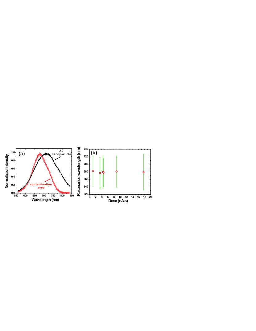
Figure 2(b) shows an additional scattering event from an entity at the bottom of the hyperspectral image. This signal originates from the surface contamination that is formed when the bare substrate is irradiated under the same dose setting as the nanoparticles. Interestingly, the light scattered from this area presents a resonance-like shape as shown in Fig. 3(a). The spectra resembles that of a plasmonic response of an unexposed reference nanoparticle. We find that peak wavelength of the the contamination dots does not significantly depend on as illustrated in Fig. 3(b). The spectral position of the scattering maximum is constant with doses. The error bars represent the full-width at half maximum of the measured spectra. Since the scattering response of the contamination dot is dispersive, the spectrum measured from an irradiated nanoparticle must therefore include a linear combination of the nanoparticle’s response and that of the carbon residue.
IV Effect of electron irradiation
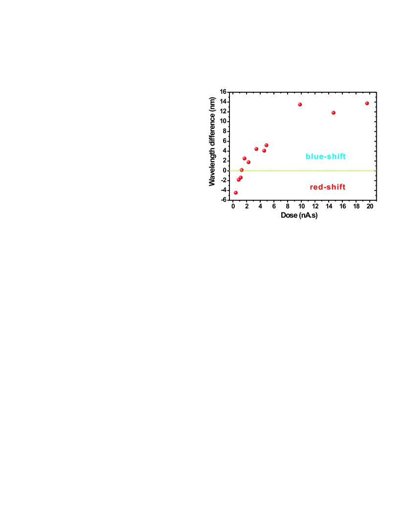
The difference of the resonance wavelength for each Au nanoparticle before and after electron irradiation is analyzed by performing a Gaussian fitting procedure on each spectrum. The resonance wavelength of the pristine particles is obtained by taking the average spectra of the 9 nanoparticles forming the same row, including the reference system. The resonance wavelength of the nanoparticles after contamination is obtained by averaging the scattered peaks of the 8 nanoparticles that were exposed to the electron beam. The wavelength difference before and after electron contamination is thus defined as . The results are plotted as a function of exposure dose in Fig. 4. indicates a redshift of the resonance after exposure compared to the reference spectrum while a positive signifies a blue-shift of the response. For the smallest exposure dose, the resonance wavelength of Au nanoparticles has redshifted compared to the reference nanoparticle as expected from the adhesion of surface adsorbates Kelly03 ; mcfarland03 . For increasing values of , we however systematically observe a shift of the resonances toward the blue part of the spectrum. After =2 nA.s, the spectral maximum is even blue-shifted compared to the reference spectrum as indicated by the positive value of . This blue-shift steadily increases before saturating at 13 nm for doses higher than 10 nA.s.
V Discussion
In order to explain the evolution of with , we fabricated an array of Au nanoparticles and imaged the nanoparticles before and after electron-beam irradiation by SEM without conducting the spectroscopy of section III. We show in Fig. 5 (a) and (b) SEM images of four Au nanoparticles taken before and after electron beam exposure. The lower pair in Fig. 5 (b) is irradiated with a dose =13.2 nA.s and the upper pair with = 17.7 nA.s. Under these doses, the SEM images reveal the appearance of small depressions surrounding the nanoparticles as indicated by the arrows in Fig. 5 (b). The size and depth of the depressions increase with as indicated by the contrast difference of the hollows around the lower and upper pairs. Deformation of the surface resulting from the impact of an electron beam has been reported for various class of materials ranging from III-V compounds, oxides and polymers Ogawa99 ; storm05 ; akiba10 and is generally understood as a strain relaxation of the surface irradiated. A close up view of one irradiated Au nanoparticle with a depression around is shown in Fig. 5(c). In Fig. 5(d), the depression site formed by parking the electron beam on the bare substrate is readily observed 2.5m at the right of the nanoparticle (arrow). At this location, the substrate was exposed under the electron beam with the same dose as on the nanoparticle on the left. It is clear that under a high exposure dose, the carbon contamination induced by the electron beam is etched away knowles07 and the impact of the electron beam leads to a morphological change of the substrate surface. We thus study the cross-over dose for which the surface plasmon response of the Au nanoparticles is affected by a carbonization of its surface or by a local change of the substrate topology.

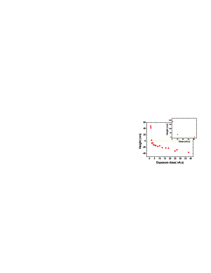
Figure 6(a) shows a three-dimensional rendering of an atomic force microscope (AFM) image of a 12m 12m area of a pristine ITO-covered substrate. The zone was exposed locally to the electron beam using an array of doses. was changed from 1.38 nA.s to 38.1 nA.s. The exposure dose is marked on the top of each parking position. For the lowest exposure dose (=1.38 nA.s and 1.5 nA.s) carbon tips are formed (third line from the top). The growth of these protrusions are fairly reproducible as shown by the array depicted in the SEM image of Fig. 6(b). Here a series of carbon contamination dots formed with =1.38 nA.s and =1.5 nA.s emphasizes the robustness of the contamination. The carbon dots formed with an exposure dose of 1.5 nA.s are slightly larger than those formed at =1.38 nA.s.

When increases to 2.19 nA.s, a small protrusion remains visible in the AFM image of Fig. 6(a). At the next dose, however (=2.43 nA.s) a depression is replacing the contamination dot as indicated by the contrast reversal of the image. Figure 7 displays the height of the carbon tips and the depressions extracted from Fig. 6(a). As the exposure dose increases, the height of the contamination dots decreases and starts to form depressions at around =2.5 nA.s. Within the experimental errors, this dose threshold coincides approximately to the dose for which =0 (Fig. 4). For higher value of , the depression becomes deeper as the exposure dose increases and tends to saturate after 10 nA.s, a value consistent with the saturation of in Fig. 4. Transition from carbon growth on the exposed area to a volatilization of the residues originates from the relative efficiencies of the deposition and etch processes knowles07 . Growth is more efficient but saturates at high beam current to the limited arrival of hydrocarbon species. Conversely, the etching process is less efficient but benefits from the large supply of water molecules present on the substrate and in the chamber.
From the above considerations, we can then conclude that when the exposure dose is small, carbon contamination tips formed on the top surface of the Au particle introduce a small but measurable red-shift of the plasmon resonance. The redshift results from a modified electrical environment attributed to the hydrocarbon adsorbate. As the exposure dose increases, the electron beam is no longer depositing carbon residues and contributes to the desorption of the contamination. At approximately 2.5 nA.s, the position of the resonance shows that the nanoparticle before and after electron-beam exposure is the same. This is confirmed by the vanishing height of the contamination dot. Hence, this exposure dose defines the optimal imaging condition for observing plasmonic nanoparticles without altering their spectroscopic properties. For larger exposure, the geometry of the interface is changed to a concave surface. The blue-shift of the resonance is therefore understood as joint effects arising from a linear combination of the scattering response of the indentation convoluted with that of the nanoparticle, and a modified interface from a planar surface to a concave geometry. We ruled out an irreversible change of the nanoparticle morphology resulting from the repeated impact of the electrons to explain the wavelength shift of the resonance. Under the operating condition of the SEM, the electron-induced temperature rise remains far below the melting temperature of the nanoparticle Reimer ; Borel76 and sputtering of metals is unlikely in a 20 KV SEM Egerton .
We verified that the general trend observed in Fig. 7 is not typical from the instrument used in this study and can be generalized to other SEMs. To this purpose we measured the height of carbon dots on a pristine ITO with a Raith microscope (Pioneer) operating at 20 KV under three different doses. Results are shown in the inset of Fig. 7. The trend is qualitatively reproduced with this microscope, however, carbon growth is inhibited for a larger dose ( 40 nA.s) compared to Fig. 7. While the overall growth and etch processes of the carbon residues are consistent between instruments, the specific dose for which the surface plasmon resonance is unaffected by the electron flux needs to be predetermined for each SEM.
VI Conclusion
We have studied the effect of an electron-beam exposure on the response of plasmonic nanoparticles upon imaging with a SEM. The spectra obtained for Au nanoparticles before and after irradiation indicate the presence of carbon contamination on the surface of the nanoparticle for smaller exposure doses. When the exposure dose increases, AFM and SEM imaging demonstrate that the carbon deposits are etch away and the substrate around Au particles is deformed by the electron beam to form a depression. Under these exposure conditions, the surface plasmon resonance of the nanoparticle systematically blue-shifts passing by its original value before electron beam exposure. An optimum dose can therefore be determined to safely image plasmonic nanostructures with SEM without altering their spectroscopic response.
VII Acknowledgements
The research leading to these results has received funding from the European Research Council under the European Community’s Seventh Framework Program FP7/2007-2013 Grant Agreement no 306772. This project is in cooperation with the regional council of Burgundy under PARI SMT3 and the Labex ACTION program (contract ANR-11-LABX-01-01). M. S. acknowledges the support of the Jiangsu Specially-Appointed Professor Program (R2012T01) and the Foundation for special project on the Integration of Industry, Education and Research of Jiangsu Province (BY2012028).
References
- (1) M.E. Stewart, L.B. Anderton, Christopher R.and Thompson, J. Maria, S.K. Gray, J.A. Rogers, R.G. Nuzzo, Chem. Rev. 108, 494 (2008)
- (2) K.M. Mayer, J.H. Hafner, Chem. Rev. 111(6), 3828 (2011)
- (3) N.J. Halas, S. Lal, W.S. Chang, S. Link, P. Nordlander, Chem. Rev. 111(6), 3913 (2011)
- (4) S.S. Aćimović, M.P. Kreuzer, M.U. González, R. Quidant, ACS Nano 3(5), 1231 (2009)
- (5) K.M. Mayer, F. Hao, S. Lee, P. Nordlander, J.H. Hafner, Nanotech. 21(25), 255503 (2010)
- (6) P. Zijlstra, M. Paulo, Pedro M. R.and Orrit, Nature Nanotech. 7, 379 (2012)
- (7) I. Ament, J. Prasad, A. Henkel, S. Schmachtel, C. Sönnichsen, Nano Lett. 12(2), 1092 (2012)
- (8) M. Hu, C. Novo, A. Funston, H. Wang, H. Staleva, S. Zou, P. Mulvaney, Y. Xia, G.V. Hartland, J. Mater. Chem. 18, 1949 (2008)
- (9) N. Liu, M. Hentschel, T. Weiss, A.P. Alivisatos, H. Giessen, Science 332(6036), 1407 (2011)
- (10) J. Margueritat, H. Gehan, J. Grand, G. Lévi, J. Aubard, N. Félidj, A. Bouhelier, G. Colas-Des-Francs, L. Markey, C. Marco De Lucas, A. Dereux, E. Finot, ACS Nano 5(3), 1630 (2011)
- (11) W.S. Chang, J.B. Lassiter, P. Swanglap, H. Sobhani, S. Khatua, P. Nordlander, N.J. Halas, S. Link, Nano Lett. 12(9), 4977 (2012)
- (12) T.K. Sau, A.L. Rogach (eds.), Complex-Shaped Metal Nanoparticles: Bottom-Up Syntheses and Applications (Wiley-VCH Verlag GmbH & Co, 2012)
- (13) T.C. Isabell, P.E. Fischione, C. O’Keefe, M.U. Guruz, V.P. Dravid, Microsc. Microanal. 5, 126 (1999)
- (14) S.Graells, S Aćimovíc, G. Volpe and R. Quidant; Plasmo. 5, 135 (2010)
- (15) K.I. Schiffmann, Nanotech. 4(3), 163 (1993)
- (16) M. Antognozzi, A. Sentimenti, U. Valdrè, Microsc. Microanal. Microstruct. 8(6), 355 (1997)
- (17) S. Johnson, D. Hasko, K. Teo, W. Milne, H. Ahmed, Microelectr. Eng. 61–62(0), 665 (2002)
- (18) T. Djenizian, L. Santinacci, H. Hildebrand, P. Schmuki, Surf. Sci. 524(1–3), 40 (2003)
- (19) A.J.V. Griffiths, T. Walther, J. Phys.: Conference Series 241(1), 012017 (2010)
- (20) M. Toth, C.J. Lobo, M.J. Lysaght, A.E. Vladár, M.T. Postek, J. Appl. Phys. 106(3), 034306 (2009)
- (21) S. Horiuchi, T. Hanada, M. Ebisawa, in EMC 2008 14th European Microscopy Congress 1–5 September 2008, Aachen, Germany, ed. by M. Luysberg, K. Tillmann, T. Weirich (Springer Berlin Heidelberg, 2008), pp. 387–388
- (22) C.G. Morgan, R. Vane, in Proc. SPIE, Metrology, Inspection, and Process Control for Microlithography XXVI, vol. 8324, ed. by A.Starikov (2012)
- (23) J. Mock, M. Barbic, D.R. Smith, D.A. Schultz, S. Schultz, J. Chem. Phys 116, 6755 (2002)
- (24) A. Bouhelier, R. Bachelot, J. Im, G.P. Wiederrecht, G. Lerondel, S. Kostcheev, P. Royer, J. Phys. Chem. B 109, 3195 (2005)
- (25) K.L. Kelly, E. Coronado, L.L. Zhao, G.C. Schatz, J. Phys. Chem. B 107(3), 668 (2003)
- (26) A.D. McFarland, R.P. Van Duyne, Nano Letters 3(8), 1057 (2003)
- (27) T. Ogawa, M. Akabori, J. Motohisa, T. Fukui, Phys. B: Cond. Mat. 270(3–4), 313 (1999)
- (28) A.J. Storm, J.H. Chen, X.S. Ling, H.W. Zandbergen, C. Dekker, J. Appl. Phys. 98(1), 014307 (2005)
- (29) M. Kotera, Y. Akiba, Jap. J. Appl. Phys. 49(6), 06GE08 (2010)
- (30) M. Toth, C. J. Lobo, G. Hartigan, and W. R. Knowles, J. Appl. Phys. 101, 054309 (2007)
- (31) L. Reimer, Scanning Electron Microscopy: Physics of Image Formation and Microanalysis (Springer Series in Optical Sciences, 1998)
- (32) Ph. Buffat and J-P. Borel, Phys. Rev. A 13(6), 2287 (1976)
- (33) R.F. Egerton, P. Li, and M. Malac, Micron 35, 399 (2004)