High optical efficiency and photon noise limited sensitivity of microwave kinetic inductance detectors using phase readout.
Abstract
We demonstrate photon noise limited performance in both phase and amplitude readout in microwave kinetic inductance detectors (MKIDs) consisting of NbTiN and Al, down to 100 fW of optical power. We simulate the far field beam pattern of the lens-antenna system used to couple radiation into the MKID and derive an aperture efficiency of 75%. This is close to the theoretical maximum of 80% for a single-moded detector. The beam patterns are verified by a detailed analysis of the optical coupling within our measurement setup.
In the next decades millimeter and sub-mm astronomy requireScott et al. (2010) large format imaging arrays to complement the high spatial resolution of the Atacama Large Millimeter/submillimeter ArrayBrown, Wild, and Cunningham (2004). The desired sensors should have a background limited sensitivity and a high optical efficiency and enable arrays of up to megapixels in size. The most promising candidate to fulfill these requirements are microwave kinetic inductance detectors (MKIDs)Day et al. (2003) due to their inherent potential for frequency domain multiplexing. MKIDs are superconducting resonators, thousands of which can be coupled to a single feedline. Each resonator is sensitive to changes in the Cooper pair density induced by absorption of sub-mm radiation. By monitoring the change in either phase or amplitude of the complex feedline transmission at the MKID resonance one can measure the absorbed photon power. Using amplitude readout photon noise limited performance has been shownYates et al. (2011). However, for practical applications two key properties need to be demonstrated: (1) Photon noise limited operation in phase readout. (2) A measurement of the aperture efficiencyRohlfs and Wilson (2004), which describes the absolute optical coupling of a MKID imaging array to a plane wave.
In this letter we present antenna coupled hybrid NbTiN-Al MKIDs designed for groundbased sub-mm astronomy. We show that these devices achieve photon noise limited performance in both amplitude and phase readout. Through a detailed analysis of the optical coupling within our setup we validate the simulation of the lens-antenna far field beam pattern. From this we derive an aperture efficiency of 75%. This is close to the theoretical maximum of 80% for a single-moded detector.
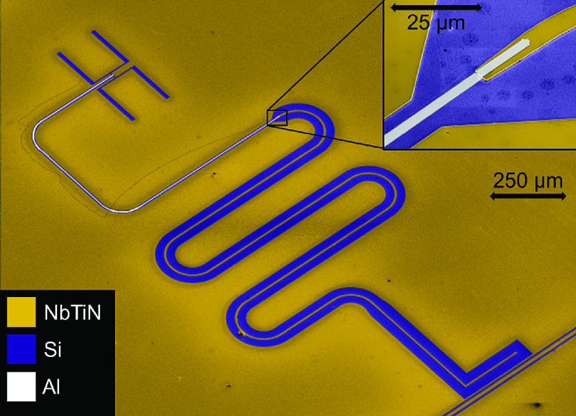
The device design, shown in Fig. 1, aims to simultaneously maximize the phase response and minimize the two-level system (TLS) noise contributionGao et al. (2007). The device is a mm long quarter wavelength coplanar waveguide (CPW) resonator consisting of two sections. The first section ( mm), at the open end of the resonator, is a wide CPW made entirely from 200 nm thick NbTiN. NbTiN has 10 dB lower TLS noise than conventional superconductors such as AlBarends et al. (2009). The TLS noise is further reduced by the width of the CPWBarends et al. (2009), 23.7 and 5.4 for the CPW gap and central line, respectively.
The second section (1 mm), at the shorted end of the resonator, is a narrow CPW with NbTiN groundplanes and a 48 nm thick Al central line. The Al is galvanically connected to the NbTiN central line (Fig. 1 inset) and the NbTiN groundplane at the resonator short. The NbTiN is lossless for frequencies up to the gap THz ( K). Any radiation with a frequency THz is therefore absorbed in the Al ( K) central line of the second section. The optically excited quasiparticles are trapped in the Al, because it is connected to a high gap superconductor. This quantum well structure confines the quasiparticles in the most responsive part of the MKID and allows us to maximize the response by minimizing this active volume. Therefore, we use a narrow CPW in section two, 2.3 and 3.7 for the central line and slots, respectively. Using a narrow Al line at the shorted end of the MKID does not increase the TLS noise significantly, because of the negligible electric field strength in this part of the detector.
At the shorted end of the resonator light is coupled into the device through a single polarization twin-slot antenna, which is optimized for GHz. The advantage of using antenna coupling is that it can be designed independently from the distributed CPW resonator. The disadvantage is that the antenna occupies only of the total pixel footprint. To achieve a high filling fraction we use elliptical lenses to focus the light on the antennas.
The design presented here is an improvement on that by Yates et.al.Yates et al. (2011). Our design has a wider body in section one, which provides dB reduction of the TLS noise. In addition we have thinner Al, 48nm instead of 80 nm. This increases the kinetic inductance fraction by 45% to and reduces the volume by 40%. Both give a linear increase in the phase response.
An array of 24 pixels has been fabricatedLankwarden et al. (2012); Air on a high resistivity ( ) -oriented Si substrate. All pixels are capacitively coupled to a single feedline with a coupling , which is matched to the expected for an optical loading of pW. After mounting an array of 16 laser machined Si lenses with a diameter of 2 mm on the central pixels, the array is evaluated using a pulse tube pre-cooled adiabatic demagnetization refrigerator with a box-in-a-box cold stage designBaselmans et al. (2012). In this design the array is fully enclosed in a 100 mK environment with the exception of a 2 mm aperture, which is located 15.05 mm above the approximate center of the MKID array. This aperture is isotropically illuminated by a large temperature-controlled blackbodyde Visser et al. (2013). Two metal mesh filters provide a minimum rejection of 20 dB at all wavelengths outside the 50 GHz bandpass centered on GHz. This allows us to create a variable unpolarized illumination over a wide range of powers.
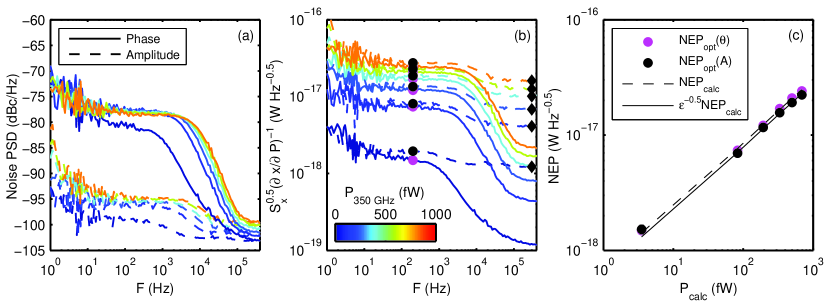
Fig. 2(a) shows the amplitude and phase noise spectra measured for a typical device as a function of the optical power absorbed in the Al, . In this figure we observe two characteristics that prove our device is photon noise limited:
-
1.
The noise spectra in both phase and amplitude are white with a roll-off given by the quasiparticle lifetime, , or resonator ring time, . For our devices we observe a white noise spectrum for fW, which has a roll-off due to , because .
-
2.
When reducing the optical loading from the photon noise limited situation one should observe at negligible power levels the transition to a noise spectrum that is limited by intrinsic noise sources of the detector. At a negligible optical loading ( fW) the phase noise spectrum is no longer white and the noise level in both phase and amplitude readout is lower with respect to fW.
Fig. 2 shows three more features, which may be present in a photon noise limited MKID.
The photon noise level of the spectra observed in Fig. 2(a) is independent of the optical loading, because the product of quasiparticle number and quasiparticle lifetime is constantBaselmans (2012); de Visser et al. (2013) and the loaded Q did not change.
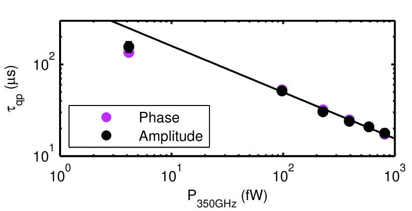
By fitting a lorentzian roll-offde Visser et al. (2013) to the spectra presented in Fig. 2(a) we derive the quasiparticle lifetime as a function of the optical loading. Fig. 3 shows that the quasiparticle lifetime obtained from phase and amplitude readout is equal for all loading levels. For fW the quasiparticle lifetimes show a relation, which matches the expected relationBaselmans (2012); Bardeen, Cooper, and Schrieffer (1957); Kaplan et al. (1976) for a homogeneously illuminated superconductor. At fW we observe , which deviates from the trend set by the photon noise limited regime and is significantly lower than the ms observed by de Visser et.al.de Visser et al. (2011) in similar Al. Measurements on hybrid NbTiN-Al MKIDs with a varying length of the Al section show that the quasiparticle lifetime increases with the Al length. Based on this we tentatively conclude that the reduced lifetime we observe is due to poisoning by quasiparticles entering from the NbTiN.
Fig. 2(b) and 2(c) show the observed Noise Equivalent Power (NEP)de Visser et al. (2013); Tim , the level of which only depends on the optical loading and is thus equal in amplitude and phase readout. The NEP follows the relation expected for photon noise limited MKIDsYates et al. (2011); Baselmans (2012); NEP .
Given the equal NEP values, Fig. 2(a) shows why phase readout is preferred for practical background limited systems. The photon noise level in phase readout is 16 dB higher than that in amplitude readout, thereby relaxing the dynamic range requirements of the readout electronics. We estimateKester (2005); Boyd (1986) that with a state-of-the-art readout system based upon the E2V EV10AQ190 analog-to-digital converter (ADC) we can simultaneously read out approximately 1800 of the presented NbTiN-Al MKIDs in phase readout if we accept a 10% degradation of observing time due to the noise added by the ADC alone. Using the same electronics amplitude readout would only allow 30 pixels.
In the photon noise limited regime it is favorable to have a high optical or aperture efficiencyRohlfs and Wilson (2004), , because the observation time required to achieve a given signal-to-noise follows . The most reliable way to determine the aperture efficiency of a MKID is through the measurement of the photon noise. Yates et.al.Yates et al. (2011) used this approach and determined the aperture efficiency by comparing the measured NEP to the NEP expected for a perfect absorber with the same area as a single pixel. The latter was determined using the geometrical throughput between the detector and the illuminating aperture. However, this approach is only valid if the gain of the antenna is equal to its maximum value within the entire angle spanned by the aperture.
We determine the aperture efficiency from the full far field beam pattern, which is obtained from a simulation of the complete lens-antenna system using CST Microwave Studio. This gives us the freedom to adjust the design as required and allows a calculation of independent of the measurement setup. However, the simulated beam pattern does require experimental verification. We will first show how we verify the coupling efficiency, , which describes the reflection losses due to mismatches between the antenna and the resonator CPW, and the gain patternGno , , as a function of the angular direction, , from the microlens focus. The gain pattern of our lens-antenna system is shown in Fig. 4(b). After the verification we will use and , which we obtain from CST Microwave Studio, to calculate .
We verify and using the photon noise limited optical NEP, , as the experimental observable. We compare to the photon noise limited NEP we expect, , from the resonator. To calculate we need to know the power coupled to the lens-antenna system, , which is given by
| (1) |
Here is the speed of light, the filter transmission and Planck’s law for a blackbody temperature . The factor takes into account that we receive only a single polarization. The second integral evaluates the solid angle over the aperture area, . The rest of the detector enclosure is a 100 mK absorber that has a negligible emission at 350 GHz. Included in this calculation is the experimentally measured lateral shift between each pixel and the aperture. The effect of lateral deviations from co-alignment are shown in Fig. 4(a). The contours in this figure show the predicted reduction in received power as a function of the lateral translation between the lenses’ optical axis and aperture center. The contours are normalized to a co-aligned system. The circles in Fig. 4 indicate the positions of the 16 lensed pixels. The color indicates the relative frequency change between 5 and 90 fW of optical loading, which roughly approximates the relative absorbed power for all 16 pixels. The qualitative match is striking and assures us of the shape of .
We can now define the power error ratio as the discrepancy between the calculated and measured photon noise limited NEP.
| (2) | |||||
Here is the photon energy of the incoming radiation, the correction to Poisson statistics due to wave bunchingde Visser et al. (2013), the superconducting energy gap of the absorbing material and the pair breaking efficiency inside this material. is equal to the measured NEP at a modulation frequency of 200 Hz, , after correction for any detector noise contribution to the NEP, . In amplitude readout this is the amplifier noise contribution, which we estimate from the NEP value at a modulation frequency of 300 kHz (black diamonds in Fig. 2(b)). In phase readout as both the frequency independent amplifier noise contribution, observed above the roll-off frequency, and the TLS noise contribution, observed below 10 Hz, are insignificant at 200 Hz. We expect , if the description of the optical power flow is complete and the simulated beam patterns are correct.
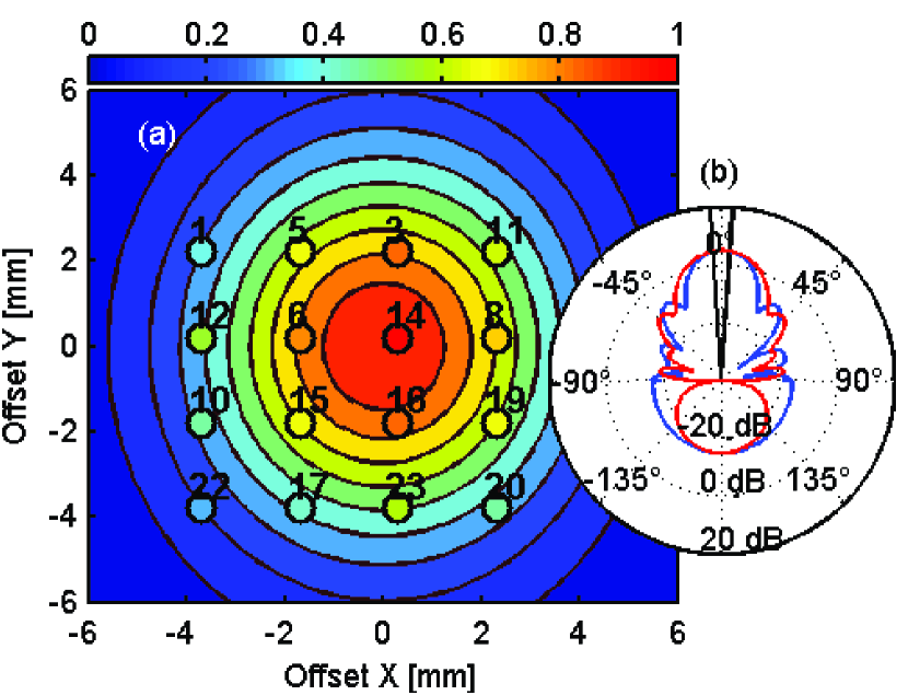
Fig. 2(c) shows the measured optical NEP, , as a function of for phase (magenta dots) and amplitude (black dots) readout. The measured photon noise NEPs from phase and amplitude are within of each other at all loading levels. The solid black line shows the best fit for the expected linear relation, . For the presented MKID, numbered 16, , if we disregard the lowest loading. For a different MKID, numbered 3, the above analysis yields .
From the verified far field beam pattern we can determine , which is mathematically defined as
| (3) |
Here is the physical area covered by the pixel; and are the wavelength and frequency of the observed radiation, respectively; and is the direction of the maximum gain. Using the circular area of the lenses , and the gain of the CST beam pattern at broadside, dB, an aperture efficiency of 75% is determined for a single pixel. The maximum achievable aperture efficiency of a circular antenna illuminated by a single-moded gaussian beam isGoldsmith (1998) . For the measured array the filling fraction of the square packing means we have a total array aperture efficiency of 57%. Using an array with hexagonal packing the total array aperture efficiency can be increased to 66%.
In conclusion, we present hybrid NbTiN-Al MKIDs, which are photon noise limited in both phase and amplitude readout for loading levels fW with an aperture efficiency of 75%. The photon noise level will allow us to simulatenously read out approximately 1800 pixels using state-of-the-art electronics to monitor the phase. Given these specifications, hybrid NbTiN-Al MKIDs should enable astronomically usable kilopixel arrays for sub-mm imaging and moderate resolution spectroscopy.
Acknowledgements.
The authors thank T. Zijlstra, D.J. Thoen and Y.J.Y. Lankwarden for sample fabrication and P.J. de Visser for helpful discussion. T.M. Klapwijk and R.M.J. Janssen are grateful for support from NOVA, the Netherlands Research School for Astronomy, to enable this project. A. Endo is grateful for the financial support by NWO (Veni grant 639.041.023) and the JSPS Fellowship for Research Abroad. The work was in part supported by ERC starting grant ERC-2009-StG Grant 240602 TFPA (A.M. Baryshev). T.M. Klapwijk acknowledges financial support from the Ministry of Science and Education of Russia under contract No. 14.B25.31.0007.References
- Scott et al. (2010) D. Scott, P. Barmby, P. Bastien, J. Cami, E. Chapin, J. Di Francesco, M. Fich, M. Halpern, M. Houde, G. Joncas, D. Johnstone, P. Martin, G. Marsden, B. Matthews, D. Naylor, C. Barth Netterfield, E. Peeters, R. Plume, A. Pope, G. Schieven, T. Webb, and C. Wilson, ArXiv e-prints (2010), arXiv:1008.4159 [astro-ph.IM] .
- Brown, Wild, and Cunningham (2004) R. L. Brown, W. Wild, and C. Cunningham, Advances in Space Research 34, 555 (2004).
- Day et al. (2003) P. K. Day, H. G. LeDuc, B. A. Mazin, A. Vayonakis, and J. Zmuidzinas, Nature 425, 817 (2003).
- Yates et al. (2011) S. J. C. Yates, J. J. A. Baselmans, A. Endo, R. M. J. Janssen, L. Ferrari, P. Diener, and A. Baryshev, Applied Physics Letters 99, 073505 (2011).
- Rohlfs and Wilson (2004) K. Rohlfs and T. L. Wilson, Tools of radio astronomy (Springer, 2004).
- de Visser et al. (2013) P. J. de Visser, J. J. A. Baselmans, J. Bueno, N. Llombart, and T. M. Klapwijk, submitted (2013), arXiv:1306.4238 [cond-mat.supr-con] .
- (7) For clarity the factor is not included .
- Gao et al. (2007) J. Gao, J. Zmuidzinas, B. A. Mazin, H. G. Leduc, and P. K. Day, Applied Physics Letters 90, 102507 (2007), arXiv:cond-mat/0609614 .
- Barends et al. (2009) R. Barends, H. L. Hortensius, T. Zijlstra, J. J. A. Baselmans, S. J. C. Yates, J. R. Gao, and T. M. Klapwijk, IEEE Transactions on Applied Superconductivity 19, 936 (2009).
- Lankwarden et al. (2012) Y. J. Y. Lankwarden, A. Endo, J. J. A. Baselmans, and M. P. Bruijn, Journal of Low Temperature Physics 167, 367 (2012).
- (11) Measurements have shown that the amount of direct absorption by the resonator is negligible when lenses are used. Therefore, we do not use airbridges to connect the groundplanes of the CPW resonator .
- Baselmans et al. (2012) J. J. A. Baselmans, S. J. C. Yates, P. Diener, and P. J. de Visser, Journal of Low Temperature Physics 167, 360 (2012).
- Baselmans (2012) J. J. A. Baselmans, Journal of Low Temperature Physics 167, 292 (2012).
- Bardeen, Cooper, and Schrieffer (1957) J. Bardeen, L. N. Cooper, and J. R. Schrieffer, Physical Review 108, 1175 (1957).
- Kaplan et al. (1976) S. B. Kaplan, C. C. Chi, D. N. Langenberg, J. J. Chang, S. Jafarey, and D. J. Scalapino, Physical Review B 14, 4854 (1976).
- de Visser et al. (2011) P. J. de Visser, J. J. A. Baselmans, P. Diener, S. J. C. Yates, A. Endo, and T. M. Klapwijk, Physical Review Letters 106, 167004 (2011).
- (17) The expected for photon noise limited MKIDs would also be observed for amplifier limited MKIDs, due to the relation. However, in this situation the roll-off in the spectra of Fig. 2(a) would not be observed .
- Kester (2005) W. Kester, The Data Conversion Handbook (Elsevier/Newnes, 2005).
- Boyd (1986) S. Boyd, IEEE Transactions on circuits and systems 33, 1018 (1986).
- (20) We manually normalize the simulated beam pattern to obtain .
- Goldsmith (1998) P. F. Goldsmith, Quasioptical systems : Gaussian beam quasioptical propagation and applications (Wiley - IEEE Press, 1998).