Single-crystal superconducting nanowires of NbSe2 fabricated by reactive plasma etching
Abstract
We present the preparation and measurements of nanowires of single-crystal NbSe2. These nanowires were prepared on ultrathin () flakes of NbSe2 mechanically exfoliated from a bulk single crystal using a process combining electron beam lithography and reactive plasma etching. The electrical contacts to the nanowires were prepared using Ti/Au. Our technique, which overcomes several limitations of methods developed previously for fabricating superconducting nanowires, also allows for the preparation of complex superconducting nanostructures with a desired geometry. Current-voltage characteristics of individual superconducting single-crystal nanowires with widths down to 30 nm and cross-sectional areas as low as 270 nm2 were measured for the first time.
Nanoscale superconductors (wires, disks, loops, etc.) have long been a system of fundamental interest. Investigation of phase slips induced by either thermal activation (TAPS)Arutyunov et al. (2008); Langer and Ambegaokar (1967); McCumber and Halperin (1970); Rogachev et al. (2005); Rogachev and Bezryadin (2003); Tian et al. (2005) or macroscopic quantum tunneling (MQT)Giordano (1988); Lau et al. (2001); Altomare et al. (2006); Bezryadin et al. (2000); Tian et al. (2005) in superconducting nanowires has deepened our understanding of phase coherence at a macroscopic length scale. Work on doubly-connected superconductors, such as ultrathin hollow cylinders of superconductors prepared on an insulating cylindrical substrate – which were shown to exhibit both a destructive regime near half-integer flux quanta,Liu et al. (2001); Wang et al. (2005); Sternfeld et al. (2011) as predicted originally by de Gennes,de Gennes (1981) and a quantum phase transition near the onset of the destructive regimeWang et al. (2005) – has shown that sample topology plays an important role in determining the properties of nanoscale superconductors. The destructive regime is the Little-Parks effectLittle and Parks (1962) in the limit of an ultrasmall cylinder diameter. Furthermore, planar doubly-connected superconducting nanostructures exhibit a Little-Parks-de Gennes effect in which the destructive regime is manipulated through sample geometry by adding a side branch to a superconducting nanoloop.Staley and Liu (2012)
The preparation of nanowires studied previously is usually done by depositing a thin superconducting film on a suitable narrow substrate, resulting in amorphous,Bezryadin et al. (2000); Lau et al. (2001) granular,Rogachev and Bezryadin (2003) or polycrystalline nanowires.Altomare et al. (2005, 2006) Consequently, superconducting weak linksTinkham (1996) may form in the structure, complicating the interpretation of experimental results.Duan (1995) Single-crystal superconducting nanowires can be achieved with molecular beam epitaxy,Guo et al. (2004) but the rapid oxidation of such systems necessitates the addition of a protective capping layer for ex situ transport measurements, which may lead to unintended changes in the device. Single-crystal nanowires can also be prepared by electrochemical deposition in porous media.Tian et al. (2003) However, these wires are difficult to study once released from the porous medium, again because of oxidation. Therefore, the fabrication of ultrathin, single-crystal nanoscale superconductors is of significance.
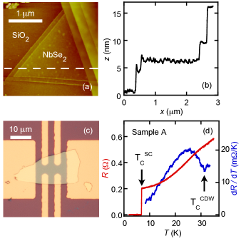
NbSe2 is a layered type-II superconductor, featuring a hexagonal crystal structure with lattice constants of nm and nm.Marezio et al. (1972) Each unit cell consists of two NbSe2 layers in the AB stacking. Bulk NbSe2 has an in-plane coherence length nm and magnetic field penetration depth nm.Sanchez et al. (1995) Using a mechanical exfoliation technique similar to the one developed for graphene, we isolated ultrathin flakes of NbSe2 on a SiO2/Si substrate. The NbSe2 flakes couple to the substrate through a weak van der Waals interaction.Novoselov et al. (2004) Flake thicknesses were determined by means of an atomic force microscope (AFM) calibrated optical color guide, which is accurate to within a single unit cell for flakes with a thickness nm.Staley et al. (2009) AFM scans of typical flakes revealed extended flat terraces, often only nanometers thick, between sharp step edges (Figs. 1(a) and 1(b)).
Conventional photolithography techniques were used to prepare devices of exfoliated NbSe2 flakes (Fig. 1(c)) for the measurement of their electrical transport properties (Fig. 1(d)). All measurements presented in this article were conducted using standard DC techniques in a Physical Property Measurement System with base temperature of K and superconducting magnet capable of fields of T. For the sample shown in Figure 1(c), resistance (R) and dR/dT measurements (Fig. 1(d)) showed a superconducting transition at K and a charge density wave (CDW) transition at K.Inosov et al. (2008) The signature for the CDW transition, an abrupt change of slope in , indicates the high quality of our exfoliated flakes.Iwaya et al. (2003) Magnetoresistance measurements (data not shown) showed the upper critical field, , defined to be the field at which , was T at K with the magnetic field applied along the c axis, yielding an in-plane coherence length of nm, consistent with the bulk value.
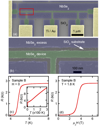
To fabricate a nanowire, large leads for electrical transport measurements were first patterned on the exfoliated flakes using conventional electron beam lithography (EBL). The leads consisted of a nm underlayer of titanium, followed by a nm layer of gold. A second EBL step was used to outline the shape of the device. The entire flake was then subjected to a CF4 reactive ion plasma etch, removing the unprotected NbSe2 and leaving a structure of desired pattern. The plasma etch was performed with a parallel plate system at room temperature at a pressure of Torr with a 200 Volt DC bias and 60 Watt RF power. These parameters yielded an etch rate of Å/s. An acetone bath followed by an O2 plasma etch removed residual EBL resist (the CF4 etch rendered a thin layer of EBL resist insoluble in acetone, necessitating the final O2 etch). Scanning electron microscopy (SEM) imaging demonstrated the good quality of the devices so obtained (Figs. 2(a) and 2(b)). Measurements on Sample B (the rightmost 2 segment in Fig. 2(a)) showed that the nanowire was superconducting with a Tc of 4.8 K (Fig. 2(c)) and critical field of 3.5 T (Fig. 2(d)). The thicknesses of the starting flakes for Samples A and B were different (by at least a factor of 2), leading to different Tc values.Frindt (1972); Staley et al. (2009)
The selective etch process allows for the fabrication of nanostructures of NbSe2 of an arbitrary geometry, including doubly- and multiply-connected samples. Thus, this method has a distinct advantage over existing methods such as templating.Bezryadin et al. (2000) We were able to fabricate independent nanowires from one single-crystal flake, as seen in Figure 2(a), thereby ensuring identical processing conditions among devices.
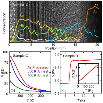
For electrical transport measurements of nanowires, low-resistance contacts are crucial. The contact issue has been the main obstacle for the electrical transport measurements of individual single crystalline nanowires of almost all elemental superconductors.Wang et al. (2004); Tian et al. (2005) In the present case, despite a carefully controlled cleaning process prior to depositing the electrical contacts, low-resistance contacts were difficult to obtain reliably. To gain insight into the behavior of the contact, we performed high resolution cross-sectional transmission electron microscopy (TEM) studies of the interface between the NbSe2 flake and the Ti/Au measurement leads. TEM samples were thinned with a focused beam of gallium ions to allow the transmission of electrons. Due to the destructive nature of the TEM sample preparation, all scans were performed post-measurement. Figure 3(a) shows a TEM image of one contact region of Sample C. The superimposed lines indicate the relative concentrations of elements measured using energy-dispersive x-ray spectroscopy (EDX) with the TEM in scanning mode. Interestingly, Ti was found to diffuse into both the NbSe2 flake and Au overlay. Furthermore, the crystal lattice of the flake abruptly restructures within about 5 nm of the top surface, and the top-most layers of the flake show a pronounced Se deficiency. While the cause of the restructuring of the NbSe2 top layers is not known, it appears to be unrelated to Ti inter diffusion, as the same restructuring was found in portions of flake not covered by Ti. It is possible the restructuring results from a high-vacuum anneal this device was subjected to (discussed below), especially considering the lack of restructuring seen in similar, yet non-annealed, samples. The Se-poor surface region may result from the 180∘C bake all samples were subjected to in order to cure the EBL resist. Interestingly, recent work on ultra-thin exfoliated NbSe2 flakes suggests flakes thinner than 4 unit cells are non-conducting after EBL processing.El-Bana et al. (2013) Prior work utilizing a lithography-free technique, however, observed superconductivity in flakes down to a single unit cell.Staley et al. (2009) It is possible the brief EBL bake causes the Se deficiency and negatively impacts the electrical properties of the topmost layers of material.

Vacuum annealing does seem to improve the contact to our devices. In Figure 3(b), the two-terminal resistance of Sample C reveals insulating behavior over the entire temperature range and a base temperature contact resistance of nearly 100 k. We annealed the device in situ under high vacuum ( Torr), first at 350 K, then at 400 K. The resulting R(T) traces are also shown in Figure 3(b). While annealing does reduce the contact resistance, it may lead to crystal restructuring as pointed out above. Fortunately, as shown in Figure 3(c), low contact resistance can be achieved even without annealing the sample. Here, the three-terminal resistance of another NbSe2 nanowire measured at low temperatures is plotted. After the superconducting drop at K, the residual contact resistance is roughly 900 , which is among the lowest we have measured.
In Figure 4, we show four-terminal current-voltage characteristics with a magnetic field applied along the axis for two nanowires: Sample B of width 90 nm and Sample E of width 30 nm. Both nanowires are 2 m long and 9 nm thick. At low fields, Sample B switches discontinuously between a superconducting state of unmeasurably low resistance and a fully normal resistive state (Fig. 4(a)). At higher fields, where we expect stronger superconducting fluctuations, a finite resistance tail persists at low bias currents. This tail first appears at a field on the same order of magnitude as the one at which Abrikosov vortices are stable in a nanowire of this width.Kogan et al. (2004) However, a comparison with Sample E (Fig. 4(b)) suggests the finite resistance state is not strictly due to Abrikosov vortices – Sample E should be too narrow to sustain vortices, and, furthermore, it exhibits a low bias resistive state even in zero external field. While the resistive tail is also not described satisfactorily by the theory of MQT or TAPS, it may be attributable to other superconducting fluctuations,Larkin and Varlamov (2005) which should be more pronounced in the more geometrically constrained nanowire.
In the high voltage regime, the nanowires exhibit a sharp departure from normal state resistance at a well defined current, (see Fig. 4(c)). The evolution of as a function of applied field is shown in Figure 4(d). The kink in the trace for Sample B may be related to vortex entry,Benkraouda and Clem (1998) especially considering the lack of a corresponding kink for the narrower Sample E. This kink is also absent when the magnetic field is applied in the plane (data not shown). In this orientation, the ratio is comparable to the ratio for Sample E, making vortex entry again unlikely.
The fabrication process we have presented allows for the study of superconductivity in single crystals of arbitrary geometries. While we have achieved low-resistance contacts, the exact mechanism responsible is not well understood. We have utilized this process to investigate nanowires of single-crystal NbSe2, observing a kink in the evolution of the critical current with magnetic field for samples wide enough to allow vortex entry.
The nano fabrication part of this work is supported by the National Science Foundation (NSF) under Grant DMR 0908700 and Penn State MRI Nanofabrication Lab under NSF Cooperative Agreement 0335765, NNIN with Cornell University. The measurement part is carried out using support from the Department of Energy under Grant No. DE-FG02-04ER46159. Y.L. also acknowledges support from NSFC (Grant 11274229) and MOST of China (Grant 2012CB927403).
References
- Arutyunov et al. (2008) K. Y. Arutyunov, D. S. Golubev, and A. D. Zaikin, Phys. Rep.-Rev. Sec. of Phys. Lett. 464, 1 (2008).
- Langer and Ambegaokar (1967) J. Langer and V. Ambegaokar, Phys. Rev. 164, 498 (1967).
- McCumber and Halperin (1970) D. McCumber and B. Halperin, Phys. Rev. B 1, 1054 (1970).
- Rogachev et al. (2005) A. Rogachev, A. Bollinger, and A. Bezryadin, Phys. Rev. Lett. 94, 017004 (2005).
- Rogachev and Bezryadin (2003) A. Rogachev and A. Bezryadin, App. Phys. Lett. 83, 512 (2003).
- Tian et al. (2005) M. Tian, J. Wang, J. S. Kurtz, Y. Liu, M. H. W. Chan, T. S. Mayer, and T. E. Mallouk, Phys. Rev. B 71, 104521 (2005).
- Giordano (1988) N. Giordano, Phys. Rev. Lett. 61, 2137 (1988).
- Lau et al. (2001) C. Lau, N. Markovic, M. Bockrath, A. Bezryadin, and M. Tinkham, Phys. Rev. Lett. 87, 217003 (2001).
- Altomare et al. (2006) F. Altomare, A. M. Chang, M. R. Melloch, Y. Hong, and C. W. Tu, Phys. Rev. Lett. 97, 017001 (2006).
- Bezryadin et al. (2000) A. Bezryadin, C. Lau, and M. Tinkham, Nature 404, 971 (2000).
- Liu et al. (2001) Y. Liu, Y. Zadorozhny, M. M. Rosario, B. Y. Rock, P. T. Carrigan, and H. Wang, Science 294, 2332 (2001).
- Wang et al. (2005) H. Wang, M. M. Rosario, N. A. Kurz, B. Rock, M. Tian, P. Carrigan, and Y. Liu, Phys. Rev. Lett. 95, 197003 (2005).
- Sternfeld et al. (2011) I. Sternfeld, E. Levy, M. Eshkol, A. Tsukernik, M. Karpovski, H. Shtrikman, A. Kretinin, and A. Palevski, Phys. Rev. Lett. 107, 037001 (2011).
- de Gennes (1981) P. G. de Gennes, C. R. Acad. Sci. Ser. II 292, 279 (1981).
- Little and Parks (1962) W. Little and R. Parks, Phys. Rev. Lett. 9, 9 (1962).
- Staley and Liu (2012) N. E. Staley and Y. Liu, Proc. Natl. Acad. Sci. 109, 14819 (2012).
- Altomare et al. (2005) F. Altomare, A. M. Chang, M. R. Melloch, Y. Hong, and C. W. Tu, App. Phys. Lett. 86, 172501 (2005).
- Tinkham (1996) M. Tinkham, Introduction to Superconductivity (McGraw-Hill, New York, 1996).
- Duan (1995) J.-M. Duan, Phys. Rev. Lett. 74, 5128 (1995).
- Guo et al. (2004) Y. Guo, Y. Zhang, X. Bao, T. Han, Z. Tang, L. Zhang, W. Zhu, E. Wang, Q. Niu, Z. Qiu, et al., Science 306, 1915 (2004).
- Tian et al. (2003) M. Tian, J. Wang, J. S. Kurtz, T. E. Mallouk, and M. H. W. Chan, Nano Lett. 3, 919 (2003).
- Marezio et al. (1972) M. Marezio, A. Menth, G. Hull, and P. Dernier, J. Sol. State Chem. 4, 425 (1972).
- Sanchez et al. (1995) D. Sanchez, A. Junod, J. Muller, H. Berger, and F. Levy, Physica B 204, 167 (1995).
- Novoselov et al. (2004) K. Novoselov, A. Geim, S. Morozov, D. Jiang, Y. Zhang, S. Dubonos, I. Grigorieva, and A. Firsov, Science 306, 666 (2004).
- Staley et al. (2009) N. E. Staley, J. Wu, P. Eklund, Y. Liu, L. Li, and Z. Xu, Phys. Rev. B 80, 184505 (2009).
- Inosov et al. (2008) D. S. Inosov, V. B. Zabolotnyy, D. V. Evtushinsky, A. A. Kordyuk, B. Buechner, R. Follath, H. Berger, and S. V. Borisenko, New J. Phys. 10, 125027 (2008).
- Iwaya et al. (2003) K. Iwaya, T. Hanaguri, A. Koizumi, K. Takaki, A. Maeda, and K. Kitazawa, Physica B 329, 1598 (2003).
- Frindt (1972) R. Frindt, Phys. Rev. Lett. 28, 299 (1972).
- Wang et al. (2004) H. Wang, J. Wang, M. Tian, L. Bell, E. Hutchinson, M. M. Rosario, Y. Liu, A. Amma, and T. Mallouk, App. Phys. Lett. 84, 25 (2004).
- El-Bana et al. (2013) M. S. El-Bana, D. Wolverson, S. Russo, G. Balakrishnan, D. M. Paul, and S. J. Bending, Supercond. Sci. Tech. 26, 125020 (2013).
- Kogan et al. (2004) V. G. Kogan, J. R. Clem, and R. G. Mints, Phys. Rev. B 69, 064516 (2004).
- Larkin and Varlamov (2005) A. Larkin and A. Varlamov, Theory of Fluctuations in Superconductors (Oxford University Press, 2005).
- Benkraouda and Clem (1998) M. Benkraouda and J. R. Clem, Phys. Rev. B 58, 15103 (1998).