Charge transport in InAs nanowire Josephson junctions
Abstract
We present an extensive experimental and theoretical study of the proximity effect in InAs nanowires connected to superconducting electrodes. We fabricated and investigated devices with suspended gate controlled nanowires and non-suspended nanowires, with a broad range of lengths and normal state resistances. We analyze the main features of the current-voltage characteristics: the Josephson current, excess current, and subgap current as functions of length, temperature, magnetic field and gate voltage, and compare them with theory. The Josephson critical current for a short length device, nm, exhibits a record high magnitude of nA at low temperature that comes close to the theoretically expected value. The critical current in all other devices is typically reduced compared to the theoretical values. The excess current is consistent with the normal resistance data and agrees well with the theory. The subgap current shows large number of structures, some of them are identified as subharmonic gap structures generated by Multiple Andreev Reflection. The other structures, detected in both suspended and non-suspended devices, have the form of voltage steps at voltages that are independent of either superconducting gap or length of the wire. By varying the gate voltage in suspended devices we are able to observe a cross over from typical tunneling transport at large negative gate voltage, with suppressed subgap current and negative excess current, to pronounced proximity junction behavior at large positive gate voltage, with enhanced Josephson current and subgap conductance as well as a large positive excess current.
I Introduction
Semiconducting nanowires (NW) have been a focus of intensive research for their potential applications as building blocks in nano-scale devices. Samuelson (2003); Thelander et al. (2006); Li et al. (2006); Dayeh (2010) The nano-scale dimension of the semiconducting nanowires, comparable to the electronic Fermi wave length, also makes them an attractive platform for studying the fundamental phenomena of quantum transport. By tuning the Fermi wavelength by means of electrostatic gates one gets access to such quantum phenomena as conductance quantization, van Weperen et al. (2013); Abay et al. (2013) and quantum interference effects.Jespersen et al. (2009)
Another research interest has been the proximity effect in nanowires induced by connecting them to superconducting electrodes (S).Xiang et al. (2006); Doh et al. (2005) In such devices, S-NW-S, the nanowire serves as a weak link through which a supercurrent can flow due to the presence of the phase difference between the superconducting condensates.Doh et al. (2005); Nilsson et al. (2012); Abay et al. (2012)
Among a variety of nanowires tested in experiments, nanowires of InAs play a central role.Xiang et al. (2006); Nilsson et al. (2012) This is due to their material properties: high electron mobility, low effective mass, and pinning of the Fermi level in the conduction band that permits highly transparent galvanic S-NW contacts. Hybrid devices of InAs nanowires have demonstrated Andreev subgap conductance,Nishio et al. (2011); Doh et al. (2008); Abay et al. (2013) Josephson field effect,Doh et al. (2005); Nilsson et al. (2012) and Cooper-pair beam splitting.Hofstetter et al. (2009) More recently, the nanowire hybrid devices attracted new attention following theoretical predictions of Majorana bound states in NW-S proximity structures.Mourik et al. (2012); Deng et al. (2012); Das et al. (2012)
In spite of intensive research, no systematic investigation of the proximity effect in InAs nanowires has been reported, leaving open important questions about consistency of the observed transport phenomena and theoretical views of the proximity effect.
In this paper, we report on extensive experimental studies of current-voltage characteristics (IVC) of a large variety of hybrid devices made with InAs nanowires connected to aluminum electrodes. These Al-InAs NW-Al devices include suspended and non-suspended nanowires, nanowires with different lengths, and tested at different temperatures, magnetic fields, and gate voltages. We measured the main proximity effect characteristics: Josephson critical current, excess current, and subgap current features, and we make a quantitative comparison with relevant theoretical models.
Our main conclusion is that the most properties of the proximity effect can be qualitatively understood and quantitatively reasonably well fit on the basis of existing theory. In particular, the record high Josephson critical current of 800 nA, observed in the shortest studied nanowire (with 30 nm separation between superconducting electrodes) is close to the theoretical bound for ballistic point contacts.Kulik and Omel’yanchuk (1975) In longer devices, the decay of the critical current with length is consistent with a cross over from ballistic to diffusive transport regime, followed by cross over from a short- to long-junction behavior.
In the gate controlled suspended devices we observe a cross over from a distinct S-normal metal-S (SNS) type behavior with large positive excess current and enhanced subgap conductance to tunneling S-inslulator-S (SIS) type behaviour in accordance with gradual depletion of the conducting channels by the gate potential and increase of the wire resistance.
We also observe subgap current features associated with Multiple Andreev Reflection (MAR) transport.Klapwijk et al. (1982) In addition to those MAR features we systematically observe subgap features, which are not associated with MAR but have some different origin. These features are not related to phonon-induced resonances,Kretinin et al. and they do not seem to have an electromagnetic origin. They appear on the IVCs as voltage steps, strikingly similar to the voltage steps generated by phase slip centers in superconducting whiskers.Meyer and Minnigerode (1972); Skocpol et al. (1974)
The structure of the paper is as follows: After describing the device fabrication and experimental setup in Section II, we summarize the normal state conduction properties of the devices in Section III, which give the necessary input for choosing an appropriate theoretical model of the proximity effect described in Section IV. Then in the following sections we discuss the superconducting transport properties: excess current in Section V, Josephson current in Section VI, sub gap current, and variation of the current under the gate potential in Section VII. Section IX contains conclusive remarks.
II Experimental details
II.1 Sample Fabrication
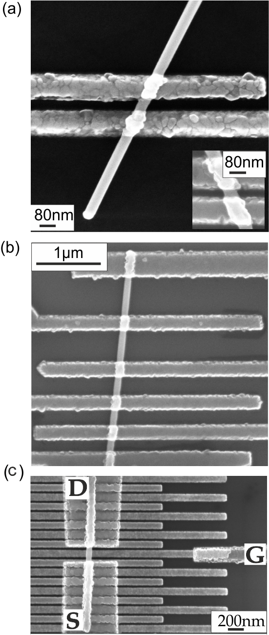
The devices we have investigated are of three types: nanowires placed directly on the substrate with either a) two superconducting contacts or b) multiple contacts, and c) suspended devices with local gates (Fig. 1). All devices are made on standard Si substrates capped by 400 nm thick SiO2.
The nanowires are grown by chemical beam epitaxy.Ohlsson (2002) In the growth process, metal-organic gaseous sources are thermally cracked to their components and the growth materials are directed as a beam towards an InAs substrate placed in the growth chamber. At the optimal temperature, the nanowire growth is catalyzed by Au aerosol particles that have been distributed on the substrate. The sizes of the Au-seeds determine the diameter of the nanowires. In this paper, the nanowires are taken from a single growth batch with an average diameter of nm.
To fabricate the non-suspended devices, InAs nanowires are first transferred to a Si substrate and their relative positions with respect to predefined marks are determined with the help of scanning electron microscope (SEM) images. The extracted locations are then used to pattern superconducting Ti/Al (5/150 nm thick) contacts on top of the nanowires. Depending on the intended device length, i.e. distance between source and drain electrodes, the superconducting contacts are defined by either single-step or double-step electron beam (e-beam) lithography.Abay et al. (2012) The shorter devices ( nm) are defined by the double-step e-beam lithography whereas the longer devices ( nm) are defined by the single-step e-beam lithography. A SEM image of a typical two terminal device ( 100 nm defined by the single e-beam lithography) is shown in Fig. 1a. The inset image shows a short length device of 60 nm defined by the double-step e-beam lithography.
To fabricate the suspended devices, a standard Si substrate is first patterned with interdigitated Ti/Au stripes.Nilsson et al. (2008) InAs nanowires are then transferred to the already patterned Si substrate and some of the nanowires end up on top of the interdigitated metal stripes. The stripes are patterned in a two-step fabrication process in order to get a height difference of 15 nm between every two adjacent stripes. This allows the nanowires to rest on the thicker electrodes (65 nm thick) while being suspended above the substrate and the thinner electrodes (50 nm thick). With the help of SEM images, the positions of suitable nanowires are found and superconducting electrodes Ti/Al (5/150 nm thick) are defined on selected nanowires with e-beam lithography. A SEM image of a suspended device is shown in Fig. 1c.
To get good transparency of the metal-nanowire interfaces, an ammonium polysulfide solution (NH4Sx) cleaning process Suyatin et al. (2007); Abay et al. (2012) has been used prior to evaporation of the superconducting contacts. The samples are then characterized at room temperature and stored in a vacuum box before further measurements at low temperatures.
II.2 Experimental setup
Current-voltage characteristics of the devices are measured in a dilution refrigerator with a base temperature of 15 mK. The IVCs are recorded in either current or voltage bias configuration. In the current-bias mode, the current is determined by a high resistance bias resistor in series with the device. As we increase the current, the voltage across the device is simultaneously measured with a differential amplifier. In the voltage-bias mode, a voltage is directly applied across the device while the current is measured simultaneously by a transimpedance amplifier. To decrease noise coupling to the devices, the electrical lines in the measurement set up are well filtered and thermally anchored at different temperature stages of the refrigerator. The measurement setup is also designed to measure IVCs as a function of temperature and magnetic field.
| Device | L(nm) | Rn(k | Im(nA) | |||
| A | 1 | 30 | 0.16 | 800 | 1.02 | 1.52 |
| 2 | 90 | 0.55 | 95 | 0.40 | 0.87 | |
| 3 | 100 | 0.56 | 54 | 0.23 | 0.75 | |
| 4 | 220 | 1.04 | 30 | 0.24 | 0.76 | |
| B | 5a | 150 | 1.07 | 50 | 0.41 | 1.20 |
| 5b | 170 | 1.28 | 40 | 0.39 | 1.28 | |
| 5c | 180 | 1.34 | 36 | 0.37 | 1.31 | |
| 5d | 190 | 1.37 | 35 | 0.36 | 1.11 | |
| 6a | 110 | 1.84 | 23 | 0.32 | 1.21 | |
| 6b | 200 | 2.40 | 12 | 0.21 | 0.81 | |
| 6c | 250 | 2.72 | 9 | 0.20 | 0.77 | |
| 6d | 500 | 4.21 | 3 | 0.10 | 0.71 | |
| 6e | 600 | 4.82 | 1 | 0.04 | 0.64 | |
| C | 7 | 200 | 2.23 | 15 | 0.24 | 1.30 |
| 8 | 150 | 3.3 | 13 | 0.34 | 1.17 | |
| 9 | 130 | 2.19 | 28 | 0.47 | 1.02 | |
| 10 | 300 | 3.80 | 6 | 0.17 | 1.23 | |
| 11 | 150 | 5.01 | 2.6 | 0.10 | 0.78 | |
| 12 | 200 | 3.6 | 7.5 | 0.21 | 1.11 |
II.3 Current-voltage characteristics
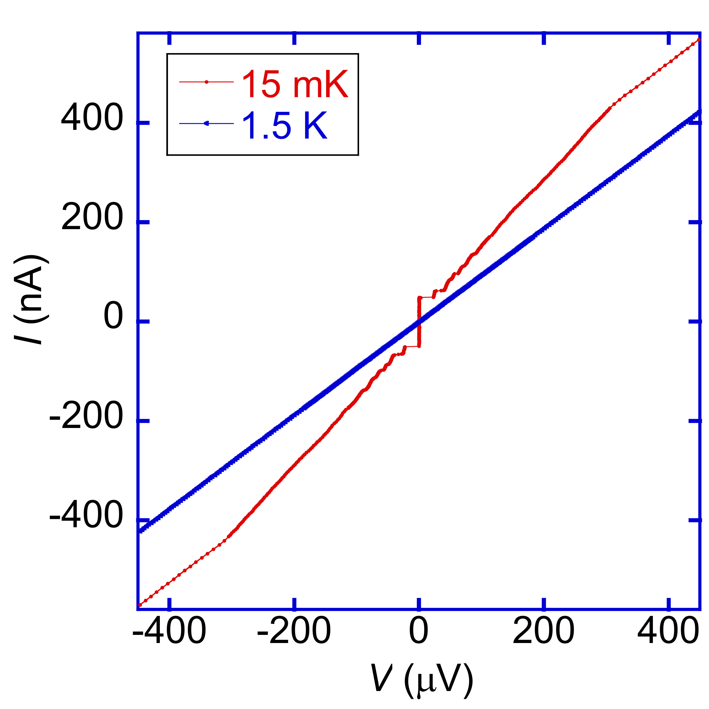
A typical IVC is shown in Fig. 2 for a device of length nm (sample B5a in Table I). Above the critical temperature the IVC (blue) exhibits Ohmic behavior with a normal-state resistance of k. The critical temperature, K, for the devices was determined from samples with shorted electrodes, i.e. without any nanowire. This value agrees well with the temperature at which the Josephson current disappears in the samples with strong Josephson coupling. At temperatures well below , the IVC (red) shows three distinct conductance regimes. i) For voltages , the IVC shows a linear behaviour with the same resistance as in the normal state, . ii) For smaller voltages, , the resistance is approximately and exhibits subgap features. iii) At the zero voltage , the device switches to zero-resistance, exhibiting a Josephson current.
In the next sections we perform quantitative analysis of the IVC, based on a detailed characterization of the normal state current transport in the wire.
III Normal state transport
In order to characterize the normal-state properties of the junctions, dc-measurements have been performed on several devices with a broad range of lengths and resistances. Measurement results for representative devices are sumarized in Table I. The devices are divided into three groups: A, B, and C corresponding to the two-terminal, multi-terminal and suspended devices as shown in Fig. 1.
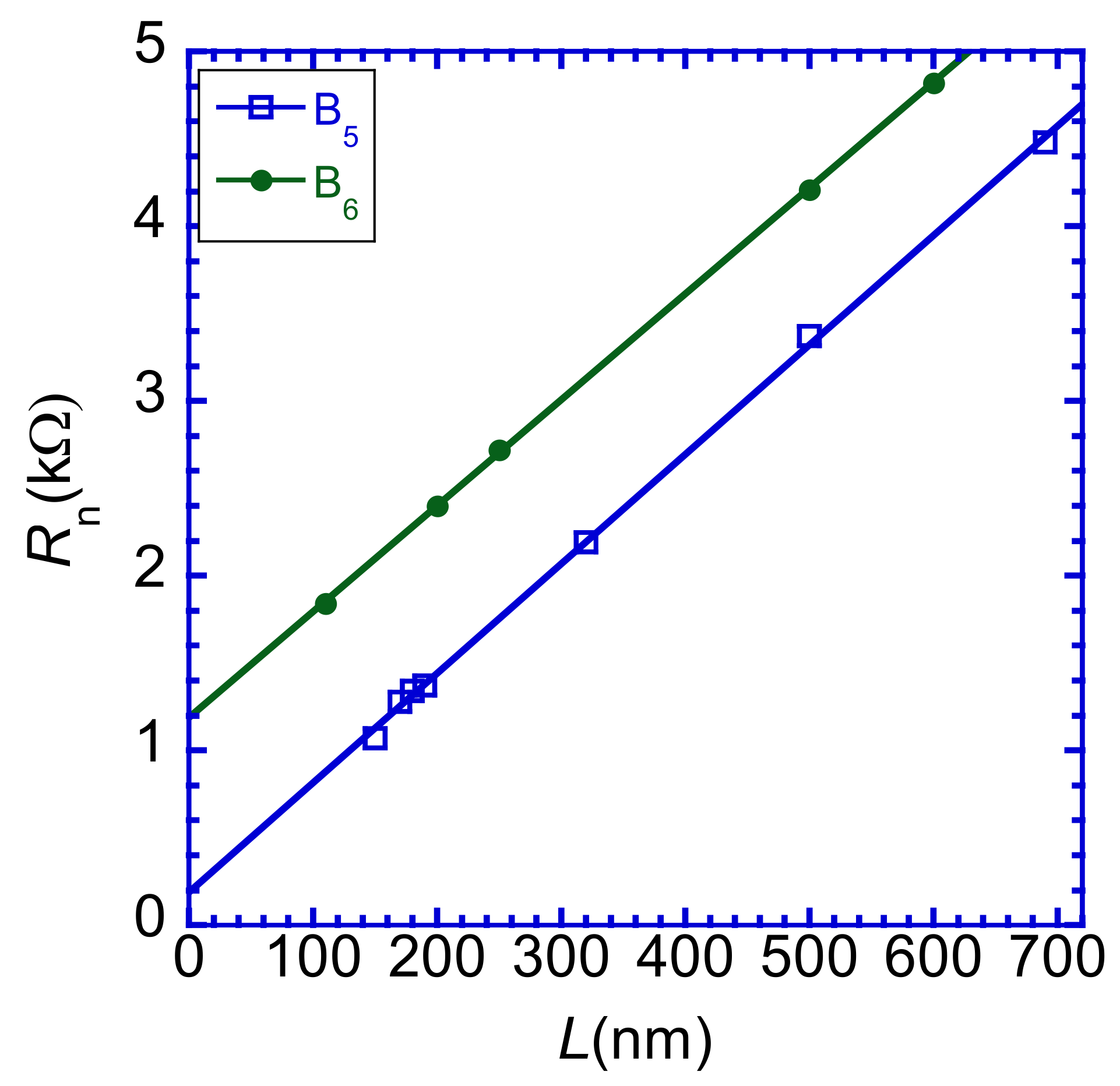
The normal state resistance as a function of length for devices B5 and B6 is plotted in Fig. 3. The resistance of each device increases linearly with length with approximately the same resistance per unit length, /nm. Here, the resistance values are taken from the two-point measurements that also include interface resistance. From the length dependence of the resistance in Fig 3, we extract the contact resistance by extrapolating to zero length. For device B5, we find that contact contribution is less than 180 , while for device B6, it is approximately k.
Taking advantage of multiple contacts of the B type devices we perform two- and four-point measurements of the resistance, which allows us to determine the number of conducting channels and the channel average transparency. The two- and four-point resistance expressions can be written for perfect interfaces as and , respectively,Datta (1997) where is the quantum of resistance, is the number of channels and is the average transparency of the channels. Taking two- and four-point resistance measurements on the same section, we find that our nanowires have a spread in the number of channels ranging between 50 and 100 channels. For instance, for junction B5c, we measured , and , giving the number of channels
| (1) |
This is consistent with the contact resistance found for device B5, and implies perfect S-NW interfaces with transparency close to unity. For the same junction we can then extract the average transparency for the channels.
Assuming only a surface layer of nanowire to be conducting, in analogy with the 2DEG conductivity in planar InAs devices, such a large amount of conducting channels would give unrealistically small value for the Fermi wavelength. On the other hand, assuming the whole bulk of the wire to be conducting we find the electronic Fermi wave length to depend logarithmically on the number of channels, as
| (2) |
This result is arrived at by solving the Schrödinger equation in a cylinder of radius and counting the number of modes (channels) that cross the Fermi level. In Eq. (2) is the -th zero of the -th Bessel function, labels the last mode that contributes to transport. The coefficients and in Eq. (2) are functions of the nanowire radius; for , and , and varying the radius by will change both coefficients approximately by . We can bracket the Fermi wave length between, (100 channels) and (50 channels) for . Our values are consistent with the ones reported for planar InAs 2DEG (), Samuelsson et al. (2004) and for InAs nanowires ().Jespersen et al. (2009) In the further discussions we adopt the values, , and 55 for all the junctions.
| Fermi wavelength | ||
| Fermi wavevector | ||
| Fermi velocity | ||
| Mean free path | ||
| # conducting channels | ||
| Superconducting gap | ||
| Clean coherence length | ||
| Diffusive coherence length | ||
| Diffusion constant | ||
| 12.6 |
Furthermore we use the measured resistance per unit length, /nm, together with the expression for the Drude conductivity, , to evaluate a mean free path for the nanowires of nm. The corresponding Fermi velocity m/s is evaluated by using an electronic effective mass of bulk InAs, where is the free electron mass. The effective mass of electrons for planar InAs 2DEG has been estimated to be in a range from 0.024 to .Samuelsson et al. (2004); Furusaki et al. (1992) The normal state properties of the nanowires are summarized in Table II.
IV Theoretical model
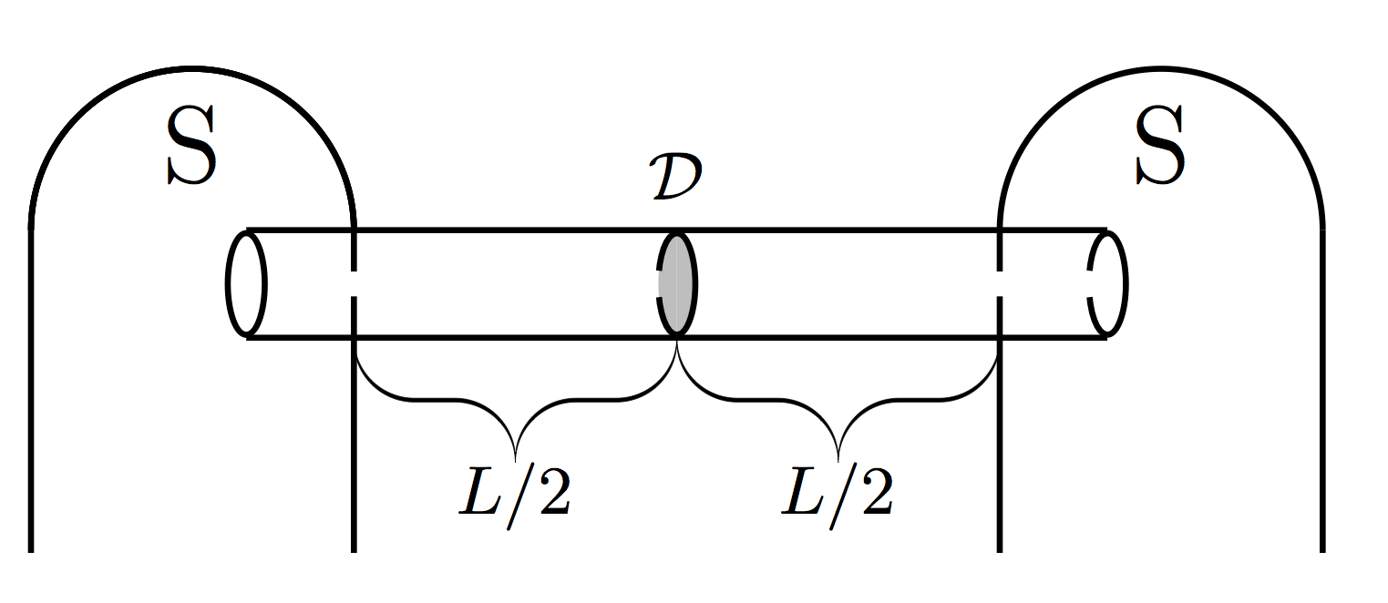
The major difficulty for theoretical interpretation of the experimental data is the very large spread of the wire lengths. Indeed, the shortest wire (30 nm) is in the ballistic point contact regime (, with ), while the longest wire is in the diffusive long junction regime (, with ). The majority of the junctions are in the intermediate cross over region. Furthermore, all the tested junctions exhibit the Josephson effect. This implies that the current transport is fully coherent and requires theoretical modeling within the framework of the coherent MAR theory.Arnold (1987); Bratus’ et al. (1995); Averin and Bardas (1995); Cuevas et al. (1996) To overcome this difficulty, we adopt a simple and tractable model, with which we can bridge between the ballistic and diffusive transport regimes, and describe the cross over to the long junction behavior.com The model setup is shown in Fig. 4. We assume that the two superconducting leads are connected to the nanowire by highly transmissive contacts, which are treated as fully transparent. The nanowire is disordered due to elastic scattering by impurities and crystal imperfections. This is treated in the Born approximation and the mean free path estimated from the experiments infers a scattering rate . Strong defects are included and treated as a single interface having the same effective transparency for all conducting channel. This defect is assumed to be in the centre of the nanowire, and the applied voltage to drop at the defect.
Using the quasi-classical Green’s function methods described in Refs. Cuevas and Fogelström, 2001; Eschrig, 2009, we calculate the IVC as function of device length and transparency by solving the coherent MAR problem. The current is calculated at the scattererCuevas and Fogelström (2001) and expressed through the boundary values, , of the quasi-classical Green’s function for a given channel,
| (3) |
The Green’s function is computed by solving the Eilenberger equation in the right and left parts of the nanowire,
| (4) |
complemented with the Zaitsev boundary conditions at the scatterer and NW-S interfaces.Zaitsev (1984); Cuevas and Fogelström (2001); Eschrig (2009) is the third Pauli matrix in Nambu space. In Eq. (4) we introduce the impurity scattering via the impurity self-energies
| (5) | |||||
| (6) |
is average over directions (). The matrix is the anomalous (off-diagonal) part of the Green’s function . The components of describe the pairing correlations leaking in to the nanowire and two are related by symmetry as .
V Excess current
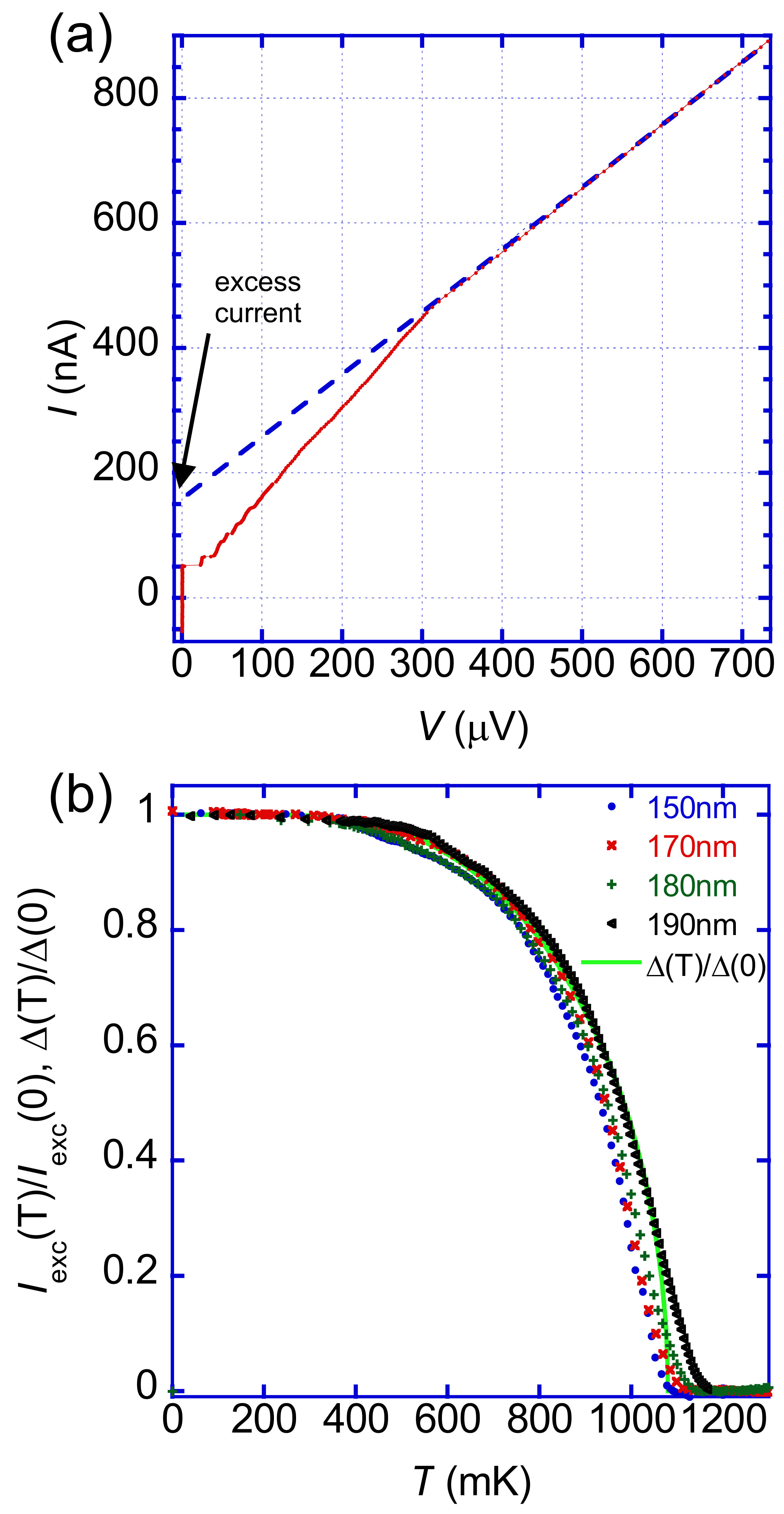
We start with a discussion of the excess current at large voltage, which is a robust feature of the proximity IVC. The excess current, , is extracted from the current-voltage characteristics at large voltage bias using the asymptotic form . The excess current contains contributions both from the single-particle and from the two-particle Andreev currents, and it linearly scales with the energy gap (see e.g. Ref. Shumeiko et al., 1997). In Fig. 5a, the excess current is obtained for the device by extrapolating a linear fit of the IVC measured at (blue dashed line) giving nA. To verify that the measured excess current derives from Andreev scattering processes the experimentally extracted excess current is plotted as a function of temperature in Fig. 5b. As can be seen the amplitude of the excess current follows the temperature dependence of the superconducting gap .
The excess current also depends on the transparency and the length of the nanowire device. In Fig. 6 we present the computed excess current as function of device length together with extracted from the measurements. The maximum values of the theoretical curves correspond to the point contact limit (), and they are in a good agreement with analytical resultsShumeiko et al. (1997), per channel for , and for . When the wire length is increased the excess current decreases. This was also found, experimentally and theoretically, in ballistic 2DEG InAs,Samuelsson et al. (2004), and computed for fully diffusive junctions.Cuevas et al. (2006); Bezuglyi et al. (2011) In our case, the experimental values fall on curves with a typical effective transparency between and being only weakly device dependent between batches of nano wires. These values compare favorably with extracted from the 2-point and 4-point measurements in the normal state.
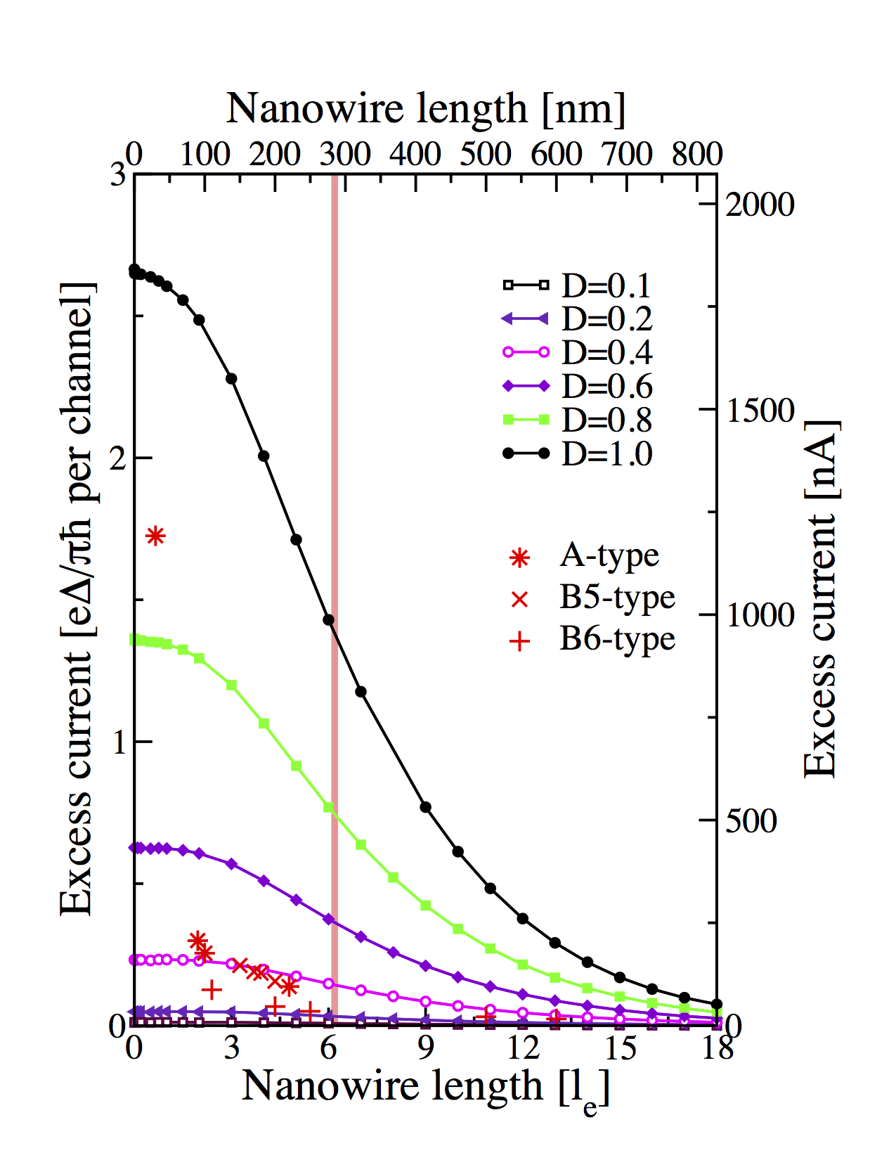
One device, (L=30 nm), however, stands out showing a high transparency of . For this junction, highly transmissive ballistic point contact, one should anticipate the largest critical current.
VI Josephson current
Next, we discuss the Josephson critical current as a function of length, temperature, and magnetic field. The maximum values of the Josephson current, , are extracted from the experimentally obtained IVC at the base temperature of 15 mK and shown in Table I. The maximum currents exhibit a range of values depending on the resistance and length of the devices, from a few nA to 800 nA. Similarly, the characteristic voltage, the -product, also exhibits a range of values, from V to V.
Theoretically, the Josephson current-phase relation is computed using boundary values of the Green’s function, , in Eqs. (3) and (4), the expression reads,Zaitsev (1984)
| (7) |
The sum is over all Matsubara frequencies, , is the temperature, the phase difference over the junction. The critical current is obtained by maximizing the supercurrent.
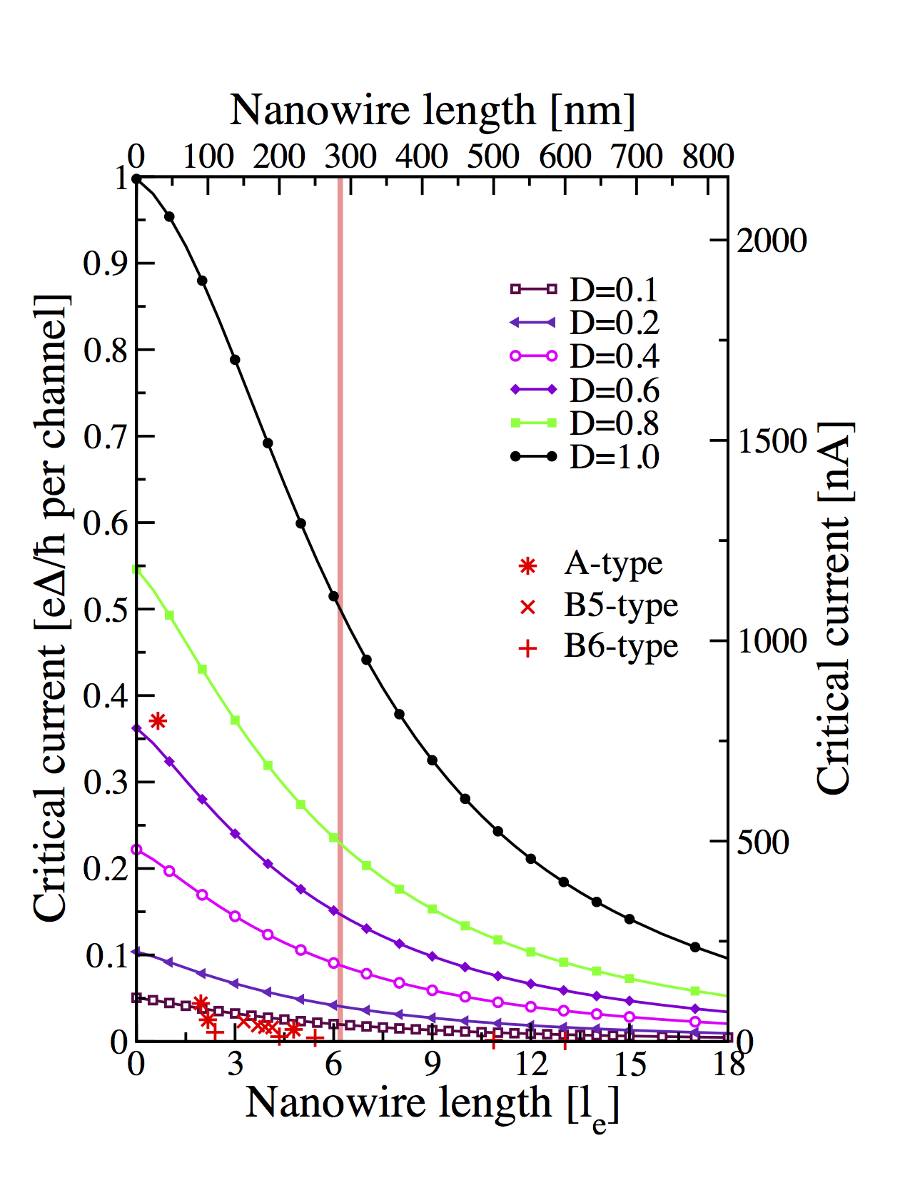
The maximum Josephson currents presented in Table I, together with a theoretical critical current fit, as a function of length, are plotted in Fig. 7. The shortest junction exhibits the largest Josephson current, as expected, with the theoretical fit of the transparency, . This is very close (75%) to the theoretical limit defined by the transparency extracted from the analysis of the excess current. The other junctions fall in the transparency region , which is smaller (approximately by a factor of 4) compared to the transparency extracted from the excess current.
Similar or even larger reduction of Josephson current is commonly observed in nanowires, and it is also common in 2DEG InAs Josephson junctionsSamuelsson et al. (2004). Such an effect is not well understood, perhaps it could be related to some depairing mechanism, for example due to magnetic scattering.
One would expect a certain suppression of the Josephson current extracted from the IVC measurement compared to the equilibrium critical current due to the effect of phase fluctuations. However, our analysis shows that majority of our junctions are overdamped, and the suppression of the critical current in this regime is relatively small and cannot account for the whole suppression effect. Indeed, the capacitances of the devices are estimated in the range, 1-5 fF, cf. Ref. Abay et al., 2012. Assuming fF and the junction resistance, at plasma frequency 1 GHz corresponding to the free space impedance, we estimate the quality factor for the representative junction with critical current, nA. This estimate refers to an unbiased junction, the Q-factor further decreases when the current bias is applied. For such an overdamped regime, , the switching probability is significantly suppressed Martinis and Grabert (1988), and IVC can be modeled with the Ambegaokar-Halperin theory.Ambegaokar and Halperin (1969) This conclusion is supported by the absence of hysteresis on IVC. The IVC measurement takes approximately 1 minute, so that the sample spends approximately few seconds close to Ic. Assuming the temperature of electromagnetic fluctuations being close to the base temperature of 15 mK due to a careful noise filtering,Bladh et al. (2003) we find that the suppression effect accounts for approximately 20% of the theoretical value for the majority of the junctions with critical currents exceeding 10 nA. For the shortest junction with nA the suppression is even smaller, about few percent.
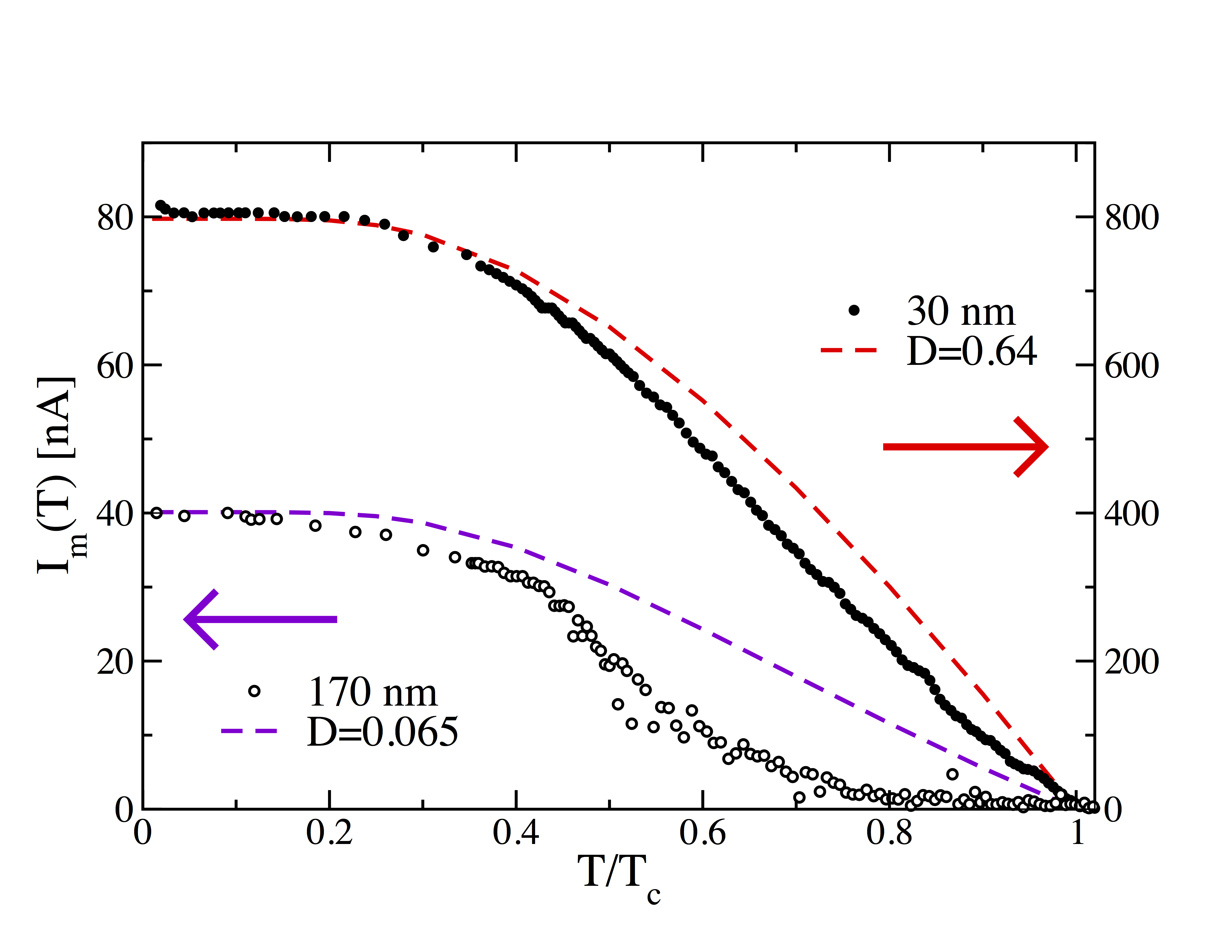
The maximum Josephson current is also investigated as a function of temperature for several devices. The maximum currents for the shortest length device A1 (nm and k), and for the somewhat longer device B5b, (nm and k), are shown in Fig. 8. At the base temperature 15 mK, the devices have maximum Josephson currents of nA and 40 nA, respectively. The data for the shortest device agree well with theory in a broad range of temperatures. The longer device exhibits a concave shaped decay at higher temperatures and deviates from the theoretical fit. Qualitatively similar shape of has been theoretically found for diffusive junctions with highly resistive interfaces (SINIS),Kupriyanov et al. (1999) and explained with enhancement of electron-hole dephasing in the proximity region due to large dwell time. Such an effect is similar to the effect of increasing length of the junction (cf. Ref. Bezuglyi et al., 2011). Given such a similarity we may conclude that although device B5 has transparent S-NW interfaces, the modelKupriyanov et al. (1999) might better capture the effect of the junction length.
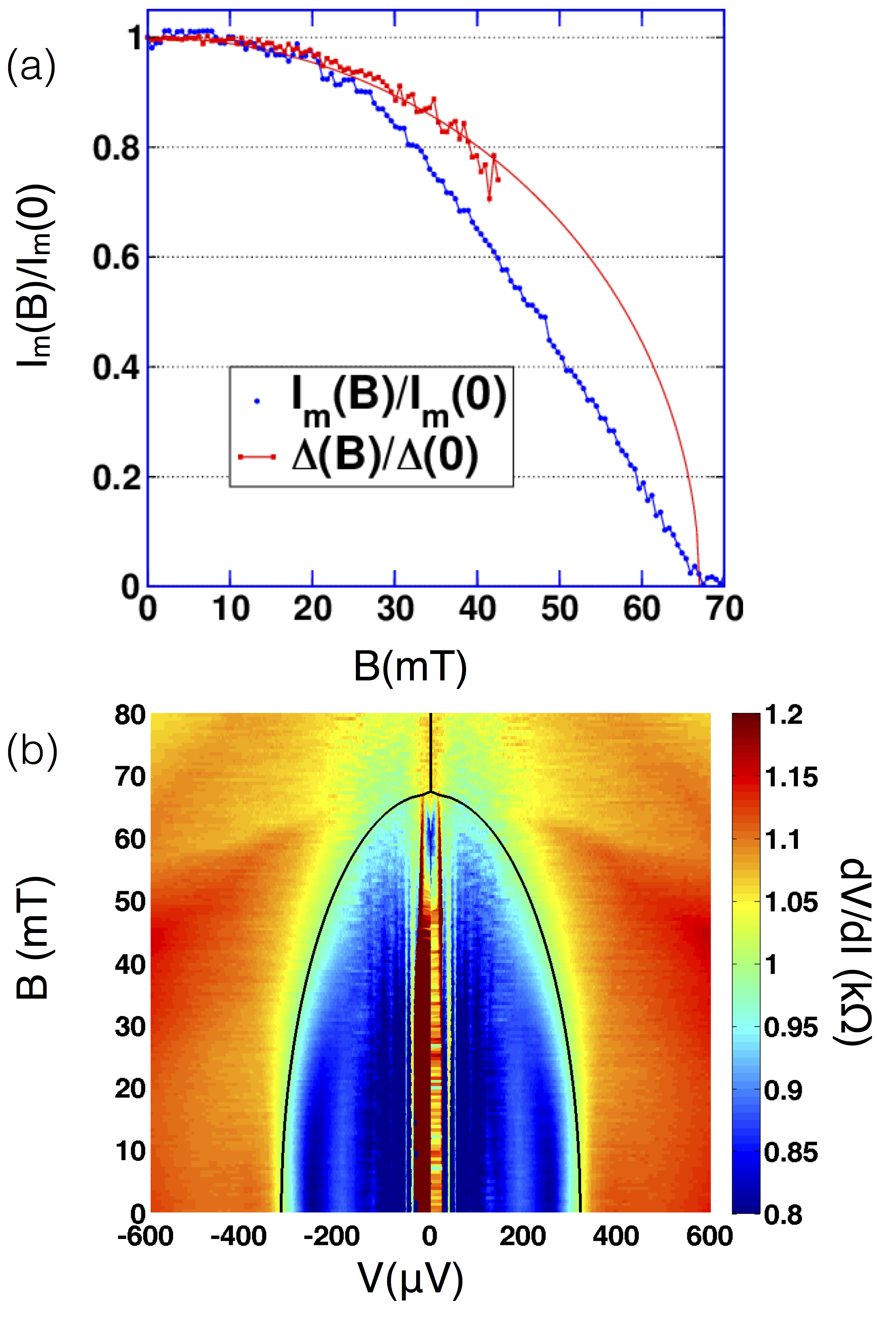
At the base temperature of 15 mK, we also have obtained IVCs as a function of magnetic field. The magnetic field is applied perpendicular to the superconducting leads. The normalized maximum Josephson current and the superconducting energy gap as a function magnetic field are plotted in Fig. 9 for device B5b with nm. The superconducting gap is fitted to the expression from which we extract mT. The maximum current decreases and is totally suppressed above . No Fraunhofer oscillations are observed in any of the devices, consistent with a suppression of superconducting energy gap in the leads.
VII Subgap current
Now we proceed with discussion of the IVC in the subgap region, , as function of temperature and magnetic field, and for different nanowire lengths. A typical plot of the differential resistance as a function of voltage is presented in Fig. 10a. The resistance drops from k at to k at V, which corresponds to the gap value, . Such a drop of resistance in the subgap region is a characteristic of Andreev transport in transmissive SNS junctions.Blonder et al. (1982) Furthermore, the differential resistance shows a second feature at approximately half the gap voltage, V (shown by arrow in Fig. 10a).
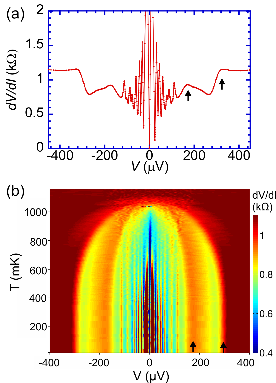
Positions of both these features scale with the temperature dependence of the superconducting gap , as shown on Fig. 10b. This unambiguously indicates the MAR transport mechanism. Similar features associated with MAR are observed in all measured devices, in some devices we also observed a third MAR feature at .
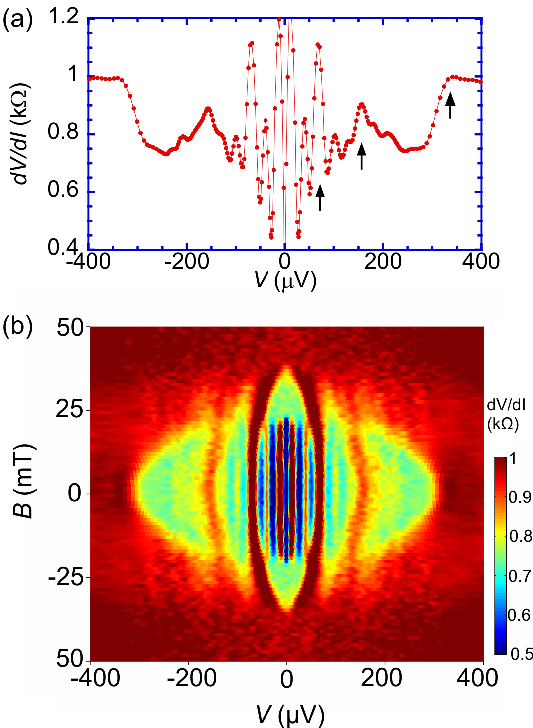
We have also measured the dependence of positions of the resistance features as a function of magnetic field. The differential resistance of device as function of magnetic field is shown in Fig. 11. In this device, the three MAR features are present (marked by arrows), which move smoothly towards lower voltages following the magnetic field dependence of the gap .
Besides the MAR features, the IVC of all the measured devices exhibit a number of structures at lower voltages, whose positions are independent of both temperature and magnetic field, see Fig. 10 and Fig. 11. These structures are therefore not associated with MAR. However, they are related to the superconducting state in the electrodes since they do not persist above the critical temperature and critical magnetic field and even disappear somewhat earlier.
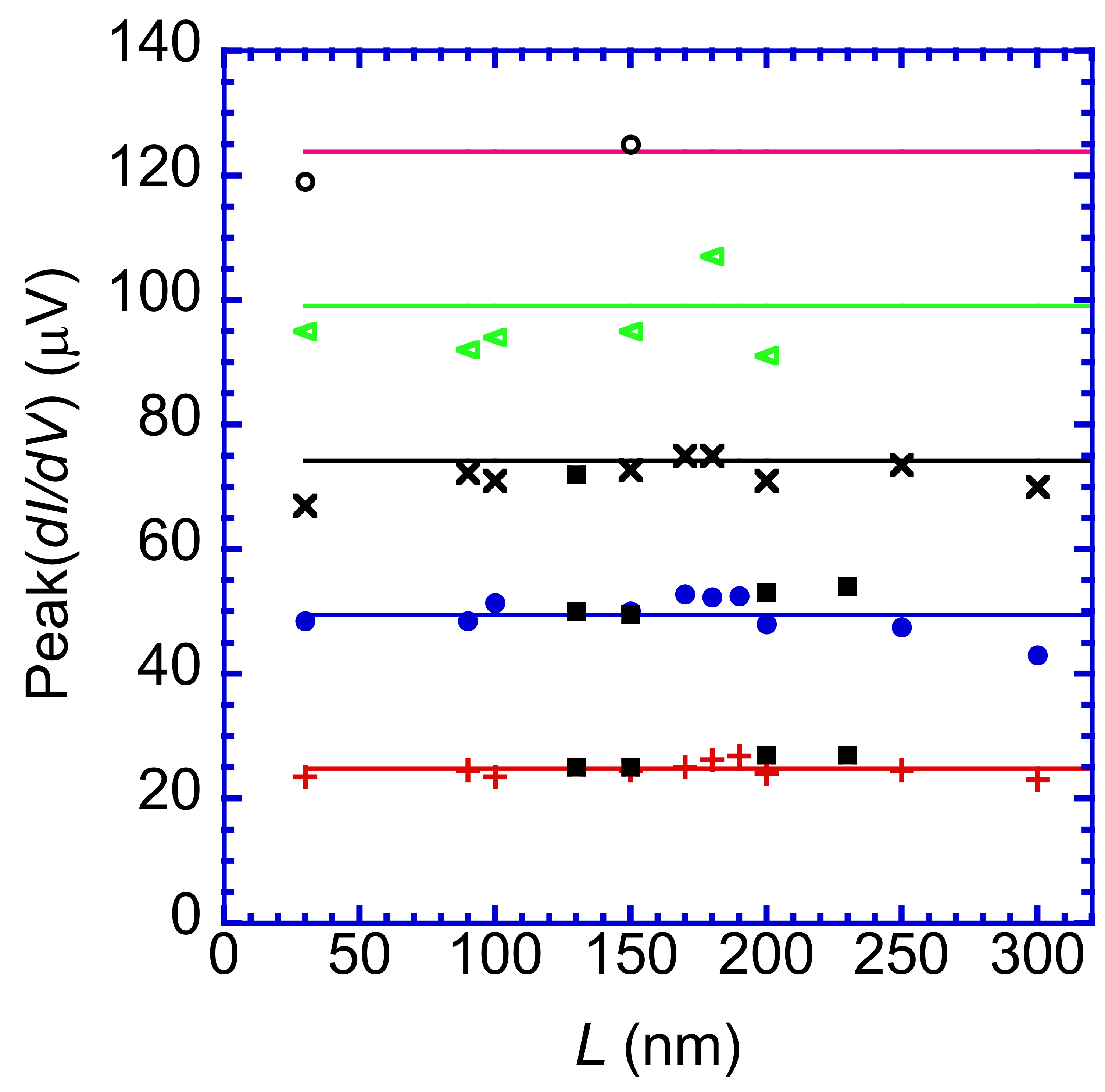
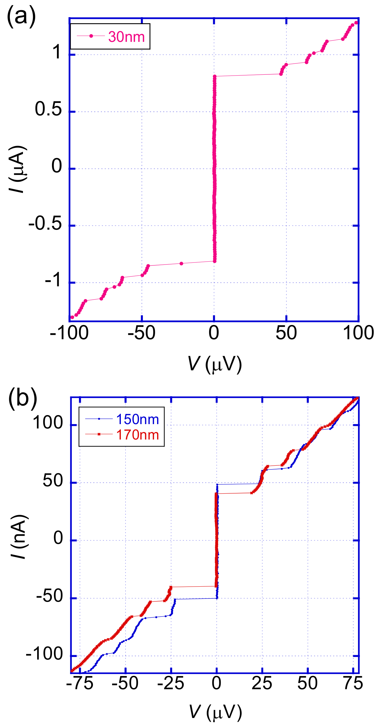
The origin of these structures is not clear. In Ref. Kretinin et al., similar structures were reported for suspended NW devices and attributed to resonances resulting from coupling of the ac Josephson current to mechanical vibrations in the wire. The fact that we observe such structures not only in suspended but also in non-suspended wires rules out this explanation. Furthermore, the phonon resonances would appear at voltages corresponding to the phonon eigen-frequencies, i.e. depend on the wire length (). We systematically measured the length dependence of the low-voltage, temperature independent structures, the results are presented in Fig. 12. The positions of the structures do not depend on the wire lengths neither for suspended nor non-suspended devices. The positions are given by the integer multiples of the same voltage, V.
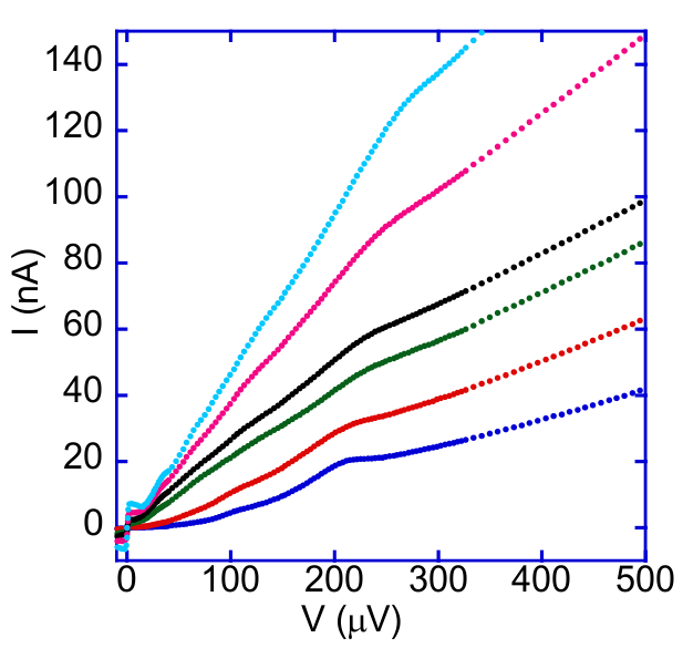
The fact that the positions of the temperature-independent structures are the same in different junctions makes it unlikely that they are related to external electromagnetic resonances, but rather result from some general intrinsic mechanism. To get a better insight in the origin of the temperature independent subgap structures we analyzed the shape of the IVC, see Fig. 13. In all investigated junctions the IVC have a staircase shape and consist of a number of successive voltage steps. Between the steps, the current continuously grows with the differential resistance increasing after every step. Such a behavior may be explained by successive emergence of normally conducting domains in the wire as soon as the current exceeds the critical value. This picture closely resembles the resistive states in superconducting whiskers containing phase slip centers (PSC).Meyer and Minnigerode (1972); Skocpol et al. (1974) Although one cannot in a straightforward way extend the PSC scenario in truly superconducting whiskersGalaiko and Kopnin (1986) to the proximity induced superconductivity in nanowires, one cannot exclude the possibility of formation of some kind of spatially inhomogeneous resistive state in the proximity region.
VIII Gate dependence
In this section, we investigate the gate dependence of the IVC in the superconducting state of suspended devices of type C shown in Fig. 1c and in Table I. The data presented in the in the previous sections are obtained at the zero gate voltage for the conduction regime with multiple open conducting channels. Here we discuss the change of the IVCs in this regime with variation of the gate voltage. An opposite, few-channel transport regime at large negative gate voltage, showing quantization of the normal conductance and the Josephson critical current was investigated in Ref. Abay et al., 2012.
In our device, the gate voltage controls the local carrier concentration in the nanowire and thereby affects the strength of the proximity effect. Due to a strong capacitive coupling of the gate to the wire, this variation is significant allowing us to observe a cross over from the SNS to SIS type regime of the current transport at low temperature. According to the theory,Bratus’ et al. (1995); Ingerman et al. (2001) the IVC of the transparent wire should exhibit, besides a large Josephson current, a large excess current both in the subgap voltage region and at the large voltage. On the other hand, more resistive wires should exhibit a small Josephson current, a suppressed subgap current, and a cross over to deficit (negative excess) current at large voltage.
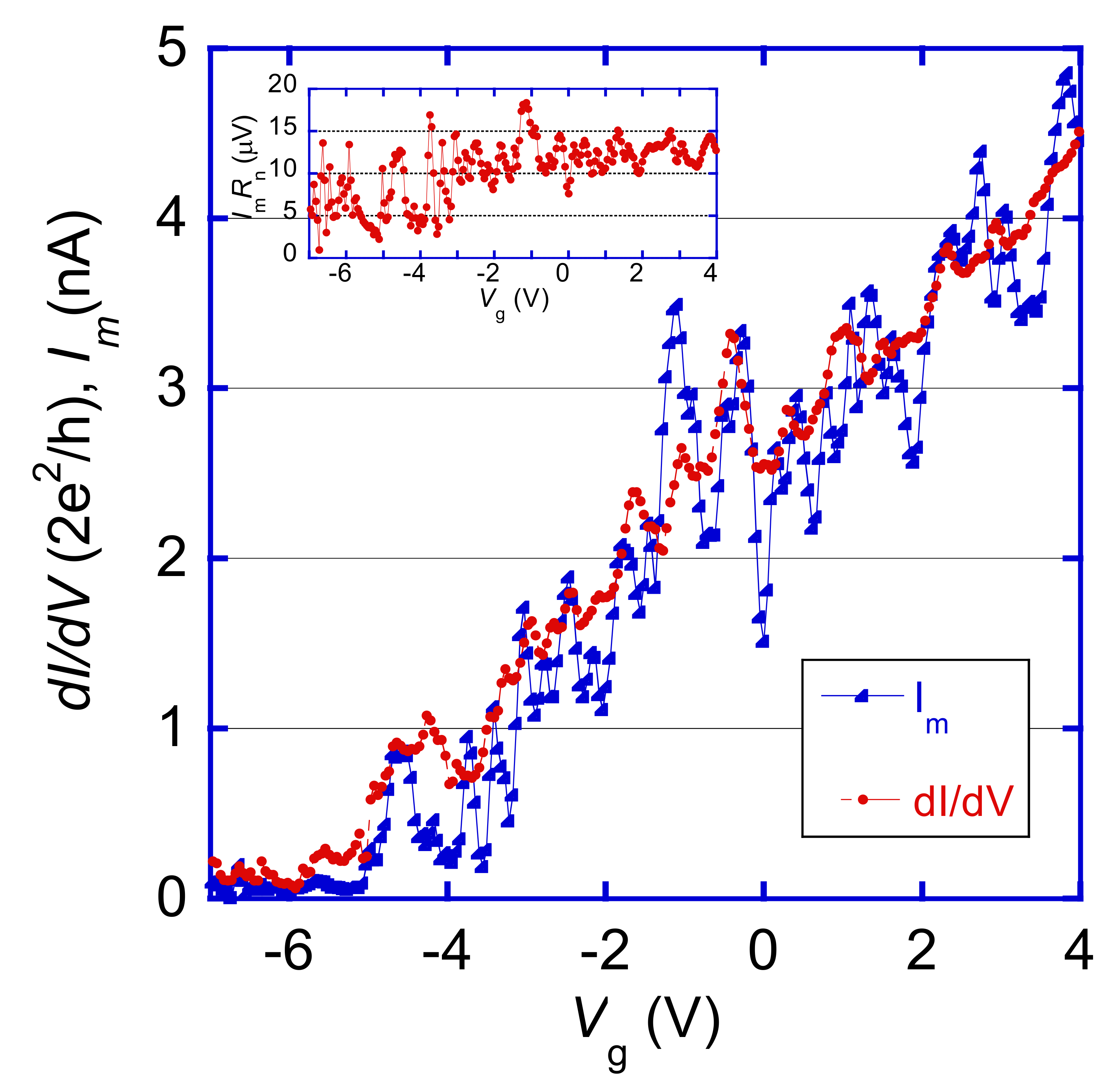
The dependence of the maximum Josephson current on the gate voltage is shown in Fig. 14 for the suspended device (nm). The change of the maximum current (blue) varies in tact with the change of the differential conductance (red). Owing to the n-type nature of the nanowires, the conductance and the maximum Josephson current are strongly suppressed at large negative gate voltages, V. Changing the gate voltage towards positive values results in linear increase of the averaged conductance and maximum Josephson current, the latter reaching the value of nA at V. Simultaneously, the product saturates at the value, V, and remains constant over a wide range of gate voltages, as shown in the inset in Fig. 14.
In Fig. 15 we present a set of IVCs for the suspended device C12 ( 200 nm and k) for gate voltages ranging from V to V. At large positive gate voltage, i.e. at large conductance, the IVC shows significant excess current and enhanced subgap conductance, indicating highly transmissive SNS regime. In the opposite limit of large negative gate voltage (small conductance), the IVC has a typical form for SIS tunnel junctions with negative excess currentBezuglyi et al. (2011) and strongly suppressed subgap conductance. The suppression of the subgap conductance is explained by small probability of MAR processes at small voltage, which scales with , where is the number of Andreev reflections. In the tunneling regime with small the subgap conductance is exponentially small. At the intermediate gate voltages the device exhibits continuous crossover between these two regimes in accordance with the theoretical predictions for contacts with varying transparency.Bratus’ et al. (1995); Ingerman et al. (2001)
IX Conclusion
We have investigated, both experimentally and theoretically, proximity effect in InAs nanowires connected to superconducting electrodes. We have fabricated and investigated a large number of nanowire devices with suspended gate controlled nanowires and non-suspended nanowires, with a broad range of lengths and normal state resistances. We measured current-voltage characteristics and analyzed their main features: the Josephson current, excess current, and subgap current as functions of length, temperature, magnetic field and gate voltage, and compared them with theory. The devices show reproducible resistance per unit length, and highly transmissive interfaces. The measured superconducting characteristics are consistent and agree reasonably well in most cases with theoretically computed values. The maximum Josephson current for a short length device, nm, exhibits a record high magnitude of nA at low temperature that comes close to the theoretically expected value. The maximum Josephson current in other devices is typically reduced compared to the theoretical values. The measured excess current in most of the devices is consistent with the normal resistance data and agrees well with the theory. The subgap current shows large number of structures, some of them are identified as subharmonic gap structures generated by MAR. The other structures, detected in both suspended and non-suspended devices, have the form of the voltage steps at voltages that are independent of either the superconducting gap or the length of the wire. By varying the gate voltage in suspended devices we were able to observe a cross over from typical tunneling transport, with suppressed subgap current and negative excess current, at large negative gate voltage to pronounced SNS-type behavior, with enhanced subgap conductance and large positive excess current, at large positive gate voltage.
Acknowledgements.
We acknowledge fruitful discussions with Lars Samuelson, Christopher Wilson, Thilo Bauch, and Jonas Bylander. The work was supported by the Swedish Research council, the Wallenberg foundation. HQX also acknowledges the National Basic Research Program of the Ministry of Science and Technology of China (Nos. 2012CB932703 and 2012CB932700).References
- Samuelson (2003) L. Samuelson, Mater. Today 6, 22 (2003).
- Thelander et al. (2006) C. Thelander, P. Agarwal, S. Brongersma, J. Eymery, L. Feiner, A. Forchel, M. Scheffler, W. Riess, B. Ohlsson, U. Gösele, and L. Samuelson, Mater. Today 9, 28 (2006).
- Li et al. (2006) Y. Li, F. Qian, J. Xiang, and C. M. Lieber, Mater. Today 9, 18 (2006).
- Dayeh (2010) S. A. Dayeh, Semicond. Sci. and Technol. 25, 024004 (2010).
- van Weperen et al. (2013) I. van Weperen, S. R. Plissard, E. P. A. M. Bakkers, S. M. Frolov, and L. P. Kouwenhoven, Nano Lett. 13, 387 (2013).
- Abay et al. (2013) S. Abay, D. Persson, H. Nilsson, H. Q. Xu, M. Fogelström, V. Shumeiko, and P. Delsing, Nano Lett. 13, 3614 (2013).
- Jespersen et al. (2009) T. S. Jespersen, M. L. Polianski, C. B. Sørensen, K. Flensberg, and J. Nygård, New J.Phys. 11, 113025 (2009).
- Xiang et al. (2006) J. Xiang, A. Vidan, M. Tinkham, R. M. Westervelt, and M. Lieber, Charles, Nat. Nanotechnol. 1, 208 (2006).
- Doh et al. (2005) Y.-J. Doh, J. A. van Dam, A. L. Roest, E. P. A. M. Bakkers, L. P. Kouwenhoven, and S. De Franceschi, Science 309, 272 (2005).
- Nilsson et al. (2012) H. A. Nilsson, P. Samuelsson, P. Caroff, and H. Q. Xu, Nano Lett. 12, 228 (2012).
- Abay et al. (2012) S. Abay, H. Nilsson, F. Wu, H. Xu, C. Wilson, and P. Delsing, Nano Lett. 12, 5622 (2012).
- Nishio et al. (2011) T. Nishio, T. Kozakai, S. Amaha, M. Larsson, H. A. Nilsson, H. Q. Xu, G. Zhang, K. Tateno, H. Takayanagi, and K. Ishibashi, Nanotechnology 22, 445701 (2011).
- Doh et al. (2008) Y.-J. Doh, S. D. Franceschi, E. P. A. M. Bakkers, and L. P. Kouwenhoven, Nano Lett. 8, 4098 (2008).
- Hofstetter et al. (2009) L. Hofstetter, S. Csonka, J. Nygård, and C. Schönenberger, Nature 461, 960 (2009).
- Mourik et al. (2012) V. Mourik, K. Zuo, S. M. Frolov, S. R. Plissard, E. P. A. M. Bakkers, and L. P. Kouwenhoven, Science 336, 1003 (2012).
- Deng et al. (2012) M. T. Deng, C. L. Yu, G. Y. Huang, M. Larsson, P. Caroff, and H. Q. Xu, Nano Lett. 12, 6414 (2012).
- Das et al. (2012) A. Das, Y. Ronen, Y. Most, Y. Oreg, M. Heiblum, and H. Shtrikman, Nature Phys. 8, 887 (2012).
- Kulik and Omel’yanchuk (1975) I. Kulik and A. Omel’yanchuk, Sov. Phys.–JETP Letters 21, 96 (1975).
- Klapwijk et al. (1982) T. Klapwijk, G. Blonder, and M. Tinkham, Physica B+C 109, 1657 (1982).
- (20) A. Kretinin, A. Das, and H. Shtrikman, arXiv:1303.1410 .
- Meyer and Minnigerode (1972) J. Meyer and G. Minnigerode, Phys. Lett. A 38, 529 (1972).
- Skocpol et al. (1974) W. Skocpol, M. Beasley, and M. Tinkham, J. Low Temp. Phys. 16, 145 (1974).
- Ohlsson (2002) B. Ohlsson, Physica E 13, 1126 (2002).
- Nilsson et al. (2008) H. A. Nilsson, T. Duty, S. Abay, C. Wilson, J. B. Wagner, C. Thelander, P. Delsing, and L. Samuelson, Nano Lett. 8, 872 (2008).
- Suyatin et al. (2007) D. B. Suyatin, C. Thelander, M. T. Björk, I. Maximov, and L. Samuelson, Nanotechnology 18, 105307 (2007).
- Datta (1997) S. Datta, Electronic Transport in Mesoscopic Systems (Cambridge University Press, 1997).
- Samuelsson et al. (2004) P. Samuelsson, A. Ingerman, G. Johansson, E. V. Bezuglyi, V. S. Shumeiko, G. Wendin, R. Kürsten, A. Richter, T. Matsuyama, and U. Merkt, Phys. Rev. B 70, 212505 (2004).
- Furusaki et al. (1992) A. Furusaki, H. Takayanagi, and M. Tsukada, Phys. Rev. B 45, 10563 (1992).
- Arnold (1987) G. Arnold, J. Low Temp. Phys. 68, 1 (1987).
- Bratus’ et al. (1995) E. N. Bratus’, V. S. Shumeiko, and G. Wendin, Phys. Rev. Lett. 74, 2110 (1995).
- Averin and Bardas (1995) D. Averin and A. Bardas, Phys. Rev. Lett. 75, 1831 (1995).
- Cuevas et al. (1996) J. C. Cuevas, A. Martín-Rodero, and A. L. Yeyati, Phys. Rev. B 54, 7366 (1996).
- (33) Cross over from diffusive short- to long-junction regime could alternatively be modeled with a theory developed in Ref. Bezuglyi et al., 2011.
- Cuevas and Fogelström (2001) J. C. Cuevas and M. Fogelström, Phys. Rev. B 64, 104502 (2001).
- Eschrig (2009) M. Eschrig, Phys. Rev. B 80, 134511 (2009).
- Zaitsev (1984) A. V. Zaitsev, Sov. Phys. –JETP 59, 1015 (1984).
- Shumeiko et al. (1997) V. S. Shumeiko, E. N. Bratus, and G. Wendin, Low Temp. Phys. 23, 181 (1997).
- Cuevas et al. (2006) J. C. Cuevas, J. Hammer, J. Kopu, J. K. Viljas, and M. Eschrig, Phys. Rev. B 73, 184505 (2006).
- Bezuglyi et al. (2011) E. V. Bezuglyi, E. N. Bratus’, and V. S. Shumeiko, Phys. Rev. B 83, 184517 (2011).
- Martinis and Grabert (1988) J. M. Martinis and H. Grabert, Phys. Rev. B 38, 2371 (1988).
- Ambegaokar and Halperin (1969) V. Ambegaokar and B. I. Halperin, Phys. Rev. Lett. 22, 1364 (1969).
- Bladh et al. (2003) K. Bladh, D. Gunnarsson, E. Hürfeld, S. Devi, C. Kristoffersson, B. Smålander, S. Pehrson, T. Claeson, P. Delsing, and M. Taslakov, Review of Scientific Instruments 74, 1323 (2003).
- Kupriyanov et al. (1999) M. Y. Kupriyanov, A. Brinkman, A. A. Golubov, M. Siegel, and H. Rogalla, Physica C 326, 16 (1999).
- Blonder et al. (1982) G. E. Blonder, M. Tinkham, and T. M. Klapwijk, Phys. Rev. B 25, 4515 (1982).
- Galaiko and Kopnin (1986) V. Galaiko and N. Kopnin, in Nonequilibrium Superconductivity, edited by D. Langenberg and A. Larkin (North-Holland, Amsterdam, 1986).
- Ingerman et al. (2001) A. Ingerman, G. Johansson, V. S. Shumeiko, and G. Wendin, Phys. Rev. B 64, 144504 (2001).