Electronic properties of Mn decorated silicene on hexagonal boron nitride
Abstract
We study silicene on hexagonal boron nitride, using first principles calculations. Since hexagonal boron nitride is semiconducting, the interaction with silicene is weaker than for metallic substrates. It therefore is possible to open a 50 meV band gap in the silicene. We further address the effect of Mn decoration by determining the onsite Hubbard interaction parameter, which turns out to differ significantly for decoration at the top and hollow sites. The induced magnetism in the system is analyzed in detail.
Silicon based nanostructures, such as two-dimensional silicene (an analogue to graphene) and silicene nanoribbons are currently attracting the interest of many researchers due to materials properties that are similar to but richer than those of graphene verri ; olle . Moreover, they are advantageous to carbon based nanostructures, as they can be expected to be compatible with the existing semiconductor industry. It is observed that the electronic band structure of silicene shows a linear dispersion around the Dirac point, like graphene, and hence is a candidate for applications in nanotechnology. Due to an enhanced spin orbit coupling a band gap 1.55 meV is opened yao . A mixture of and -type bonding results in a buckled structure, which leads to an electrically tunable band gap falko ; Ni . First-principles geometry optimization and phonon calculations as well as temperature dependent molecular dynamics simulations predict a stable low-buckled structure ciraci . Moreover, stability of silicene under biaxial tensile strain has been predicted up to 17% strain kaloni-jap .
Silicene and its derivatives experimentally have been grown on Ag and ZrB2 substrates padova ; vogt ; ozaki , though there is still discussion about the quality of the results Lin . On a ZrB2 thin film an asymmetric buckling due to the interaction with the substrate is found, which opens a band gap. In general, transition metal decorated graphene has been studied extensively both in experiment and theory. It has been predicted that 5 transition metal atoms show unique properties with topological transport effects. The large spin orbit coupling of 5 transition metal atoms together with substantial magnetic moments leads to a quantum anomalous Hall effect blugel . A model study also has predicted the quantum anomalous Hall effect for transition metal decorated silicene nanoribbons ezawa . Energy arguments indicate that transition metal atoms bond to silicene much stronger than to graphene. As a result, a layer by layer growth of transition metals could be possible on silicene Ni1
The deposition of isolated transition metal atoms on layers of hexagonal boron nitride on a Rh(111) substrate has been studied in Ref. fabian . The authors have demonstrated a reversible switching between two states with controlled pinning and unpinning of the hexagonal boron nitride from the metal substrate. In the first state the interaction of the hexagonal boron nitride is reduced, which leads to a highly symmetric ring in scanning tunneling microscopy images, while the second state is imaged as a conventional adatom and corresponds to normal interaction. Motivated by this work, we present in the following a first-principles study of the transition metal decoration of silicene on hexagonal boron nitride. We will first address the interaction with the substrate and then will deal with the electronic and magnetic properties of the Mn decorated system,
All calculations have been carried out using density functional theory in the generalized gradient approximation. We employ the Quantum-ESPRESSO package paolo , taking into account the van-der-Waals interaction grime . The calculations are performed with a plane wave cutoff energy of 816 eV, where a Monkhorst-Pack k-mesh is used to optimize the crystal structure and to obtain the self-consistent electronic structure. The atomic positions are relaxed until an energy convergence of 10-7 eV and a force convergence of 0.001 eV/Å are reached. To study the interaction of the silicene with the substrate, we employ a supercell consisting of a supercell of silicene on top of a supercell of hexagonal boron nitride. We have tested the convergence of the results with respect to the thickness of the substrate by taking into account 2, 3, 4, and 6 atomic layers of -BN, finding only minor differences (in particular concerning the splitting and position of the Dirac cone) because of the inert nature of the substrate. A thin substrate consequently turns out to be fully sufficient in the calculations. Moreover, the supercell of silicene fits well on the supercell of the substrate with a lattice mismatch of only 2.8%. When we consider Mn decorated silicene we use a larger supercell that contains 16 Si in a layer over 18 B and 18 N. While the onsite Hubbard parameter for 3 transition metal atoms is known to be several eV, we explicitly calculate the value in the present study for the different adsorption sites in order to obtain accurate results for the electronic and magnetic properties of the Mn decorated system.
In general, the lattice mismatch of 2.8% between silicene and hexagonal boron nitride can be expected to be small enough to avoid experimental problems with a controlled growth. Moreover, accurate measurements of materials properties can be difficult to achieve on metallic substrates, whereas the interaction is reduced on semiconducting substrates. Our calculated binding energy for the interface between silicene and hexagonal boron nitride is only 100 meV per Si atom, as compared to typically 500 meV per Si atom for an interface to a metallic substrate. Experimental realizations of graphene based electronic devices using hexagonal boron nitride as substrate on a Si wafer support are subject to various limitations, such as a poor on/off ratio kim . However, on this substrate graphene exhibits the highest mobility dean and a sizable band gap Gweon ; Ruge ; jmc . Since silicene resembles the structure of graphene, synthesis on hexagonal boron nitride thus has great potential.
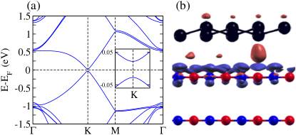
The structural arrangement of the system under study is depicted in Fig. 1(b), together with the charge redistribution introduced by the interaction with the substrate. We obtain SiSi bond lengths of 2.24 Å to 2.26 Å and a buckling of 0.48Å to 0.54 Å, which is slightly higher than in free-standing silicene yao ; ciraci . For the angle between the SiSi bonds and the normal of the silicene sheet we observe values of 113∘ to 115∘, again close to the findings for free-standing silicene (116∘). The optimized distance between the silicene and hexagonal boron nitride sheets forming the interface turns out to be 3.57 Å, which is similar to the distance at the contact between graphene and hexagonal boron nitride. In addition, the interlayer distance within the hexagonal boron nitride amounts to be 3.40 Å, whereas in a bilayer configuration values of 3.30 Å to 3.33 Å have been reported Marini ; shi .
The interaction between silicene and hexagonal boron nitride recently has been addressed by Liu and coworkers Zhao , who have reported a perturbation of the Dirac cone with an energy gap of 4 meV. This study has taken into account only a single layer of hexagonal boron nitride as substrate, so that a more realistic description may yield a different result. Indeed, we observe a perturbed Dirac cone with an energy gap of 50 meV in the band structure shown in Fig. 1(a). The and bands forming the Dirac cone are due to the orbitals of the Si atoms, while the bands related to the B and N atoms are located about 0.5 eV above and 1 eV below the Fermi energy. We find a small but finite charge redistribution across the interface to the substrate; see the charge density difference isosurfaces plotted in Fig. 1(b). As a result the Dirac cone is perturbed and the 50 meV energy gap is realized, which can be interesting for nanoelectronic device applications, in particular because an external electric field can be used to tune the gap. The isosurface plot also demonstrates that the Si atom closest to a B atom is subject to the strongest charge transfer, while for all other Si atoms charge transfer effects are subordinate due to longer interatomic distances.
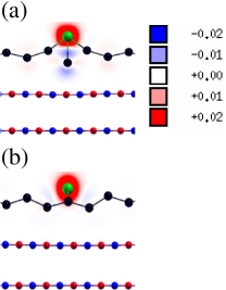
The possible decoration sites for a Mn atom on silicene can be classified as top, bridge, and hollow. Decoration at the bridge site is not considered in the following because the Mn atom immediately transfers to the top site. A side view of the relaxed structure for Mn decoration at the top site is given in Fig. 2(a), together with a spin density map. We obtain the onsite interaction parameter using a constraint-GGA method epl , and calculate the values of 3.8 eV for the Mn atom at the top site and 4.5 eV for the Mn atom at the hollow site. For the top site configuration, structural optimization reveals that the Mn atom moves close to an original Si position and thereby strongly displaces this Si atom, resulting in a short MnSi bond length of 2.43 Å. Moreover, the Mn atom is bound to three Si atoms with equal bond lengths of 2.45 Å. SiSi bond lengths of 2.24 Å to 2.28 Å are observed, which corresponds to a slight modification as compared to the pristine configuration. The buckling of the silicene, on the other hand, is strongly altered, now amounting to 0.45 Å to 0.67 Å. Accordingly, angles of 113∘ to 117∘ are found between the SiSi bonds and the normal of the silicene sheet. The height of the Mn atom above the silicene sheet is 1.30 Å. Finally, we note that the separation between the atomic layers of the hexagonal boron nitride is virtually not modified by the Mn decoration.
A side view of the relaxed structure for Mn decoration on the hollow site is shown in Fig. 2(b). In this case, the Mn atom does not displace a specific Si atom but stays close to the center of the Si hexagon. It is bound equally to the neighboring Si atoms with bond lengths of 2.40 Å to the upper three and 2.77 Å to the lower three Si atoms. A buckling of 0.46 Å to 0.62 Å, SiSi bond lengths of 2.23 Å to 2.28 Å, and angles to the normal of 112∘-117∘ are obtained. The Mn atom is located 1.01 Å above the silicene sheet and the separation between the atomic layers in the hexagonal boron nitride is slightly increased to 3.44 Å. In contrast, the distance between silicene and substrate here amounts to 3.55 Å and thus is significantly larger than in the case of decoration at the top site, because in the latter case one Si atom is displaced from the silicene sheet, which modifies the distance to the substrate. The calculated total energies indicate that decoration at the hollow site is by 33 meV favorable as compared to decoration at the top site.
We find total magnetic moments of 4.56 and 3.50 per supercell for Mn decoration at the top and hollow sites, a reduction of spin from the free Mn value of 5.0 unpaired electrons. The magnetization reduction is notable on the hollow site, which can be seen from Fig. 2 and 3 to involve greater immersion in and hybridization with the Si than the top site. By far the largest contribution to the magnetic moment comes from the Mn atom and only small moments are induced on the Si atoms. This can be clearly seen in the spin density maps presented in Figs. 3(a) and (b). For Mn decoration at the top site we obtain a Mn moment of 4.40 and a total of 0.16 from all the Si atoms, whereas for decoration at the hollow site the Mn moment amounts to 4.16 and the Si atoms contribute a total . These results indicate that the Mn and Si moments are ordered ferromagnetically and antiferromagnetically for decoration at the top and hollow sites, respectively.
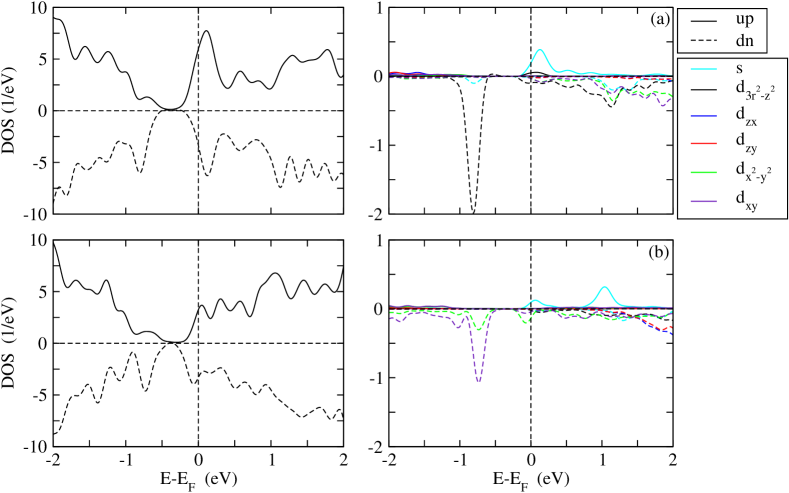
In Fig. 3 we address the density of states (DOS) for decoration at the (a) top and (b) hollow sites. The left panel of the figure shows the total DOS and the right panel the partial DOSs of the Mn and orbitals. In contrast to pristine silicene (band gap of 1.55 meV yao ), the DOSs show a region without states around 0.5 eV below the Fermi energy. This observation corresponds to an -doping due to the mentioned charge transfer from Mn to silicene. Closer inspection of the partial DOSs for decoration at the top site shows that the spin majority and as well as the spin minority , , and states contribute in the vicinity of the Fermi energy, while there are essentially no contributions from the and states. A sharp Mn peak is obsvered about 0.8 eV, which is due to the spin minority states. For decoration at the hollow site almost exclusively the spin majority and spin minority and states contribute around the Fermi energy. Two less pronounced DOS peaks appear 0.75 eV below the Fermi energy, contributed by the spin minority and states.
In conclusion, we have employed density functional theory to discuss the structure and chemical bonding of silicene on hexagonal boron nitride. The interaction results in a band gap of 50 meV. Furthermore, we have calculated the onsite Hubbard interaction parameter for Mn decoration at the top and hollow sites of the silicene, finding values of 3.8 eV and 4.5 eV, respectively. The electronic and magnetic properties of Mn decorated silicene have been studied in detail. In particular, magnetic moments of 3.50 and 4.56 , respectively, have been obtained for Mn decoration at the top and hollow sites. Interestingly, the orientation between the Mn and induced Si moments is ferromagnetic in the former and antiferromagnetic in the latter case.
References
- (1) G. G. Guzmán-Verri and L. C. L. Y. Voon, Phys. Rev. B 76, 075131 (2007).
- (2) S. Lebegue and O. Eriksson, Phys. Rev. B 79, 115409 (2009).
- (3) C.-C. Liu, W. Feng, and Y. Yao, Phys. Rev. Lett. 107, 076802 (2011).
- (4) N. D. Drummond, V. Zólyomi, and V. I. Fal′ko, Phys. Rev B 85, 075423 (2012).
- (5) Z. Ni, Q. Liu, K. Tang, J. Zheng, J. Zhou, R. Qin, Z. Gao, D. Yu, and J. Lu, Nano Lett. 12, 113 (2012).
- (6) S. Cahangirov, M. Topsakal, E. Aktürk, H. Sahin, and S. Ciraci, Phys. Rev. Lett. 102, 236804 (2009).
- (7) T. P. Kaloni, Y. C. Cheng, and U. Schwingenschlögl, J. Appl. Phys. 113, 104305 (2013).
- (8) P. De Padova, C. Quaresima, C. Ottaviani, P. M. Sheverdyaeva, P. Moras, C. Carbone, D. Topwal, B. Olivieri, A. Kara, H. Oughaddou, B. Aufray, and G. Le Lay, Appl. Phys. Lett. 96, 261905 (2010).
- (9) P. Vogt, P. De, C. Quaresima, J. Avila, E. Frantzeskakis, M. C. Asensio, A. Resta, B. Ealet, and G. Le Lay, Phys. Rev. Lett. 108, 155501 (2012).
- (10) A. Fleurence, R. Friedlein, T. Ozaki, H. Kawai, Y. Wang, and Y. Yamada-Takamura, Phys. Rev. Lett. 108, 245501 (2012).
- (11) C.-L. Lin, R. Arafune, K. Kawahara, M. Kanno, N. Tsukahara, E. Minamitani, Y. Kim, M. Kawai, and N. Takagi, Phys. Rev. Lett. 110, 076801 (2013).
- (12) H. Zhang, C. Lazo, S. Blügel, S. Heinze, and Y. Mokrousov, Phys. Rev. Lett. 108, 056802 (2012).
- (13) M. Ezawa, Phys. Rev. Lett. 109, 055502 (2012).
- (14) X. Lin and J. Ni, Phys. Rev. B 86, 075440 (2012).
- (15) F. D. Natterer, F. Patthey, and H. Brune, Phys. Rev. Lett. 109, 066101 (2012).
- (16) P. Giannozzi, S. Baroni, N. Bonini, M. Calandra, R. Car, C. Cavazzoni, D. Ceresoli, G. L. Chiarotti, M. Cococcioni, I. Dabo, A. Dal Corso, S. de Gironcoli, S. Fabris, G. Fratesi, R. Gebauer, U. Gerstmann, C. Gougoussis, A. Kokalj, M. Lazzeri, L. Martin-Samos, N. Marzari, F. Mauri, R. Mazzarello, S. Paolini, A. Pasquarello, L. Paulatto, C. Sbraccia, S. Scandolo, G. Sclauzero, A. P. Seitsonen, A. Smogunov, P. Umari, and R. M. Wentzcovitch, J. Phys.: Condens. Matter 21, 395502 (2009).
- (17) S. Grimme, J. Comput. Chem. 27, 1787 (2006).
- (18) K. Kim, J.-Y. Choi, T. Kim, S.-H. Cho, and H.-J. Chung, Nature 479, 338 (2011).
- (19) C. R. Dean, A. F. Young, I. Meric, C. Lee, L. Wang, S. Sorgenfrei, K. Watanabe, T. Taniguchi, P. Kim, K. L. Shepard, and J. Hone, Nat. Nanotechnol. 5, 722 (2010).
- (20) S. Y. Zhou, G.-H. Gweon, A. V. Fedorov, P. N. First, W. A. de Heer, D.-H. Lee, F. Guinea, A. H. Castro Neto, and A. Lanzara, Nature Mater. 6, 770 (2007).
- (21) R. Quhe, J. Zheng, G. Luo, Q. Liu, R. Qin, J. Zhou, D. Yu, S. Nagase, W.-N. Mei, Z. Gao, and J. Lu, NPG Asia Materials 4, 1 (2012).
- (22) T. P. Kaloni, Y. C. Cheng, and U. Schwingenschlögl, J. Mater. Chem. 22, 919 (2012).
- (23) A. Marini, P. Garcia-Gonzalez, and A. Rubio, Phys. Rev. Lett. 96, 136404 (2006).
- (24) Y. Shi, C. Hamsen, X. Jia, K. K. Kim, A. Reina, M. Hofmann, A. L. Hsu, K. Zhang, H. Li, Z.-Y. Juang, M. S. Dresselhaus, L.-J. Li, and J. Kong, Nano Lett. 10, 4134 (2010).
- (25) H. Liu, J. Gao, and J. Zhao, J. Phys. Chem. C 117, 10353 (2013).
- (26) G. K. H. Madsen and P. Novák, EPL 69, 777 (2005).